Optical models
Light sources
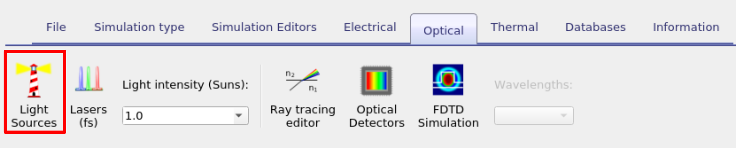
In OghmaNano light comes from light sources. Light sources defined in the light source editor this can be found in the Optical ribbon of the main window see figure 10.1.
The light source editor is shown below in Figure 10.3. Each light source consists of of illumination spectra and optical filters. In this way you can define a light source to emit AM1.5G but then filter out various components of the spectrum. This enables one to simulate for example a device under AM1.5G spectra but behind a thick glass contact that takes sunlight below 300 nm. Light sources can be combined in the Light source tab, so for example one could combine AM1.5G and light given off by a fluorescent tube. Each spectrum is multiplied by a multiplier defined in the multiplier column this defines the relative intensity of the light sources.
In the filters tab you can define the optical filters. They can be enabled or disabled using the Enable switch, you can select the material which will act as a filter, and decide how much the filter attenuates in dB.
The configure tab of each filter can be used to select where the light comes from, options are:
-
Top: Light will come form the top of the device. (y0) This is usually used with the transfer matrix solver. See the bottom left of figure 10.7.
-
Bottom: Light will come from the bottom of the device. (y1) This is usually used with the transfer matrix solver. See the bottom right of figure 10.7.
-
xyz: The light can come from an xyz position in the simulation space this used for FDTD simulations or ray tracing simulations. This can be seen in to bottom right of figure 10.7.
Stop and start wavelengths can also be set in the configure tab.
Local ground view factor
The local ground view factor which is given as
\[F_{ground}=sin^2 \left ( \frac{\theta_t}{2}\right )=\frac{1-cos(\theta_t)}{2}\]
can be set in the configure tab.
 |
 |
 |
 |
 |
 |
Transfer matrix model
In general the transfer matrix method is good for simulating sandwich type structures where light is incident normal to the surface of a device. Examples of such devices are solar cells, optical filters or sensors. This method is good for understanding optical absorption, reflection and transition in these structures. There are other more complex methods which can accomplish the same task such as FDTD, however general speaking the transfer matrix model will be orders of magnitude faster than these methods.
The user interface
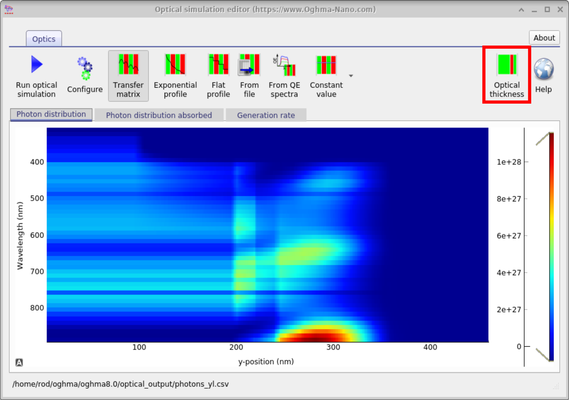
The transfer matrix simulation tool can be reached from the Optical ribbon in the main window by selecting Transfer matrix. If you click Run optical simulation (see 10.8) the distribution of light within the structure will be calculated as a function of position and wavelength. You can see from the top of the figure that there are various simulation modes. The full transfer matrix method is selected by selecting Transfer matrix, this will do full optical simulation. The other buttons represent other simplified approximations to the transfer matrix method that allow the user to explore more simple charge carrier generation profiles. From the left the push buttons in Figure 10.8 represent the following optical models:
-
Transfer matrix: This is a full transfer matrix simulation that takes into account multiple reflections from the interfaces and optical loss within the structure. This is in effect solving the wave equation in 1D and is an accurate (and recommended) optical model to use. See section 10.2.4. If you are unsure which model to pick, pick this one.
-
Exponential profile: This is a very simple optical model that assumes light decays exponentially according to the relation \[I=I_{0}e^{-\alpha x} \label{efield2}\] between layers and and assumes light is transmitted between layers according to the formula: \[T=1.0-\frac{n_1-n_0}{n_1+n_0} \label{equ:transfermatrixreflection}\] No reflection is accounted for.
-
Flat profile: The flat profile assumes light is constant within layers and only decreases at material interfaces according to equation [equ:transfermatrixreflection]. One might want to use this model when trying to understand the charge carrier dynamics in a device but wants to remove the effects of a non-uniform charge generation generation profile.
-
From file: This can be used to import generation profiles from a file. It us generally used to import the results of more complex optical simulations such as those from external FDTD solvers.
-
Constant value: If you click on the arrow to the right of the simulation button you will be able to set the charge carrier generation rate within each layer by hand. Again this is generally used when trying to understand charge carrier dynamics or device performance without to consider a complex optical profile. This would allow one to plot graphs of charge generation rate v.s. \(V_{oc}\) etc..

The optical simulation window has various tabs which can be used to explore how light interacts with the device. These can be seen in figure 10.12. The the top left image shows the photon density within the device, the image on the right shows the total photon density within the layers of the device. Notice how the reflection of the light of various layers causes interference patterns. The image on the bottom left shows the configuration of the optical model. A key parameter that can be seen in this window is the Photon efficiency, this parameter determines how many electron-hole pairs each photon that is absorbed within the active layer generates. In organic devices it accounts for geminate recombination, in other types of devices it should be set close to 1.0. Bottom right shows the same figure as in the top right of the figure, except by right clicking and playing with the menu options the figure has been converted into band diagram. This can be useful for generating band diagram figures for papers.
 |
 |
 |
 |
Running the transfer matrix simulation
As described above, the transfer matrix simulation can be run by directly clicking on the play button. However when running an electrical simulation the optical model is run automaticity without any user interaction. The only difference between the two ways of calling the optical simulation is that when the user directly calls the optical model more output files are written to disk, however when the optical simulation is run as part of an electrical simulation the number of files and output are limited as to not slow the electrical simulation.
Output files
After having run an optical simulation an overview of the results can be seen in the optical simulation window (Figure 10.8) as described above. However more in depth information can be obtained from the Output tab of the main window as shown in Figure 10.13.
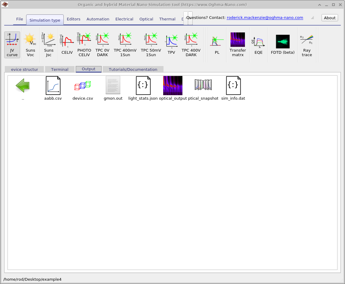
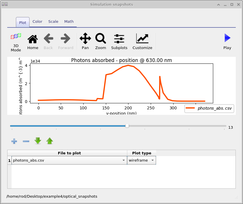
In Figure 10.13 you can see two icons one called Optical output and the other called optical_snapshots (in the figure it reads "ptica_output" due to the text being hidden). If you double click on Optical output it will bring up figure 10.8. If you double click on optical_snapshots it will bring up Figure 10.14. The optical snapshot window allows the user to view photon density, absorbed photons and electric field of the light. The information is displayed per wavelength so a detailed overview of device performance can be gained.
The optical_snapshots directory in depth
The optical_snapshots folder was described above and when accessed through the graphical interface allows the user to access photon density, absorbed photons and electric field of the light as a function of wavelength. However, it is simply a normal directory and the user can access it through a file explorer. If you open the directory using a tool such as windows explorer you will see something comparable to what is shown on the left of Figure 10.16. You can see folders numbered from 0 to 12 each folder represents a simulated wavelength. If you open a directory, say number 0, you will be presented with the files shown in the right hand of figure 10.16. These files contain the following information:
| File name | Description | |
|---|---|---|
| \(alpha.csv\) | y-position v.s. absorption @ given wavelength | |
| \(data.json\) | json file containing wavelength value | |
| \(En.csv\) | y-position (m) v.s. Electric field with -ve component (V/m) @ given wavelength | |
| \(Ep.csv\) | y-position (m) v.s. Electric field with +ve component (V/m) @ given wavelength | |
| \(G.csv\) | y-position (m) v.s. Generation rate (\(m^{-3} s^{-1}\)) | |
| \(n.csv\) | y-position (m) v.s. Real part of the refractive index n (au) @ given wavelength | |
| \(photons.csv\) | y-position (m) v.s. photon density (\(m^{-3}\)) @ given wavelength | |
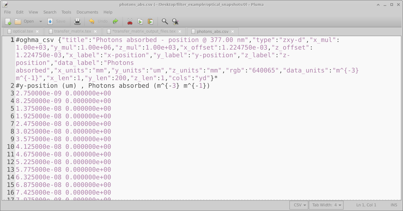
| \(photons\_abs.csv\) | y-position (m) v.s. photons absorbed (\(m^{-3} s^{-1}\)) @ given wavelength |
 |
 |
These files are simply plain text, if you open one it will look like 10.17. The first line of this file contains some information about the content of the file to help with plotting. The second line tells the user what the x and y axis contain then the following lines contain the data.
The optical_output folder in depth
While the optical_snapshots directory allows data to be plotted per simulated wavelength, the optical_output gives 2D maps of wavelength v.s. position for various simulation parameters. The content of the directory is shown in figure 10.18.
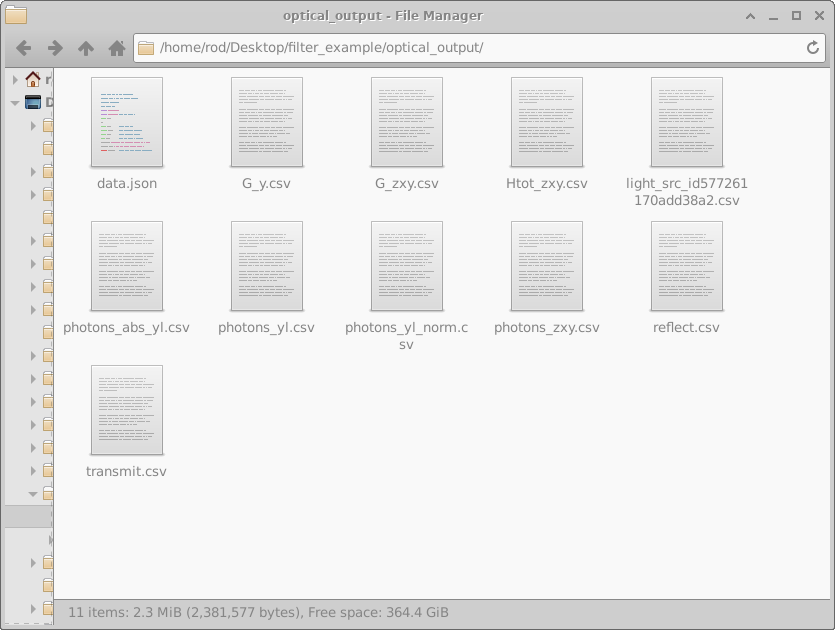
The files shown in Figure 10.18 are described in table 10.2.
| File name | Description | Plot type |
|---|---|---|
| data.json | Miscellaneous simulation information in json format | 1D |
| G_y.csv | y-position (m) v.s. Charge generation rate (\(m^{-3} s^{-1}\)) | 2D |
| G_zxy.csv | zxy-position (m) v.s. Charge generation rate (\(m^{-3} s^{-1}\)) | 2D |
| Htot_zxy.csv | zxy-position (m) v.s. Optical heat generation (\(W m^{-3}\)) | 2D |
| light_src_id_xxx.csv | wavelength (m) v.s. Light intensity from source (\(W/m\)) | 2D |
| photons_abs_yl.csv | wavelength (m) v.s. y-position (m) v.s. photons absorbed (\(m^{-3} s^{-1}\)) | 2D |
| photons_yl.csv | wavelength (m) v.s. y-position (m) v.s. Photon density (\(m^{-3} s^{-1}\)) | 2D |
| photons_yl_norm.csv | wavelength (m) v.s. y-position (m) v.s. Normalized photons (au) | 2D |
| reflect.csv | wavelength (m) v.s. Light reflected from the stack | 1D |
| transmit.csv | wavelength (m) v.s. Transmitted though the stack | 1D |
Simulating optically thick layers (incoherent layers)
Typical optoelectronic devices have layer thicknesses between 10 nm and 100 nm. However often these devices are deposited on top of substrates that are between 10 mm and 1 cm thick and often one wants to not only simulate the device but also the impact of the substrate. Thus to perform this type of simulation one will need a simulation tool that covers length scales from the nm top the meter scale. There are three problems with doing this:
-
Problem 1: Simulating different length scales: Computers don’t like doing maths with numbers that are very big and small very often this results in large computational/rounding errors, there is more on this in secton 9.11.1.1.
-
Problem 2: The wavelength of light: The wavelength of light is far smaller than 1 cm thus to get sensible answers out of the simulation one will need a very large number of mesh points correctly represent the constructive/negative interference of the light within the layer.
-
Problem 3: The light will not be coherent: The transfer matrix model assumes light comes from a single direction at 90 degrees to the interface and there are no defects in the material. For a thick layer this will not be true.
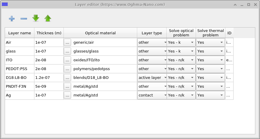
To get around these issues OghmaNano uses two strategies. The first is to give the user the option to only consider absorption and neglect phase changes within a layer, to form a so called incoherent layer (this solves problem 2 and 3). This can be selected from the layer editor in the main window see Figure 10.19. Notice in the column entitled Solve optical problem, the first two layers (air and glass) have Yes - k selected, and the other layers have Yes - n/k selected. This means that in layers with Yes - n/k phase changes of the light will be considered but in the layers marked Yes - k only attenuation losses will be accounted for and thus it can be thought of as an incoherent layer.
To get around the problem of having to simulate different length scales (problem 1) OghmaNano allows the user to set an effective optical depth for any layer. So one can for example setup a layer in the layer editor of width 100 nm, but set it’s effective depth to a much larger value such as 1 m. This works by multiplying the absorption coefficient of the layer by the ratio:
\[\alpha_{effective}(\lambda)=\alpha(\lambda) \frac{L_{effective}}{L_{simulation}} \label{effective_depth}\]
Where \(\alpha_{effective}\) is the effective absorption used in the simulation, \(\alpha\) is the true value of absorption for the material, \(L_{effective}\) is the effective layer thickness (say 1 m or 1 km), and \(L_{simulation}\) is the thickness of the layer in the simulation window. Not only does this approach reduce numerical issues (problem 1) but it also allows the user to plot meaningful graphs of the simulation results, without most of the plot taken up by the substrate and the device only appearing as a tiny slither on the edge of the graph.
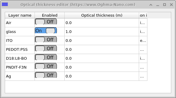
If you want to use this feature, then set up a device structure as shown in 10.19 then in the transfer matrix window click the Optical Thickness button (top right of Figure [fig:optical_thickness]). Then the window [fig:optical_thickness_window] will appear. In this window you can set the effective optical thickness of any layer. In this case we have set the glass to be 1 meter thick.
 [fig:optical_thickness]
 [fig:optical_thickness_window]
Theory of the transfer matrix method
On the left of the interface the electric field is given by
\[E_{1}=E^{+}_{1} e^{-j k_1 z}+E^{-}_{1} e^{j k_1 z} \label{efield1}\] and on the right hand side of the interface the electric field is given by \[E_{2}=E^{+}_{2} e^{-j k_2 z}+E^{-}_{2} e^{j k_2 z} \label{efield2}\]
Maxwel’s equations give us the relationship between the electric and magnetic fields for a plane wave.
\[\nabla \times E=-j\omega \mu H\] which simplifies to: \[\frac{\partial E} {\partial z}=-j\omega \mu H \label{maxwel}\]
Applying equation [maxwel] to equations [efield1]-[efield2], we can get the magnetic field on the left of the interface \[-j \mu \omega H^{y}_{1}=-j k_1 E^{+}_{1} e^{-j k_1 z}+j k_1 E^{-}_{1} e^{j k_1 z}\] and on the right of the interface \[-j \mu \omega H^{y}_{2}=-j k_2 E^{+}_{2} e^{-j k_2 z}+j k_2 E^{-}_{2} e^{j k_2 z}.\]
Tidying up gives, \[H^{y}_{1}=\frac{k}{\omega \mu}E^{+}_{1} e^{-j k_1 z}-\frac{k}{\omega \mu} E^{-}_{1} e^{j k_1 z}\]
\[H^{y}_{2}=\frac{k}{\omega \mu}E^{+}_{2} e^{-j k_2 z}-\frac{k}{\omega \mu} E^{-}_{2} e^{j k_2 z}\]
Boundary conditions
We now apply the electric and magnetic boundary conditions \[\mathbf{n} \times (\mathbf{E_2}-\mathbf{E_1})=0\]
\[\mathbf{n} \times (\mathbf{H_2}-\mathbf{H_1})=0\]
We let the interface be at z=0, which gives, \[(E_{2}^{+}+E_{2}^{-})-(E_{1}^{+}+E_{1}^{-})=0 \label{electric_boundary}\] and \[\frac{k_1}{\omega \mu}(E_{2}^{+}-E_{2}^{-})-(E_{1}^{+}-E_{1}^{-})\frac{k_2}{\omega \mu}=0\] . The wavevector is given by \[k=\frac{2 \omega }{\lambda}=\frac{\omega n}{c}\] . We can therefore write the magnetic boundary condition as \[n_2 (E_{2}^{+}-E_{2}^{-}) - n_1 (E_{1}^{+}-E_{1}^{-})=0 \label{mag_boundary}\]
Forward propagating wave
Rearrange equation, [mag_boundary] to give,
\[E_{1}^{-} = E_{1}^{+}-\frac{n_2}{n_1}(E_{2}^{+}-E_{2}^{-})\] Inserting in equation [electric_boundary], gives \[E_{2}^{+}+E_{2}^{-}=E_{1}^{+}+E_{1}^{+}-\frac{n_2}{n_1}(E_{2}^{+}-E_{2}^{-})\]
\[2E_{1}^{+}=E_{2}^{+}+E_{2}^{-}+\frac{n_2}{n_1}(E_{2}^{+}-E_{2}^{-})\]
\[2E_{1}^{+}\frac{n_1}{n_1+n_2}=E_{2}^{+}+E_{2}^{-}\frac{n_1-n_2}{n_1+n_2}\]
Backwards propagating wave
Rearrange equation, [mag_boundary] to give,
\[E_{1}^{+}=E_{1}^{-} +\frac{n_2}{n_1}(E_{2}^{+}-E_{2}^{-})\]
Inserting in equation [electric_boundary], gives \[E_{2}^{+}+E_{2}^{-}=E_{1}^{-} +\frac{n_2}{n_1}(E_{2}^{+}-E_{2}^{-})+E_{1}^{-}\]
\[2E_{1}^{-}=E_{2}^{+}+E_{2}^{-}- \frac{n_2}{n_1}(E_{2}^{+}-E_{2}^{-})\]
\[2E_{1}^{-}\frac{n_1}{n_1+n_2}=E_{2}^{+}\frac{n_1-n_2}{n_1+n_2}+E_{2}^{-}\] Which is the same result as obtained in .
These equations become:
\[E_{1}^{-}t_{12}=E_{2}^{+}r_{12}+E_{2}^{-}\]
and \[E_{1}^{+}t_{12}=E_{2}^{+}+E_{2}^{-}r_{12}\]
Accounting for propagation we can write. Note the change in sign between and this work, this is because of how I have defined my wave equation. \[E_{1}^{+}t_{12}=E_{2}^{+}e^{\zeta_2 d_1}+E_{2}^{-}r_{12}e^{-\zeta_2 d_1}\] and
\[E_{1}^{-}t_{12}=E_{2}^{+}r_{12}e^{\zeta_2 d_1}+E_{2}^{-}e^{-\zeta_2 d_1}\]
where \[\zeta=\frac{2\pi}{\lambda} \bar{n}\]
For a device with non reflecting back contacts:
\(\begin{pmatrix} e^{\zeta d} & 0 & 0 & 0 &r_{01}e^{-\zeta d} & 0 & 0 & 0 \\ -t_{12} & e^{\zeta d} & 0 & 0 &0 & r_{12}e^{-\zeta d} & 0 & 0 \\ 0 & -t_{23} & e^{\zeta d} & 0 &0 & 0 & r_{23}e^{-\zeta d} & 0 \\ 0 & 0 & -t_{34} & e^{\zeta d} & 0 & 0 & 0 & r_{34}e^{-\zeta d} \\ 0 &r_{12}e^{\zeta d_1} & 0 & 0 & -t_{12} &e^{-\zeta d} & 0 & 0 \\ 0 &0 & r_{23}e^{\zeta d} & 0 & 0 &-t_{23} & e^{-\zeta d} & 0 \\ 0 &0 & 0 & r_{34}e^{\zeta d} & 0 &0 & -t_{34} & e^{-\zeta d} \\ 0 &0 & 0 & 0 & 0 &0 & 0 & -t_{45} \\ \end{pmatrix} \begin{pmatrix} E_{1}^{+} \\ E_{2}^{+} \\ E_{3}^{+} \\ E_{4}^{+} \\ E_{1}^{-} \\ E_{2}^{-} \\ E_{3}^{-} \\ E_{4}^{-} \\ \end{pmatrix} = \begin{pmatrix} t_{01}E_{external} \\ 0 \\ 0 \\ 0 \\ 0 \\ 0 \end{pmatrix}\)
Refractive index and absorption
\[E(z,t)=Re(E_0 e^{j(-kz+\omega t)})= Re(E_0 e^{j(\frac{-2 \pi (n+j\kappa)}{\lambda}z + \omega t)})=e^{\frac{2\pi\kappa z}{\lambda}}Re(E_0 e^{\frac{j(-2 \pi (n+j\kappa)}{\lambda}z +\omega t})\] And because the intensity is proportional to the square of the electric field the absorption coefficient becomes
\[e^{-\alpha x}=e^{\frac{2\pi\kappa z}{\lambda}}\]
\[\alpha=-\frac{4\pi\kappa}{\lambda_0}\]
Optical mode solve 1D/2D
Related YouTube videos:
 |
Tutorial on calculating TE/TM modes in slab waveguides |
Text to be added later.
Finite Difference Time Domain
Finite Difference Time Domain (FDTD) is a very computationally intensive way to simulate the propagation of electromagnetic radiation. It solves full on Maxwell’s equations in time domain making no assumptions. This approach has only been possible in the last few years with the increase in computing power.
Food for thought: Before using FDTD, you should be aware that in many cases when simulating a device, using FDTD is like using a sledge hammer to crack a nut. For example when simulating a standard solar cell, one could use FDTD, this would involve simulating a wave front entering the cell through the top contact in time domain and waiting until the optical field reaches steady state then calculating how much light is being absorbed. This would require thousands of time domain simulation steps per wavelength. However usually one is not interested in the time evolution of light in a solar cell as sunlight varies very slowly indeed, so one is better off not using a steady state method but other methods which assume light has already reached steady state, such as the transfer matrix method discussed above.
Never the less, FDTD is an import method, and can be used to design and understand complex devices.
Related YouTube videos:
|
Generating photonic crystal structures for FDTD simulation |
|
Tutorial on simulating photonic crystal waveguides using FDTD |
Running an FDTD simulation
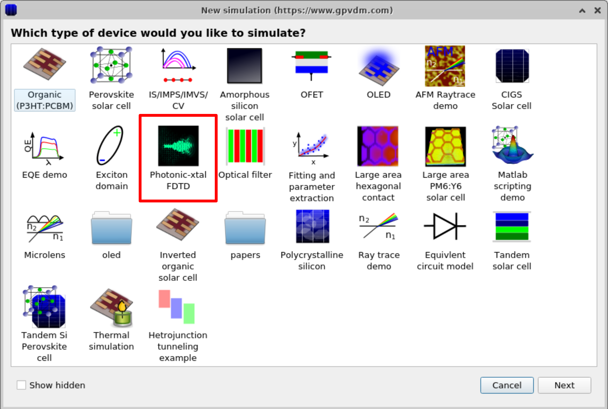
There is a demo FDTD simulation in the new simulations window. To open this click on new simulation in the file ribbon of the main window. The window in figure 10.20 will appear. Double click on the "Photonic-xtal FDTD" simulation to open it. Save the simulation on your local hard disk, don’t save it on a remote disk, USB disk or OneDrive they will be too slow to run the simulation.
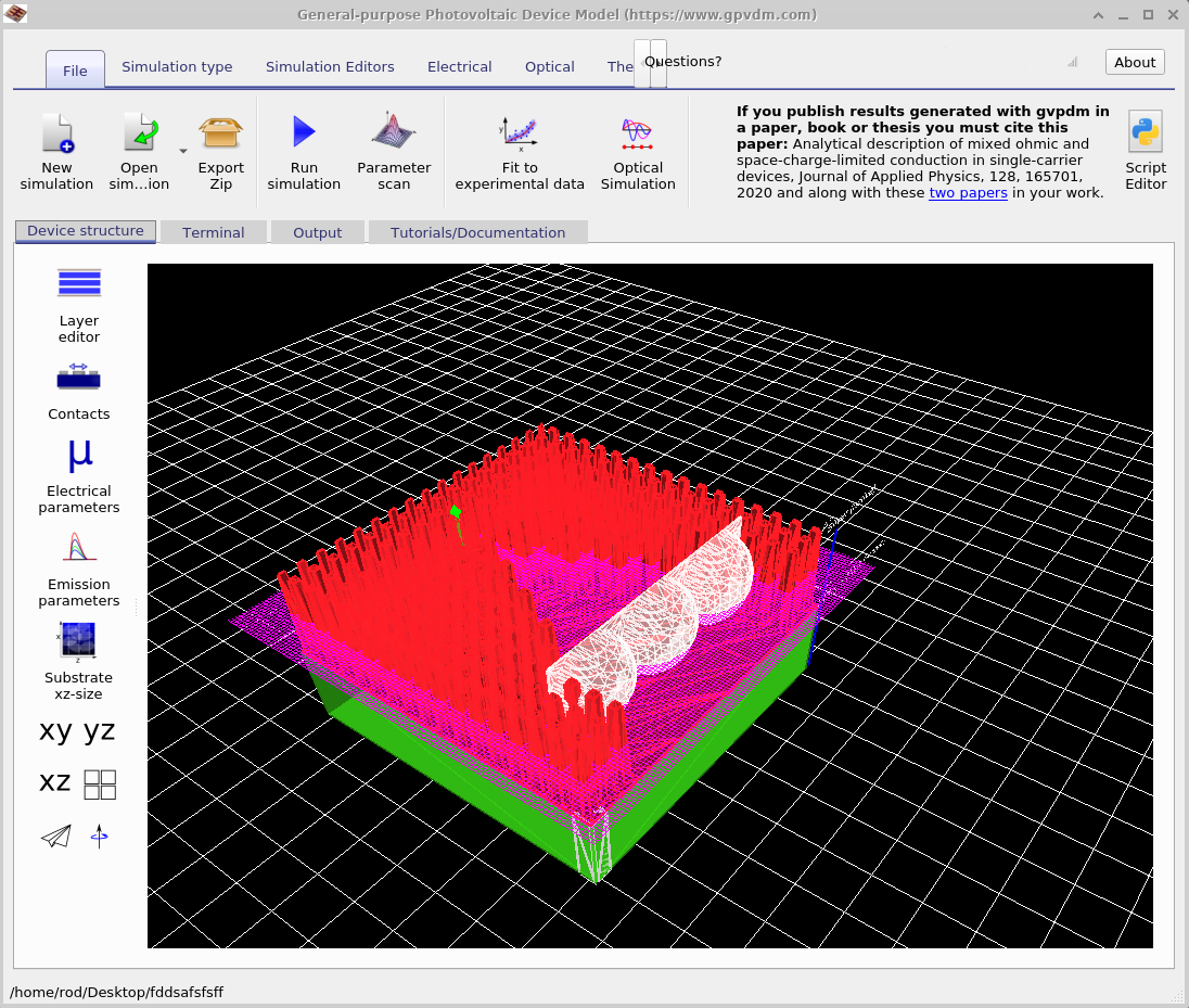
Once you have opened the simulation you should get a window which appears figure 10.21. If you click on the play button the FDTD simulation will run, it will take around 30 seconds to run.
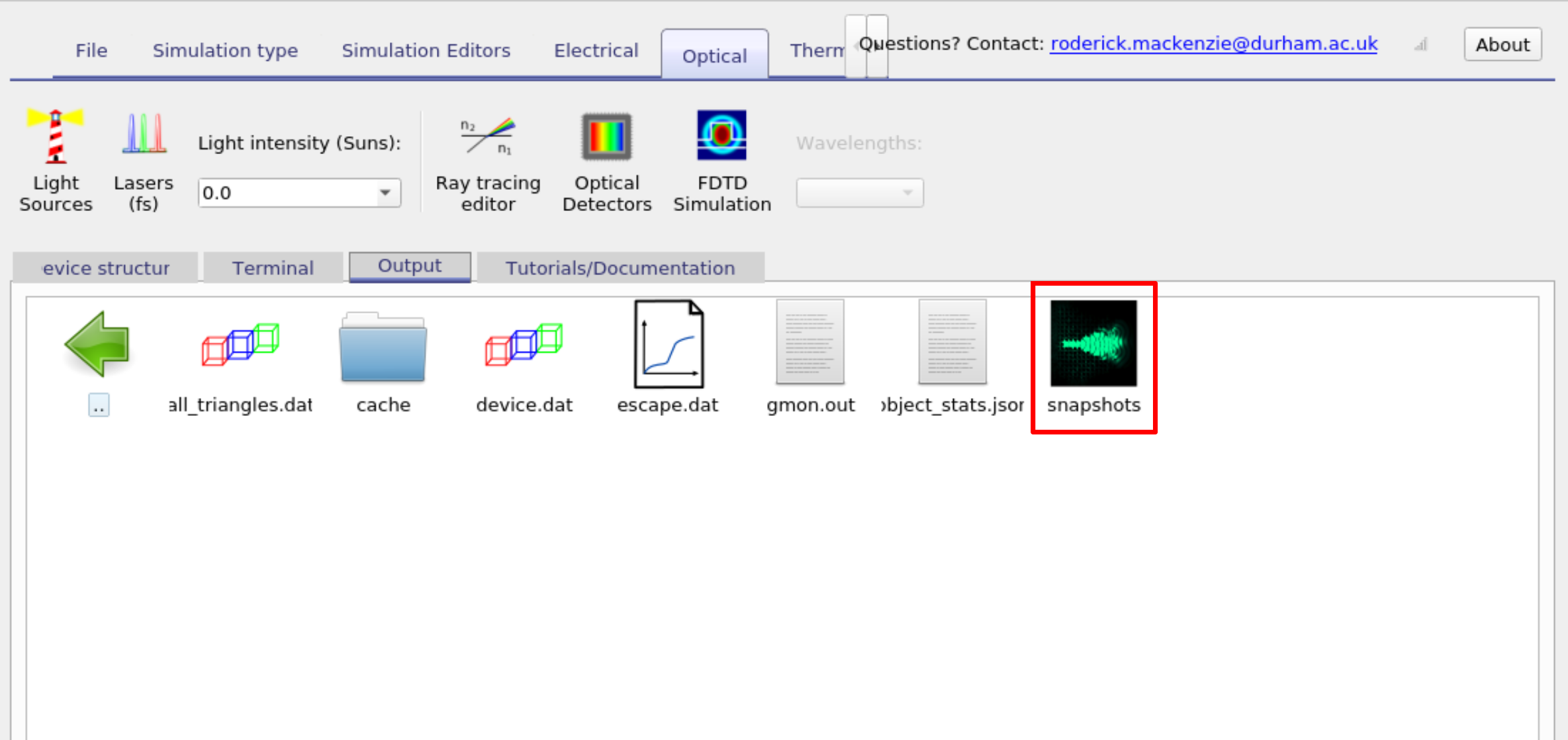
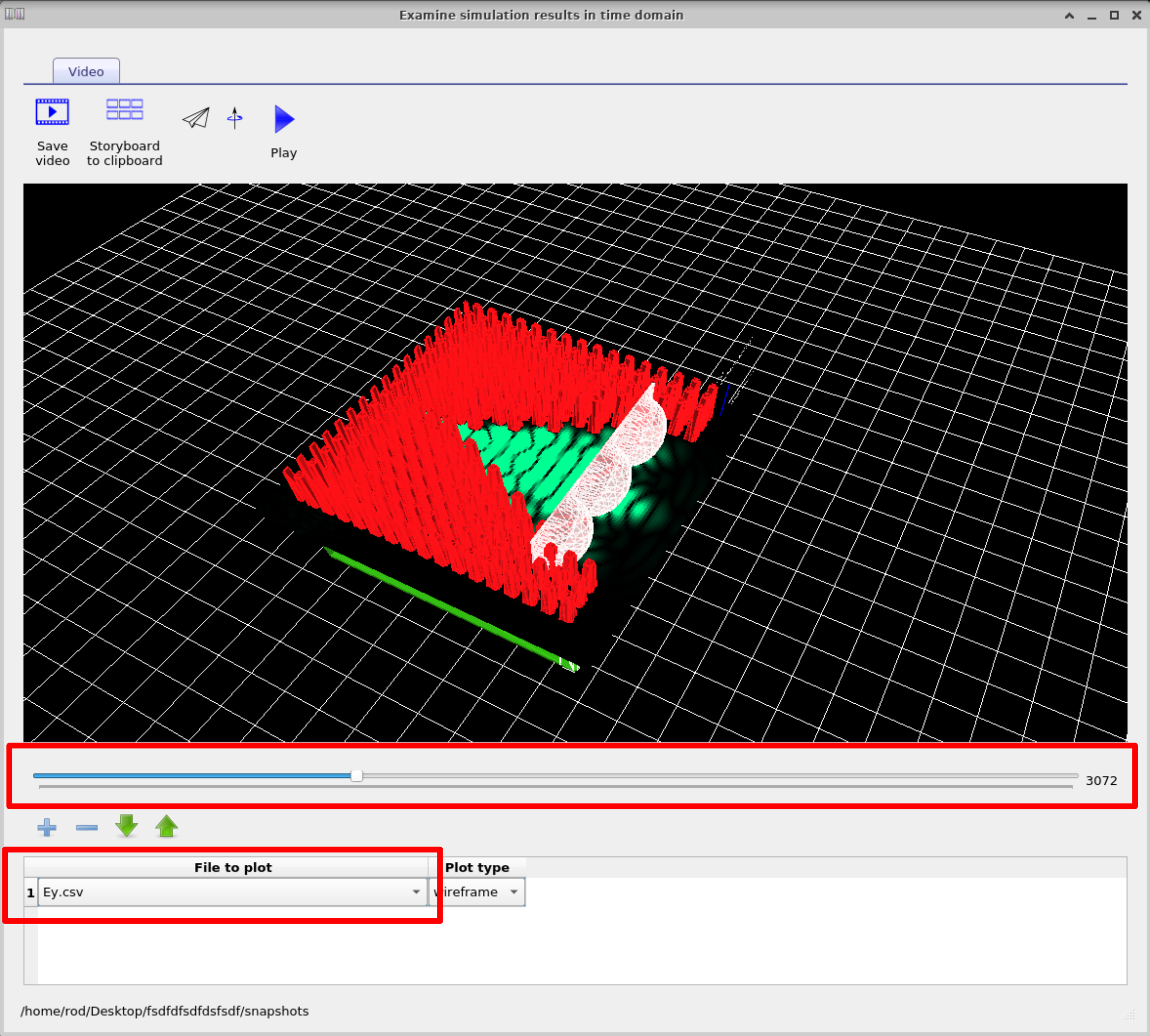
After the simulation has run click on the Output tab and 10.22 you will see the FDTD snapshots folder, this can be seen in figure 10.22. If you double click on this the FDTD snapshots window will appear which is shown in figure 10.23. This window will allow you to step through the simulations. If you click in the files to plot box, you will be able to select which field you plot. You will be able to select the Ey, Ex or Ez fields. In this case select the Ey field. Then use the slider bar to step through the field as a function of time.
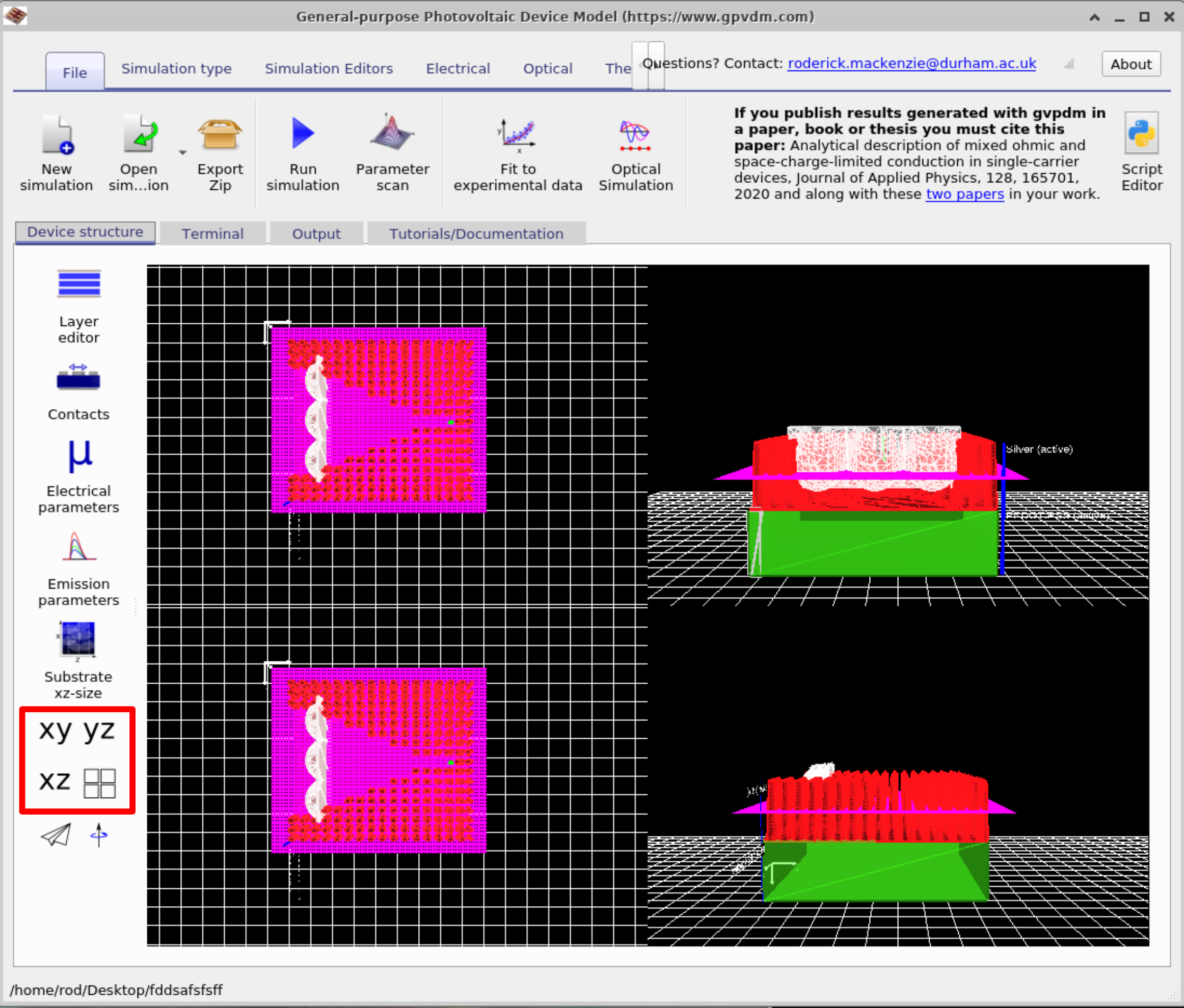
Manipulating objects in OghmaNano
Now close the snapshot viewer and go back to the main simulation window and select the Device tab. On the left of the window, you will see four buttons xy, yz, xz and for little square boxes this can be seen in figure 10.24. Try clicking them to see what happens to the view of the device. After you have had a play select the xz option, so that the screen looks like the left hand side of 10.26. If you left click on the lenses, you will notice that you will be able to move them around. Try to move the lenses back in the device so that your device looks more like the right hand side of figure 10.24. If you hold shift down while dragging an object you can rotate it on the spot.
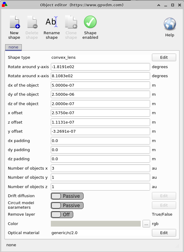
If you right click on the lenses and select Edit you will be able to bring up the object Editor. This shows the user all the object properties, this is visible in figure 10.27. Try changing the object type from \(convex\_lens\) to \(concave\_ lens\) by clicking the edit button and rerunning the simulation. If you want to add your own shapes to the shape data base see section 15.2. Using this window you can also change the material which is used in the FDTD simulation, the color of the object as well as its position or rotational angle.
The shape enabled button enables you to turn off the shape if you don’t want it in the simulation. If this shape were also electrically active you could also use this window to configure the electrical parameters.
 |
 |
Manipulating light sources in OghmaNano
Also visible in figure 10.26 is the light source given by the green arrow. Try moving this more forward in the device.
Theoretical background
References for this section are . This section of the manual aims to describe the FDTD code in full with verbose derivations to help understanding/pick up errors.
Ampere’s law is given as \[\sigma \boldsymbol{E} + \epsilon \frac{\partial \boldsymbol{E}}{\partial t} = \nabla \times \boldsymbol{H} = \begin{vmatrix} \hat{\boldsymbol{x}} & \hat{\boldsymbol{y}} & \hat{\boldsymbol{z}} \\ \frac{\partial}{\partial x} & \frac{\partial}{\partial y} & \frac{\partial}{\partial z} \\ H_{x} & H_{y} & H_{z} \end{vmatrix}\]
which can be expanded as
\[\sigma E_{x} + \epsilon \frac{\partial E_{x}}{\partial t} = \frac{\partial H_{z}}{\partial y}-\frac{\partial H_{y}}{\partial z}\]
\[\sigma E_{y} + \epsilon \frac{\partial E_{y}}{\partial t} = -\frac{\partial H_{z}}{\partial x}+\frac{\partial H_{x}}{\partial z}\]
\[\sigma E_{z} + \epsilon \frac{\partial E_{z}}{\partial t} = \frac{\partial H_{y}}{\partial x}-\frac{\partial H_{x}}{\partial y}\]
For the case \(\frac{\partial}{\partial y}=0\)
\[\begin{split} &\sigma E_{x} + \epsilon \frac{\partial E_{x}}{\partial t} =-\frac{\partial H_{y}}{\partial z}\\ &\sigma E_{y} + \epsilon \frac{\partial E_{y}}{\partial t} = -\frac{\partial H_{z}}{\partial x}+\frac{\partial H_{x}}{\partial z}\\ &\sigma E_{z} + \epsilon \frac{\partial E_{z}}{\partial t} = \frac{\partial H_{y}}{\partial x} \end{split}\]
for \(E_{x}\) \[\begin{split} &\sigma E_{x} + \epsilon \frac{\partial E_{x}}{\partial t} =-\frac{\partial H_{y}}{\partial z}\\ &\sigma \frac{E_{x}^{t+1}[]+E_{x}^{t}[]}{2} + \epsilon \frac{E_{x}^{t+1}[]-E_{x}^{t}[]}{\Delta t} = -\frac{H_{y}^{t+\frac{1}{2}}[\frac{1}{2}]-H_{y}^{t+\frac{1}{2}}[-\frac{1}{2}]}{\Delta z}\\ &\sigma \frac{E_{x}^{t+1}[]}{2} + \epsilon \frac{E_{x}^{t+1}[]}{\Delta t} = -\frac{H_{y}^{t+\frac{1}{2}}[\frac{1}{2}]-H_{y}^{t+\frac{1}{2}}[-\frac{1}{2}]}{\Delta z}-\sigma \frac{E_{x}^{t}[]}{2}+\epsilon \frac{E_{x}^{t}[]}{\Delta t}\\ &\sigma \frac{E_{x}^{t+1}[]}{2} + \epsilon \frac{E_{x}^{t+1}[]}{\Delta t} = -\frac{H_{y}^{t+\frac{1}{2}}[\frac{1}{2}]-H_{y}^{t+\frac{1}{2}}[-\frac{1}{2}]}{\Delta z}-\sigma \frac{E_{x}^{t}[]}{2}+\epsilon \frac{E_{x}^{t}[]}{\Delta t}\\ & \frac{\sigma \Delta t + 2 \epsilon }{ 2 \Delta t}E_{x}^{t+1}[] = -\frac{H_{y}^{t+\frac{1}{2}}[\frac{1}{2}]-H_{y}^{t+\frac{1}{2}}[-\frac{1}{2}]}{\Delta z}-\sigma \frac{E_{x}^{t}[]}{2}+\epsilon \frac{E_{x}^{t}[]}{\Delta t}\\ & E_{x}^{t+1}[] = \left ( -\frac{H_{y}^{t+\frac{1}{2}}[\frac{1}{2}]-H_{y}^{t+\frac{1}{2}}[-\frac{1}{2}]}{\Delta z}-\sigma \frac{E_{x}^{t}[]}{2}+\epsilon \frac{E_{x}^{t}[]}{\Delta t} \right ) \frac{2 \Delta t}{\sigma \Delta t + 2 \epsilon} \end{split}\]
for \(E_{y}\) \[\begin{split} &\sigma E_{y} + \epsilon \frac{\partial E_{y}}{\partial t} = -\frac{\partial H_{z}}{\partial x}+\frac{\partial H_{x}}{\partial z}\\ &\sigma \frac{E_{y}^{t+1}[]+E_{y}^{t}[]}{2} + \epsilon \frac{E_{y}^{t+1}[]-E_{y}^{t}[]}{\Delta t} = -\frac{H_{z}^{t+\frac{1}{2}}[\frac{1}{2}]-H_{z}^{t+\frac{1}{2}}[-\frac{1}{2}]}{\Delta x}+\frac{H_{x}^{t+\frac{1}{2}}[\frac{1}{2}]-H_{x}^{t+\frac{1}{2}}[-\frac{1}{2}]}{\Delta z}\\ &\sigma \frac{E_{y}^{t+1}[]}{2} + \epsilon \frac{E_{y}^{t+1}[]}{\Delta t} = -\frac{H_{z}^{t+\frac{1}{2}}[\frac{1}{2}]-H_{z}^{t+\frac{1}{2}}[-\frac{1}{2}]}{\Delta x}+\frac{H_{x}^{t+\frac{1}{2}}[\frac{1}{2}]-H_{x}^{t+\frac{1}{2}}[-\frac{1}{2}]}{\Delta z}-\sigma \frac{E_{y}^{t}[]}{2} + \epsilon \frac{E_{y}^{t}[]}{\Delta t}\\ &E_{y}^{t+1}[] = \left ( -\frac{H_{z}^{t+\frac{1}{2}}[\frac{1}{2}]-H_{z}^{t+\frac{1}{2}}[-\frac{1}{2}]}{\Delta x}+\frac{H_{x}^{t+\frac{1}{2}}[\frac{1}{2}]-H_{x}^{t+\frac{1}{2}}[-\frac{1}{2}]}{\Delta z}-\sigma \frac{E_{y}^{t}[]}{2} + \epsilon \frac{E_{y}^{t}[]}{\Delta t} \right ) \frac{2 \Delta t}{\sigma \Delta t + 2 \epsilon} \end{split}\]
for \(E_{z}\) \[\begin{split} &\sigma E_{z} + \epsilon \frac{\partial E_{z}}{\partial t} = \frac{\partial H_{y}}{\partial x}\\ &\sigma \frac{E_{z}^{t+1}[]+E_{z}^{t}[]}{2} + \epsilon \frac{E_{z}^{t+1}[]-E_{z}^{t}[]}{\Delta t} = \frac{H_{y}^{t+\frac{1}{2}}[\frac{1}{2}]-H_{y}^{t+\frac{1}{2}}[-\frac{1}{2}]}{\Delta x}\\ &\sigma \frac{E_{z}^{t+1}[]}{2} + \epsilon \frac{E_{z}^{t+1}[]}{\Delta t} = \frac{H_{y}^{t+\frac{1}{2}}[\frac{1}{2}]-H_{y}^{t+\frac{1}{2}}[-\frac{1}{2}]}{\Delta x}-\sigma \frac{E_{z}^{t}[]}{2} + \epsilon \frac{E_{z}^{t}[]}{\Delta t}\\ &E_{z}^{t+1}[]= \left ( \frac{H_{y}^{t+\frac{1}{2}}[\frac{1}{2}]-H_{y}^{t+\frac{1}{2}}[-\frac{1}{2}]}{\Delta x}-\sigma \frac{E_{z}^{t}[]}{2} + \epsilon \frac{E_{z}^{t}[]}{\Delta t} \right ) \frac{2 \Delta t}{\sigma \Delta t + 2 \epsilon}\\ \end{split}\]
Faraday’s law is given as \[-\sigma_{m} \boldsymbol{H} - \mu \frac{\partial \boldsymbol{H}}{\partial t} = \nabla \times \boldsymbol{E} = \begin{vmatrix} \hat{\boldsymbol{x}} & \hat{\boldsymbol{y}} & \hat{\boldsymbol{z}} \\ \frac{\partial}{\partial x} & \frac{\partial}{\partial y} & \frac{\partial}{\partial z} \\ E_{x} & E_{y} & E_{z} \end{vmatrix}\]
which can be expanded to give:
\[-\sigma_{m} H_{x} - \mu \frac{\partial H_{x}}{\partial t} = \frac{\partial E_{z}}{\partial y}-\frac{\partial E_{y}}{\partial z}\]
\[-\sigma_{m} H_{y} - \mu \frac{\partial H_{y}}{\partial t} = -\frac{\partial E_{z}}{\partial x}+\frac{\partial E_{x}}{\partial z}\]
\[-\sigma_{m} H_{z} - \mu \frac{\partial H_{z}}{\partial t} = \frac{\partial E_{y}}{\partial x}-\frac{\partial E_{x}}{\partial y}\]
With \(\sigma_m=0\) and \(\frac{\partial}{\partial y}=0\)
\[\begin{split} &\frac{\partial H_{x}}{\partial t} = \frac{1}{\mu} \left ( \frac{\partial E_{y}}{\partial z} \right )\\ &\frac{\partial H_{y}}{\partial t} = \frac{1}{\mu} \left ( \frac{\partial E_{z}}{\partial x}-\frac{\partial E_{x}}{\partial z} \right )\\ &\frac{\partial H_{z}}{\partial t} = - \frac{1}{\mu} \left ( \frac{\partial E_{y}}{\partial x} \right ) \end{split}\]
which discretizing gives
\[\begin{split} & H_{x}^{t+1} = \frac{1}{\mu} \left ( \frac{E_{y}^{t+\frac{1}{2}}[\frac{1}{2}]-E_{y}^{t+\frac{1}{2}}[-\frac{1}{2}]}{\Delta z} \right ) \Delta t + H_{x}^{t}[]\\ & H_{y}^{t+1} = \frac{1}{\mu} \left ( \frac{E_{z}^{t+\frac{1}{2}}[\frac{1}{2}]-E_{z}^{t+\frac{1}{2}}[-\frac{1}{2}]}{\Delta x}-\frac{E_{x}^{t+\frac{1}{2}}[\frac{1}{2}]-E_{x}^{t+\frac{1}{2}}[-\frac{1}{2}]}{\Delta z} \right ) \Delta t+ H_{y}^{t}[]\\ & H_{z}^{t+1} = \frac{1}{\mu} \left ( - \frac{E_{y}^{t+\frac{1}{2}}[\frac{1}{2}]-E_{y}^{t+\frac{1}{2}}[-\frac{1}{2}]}{\Delta x} \right ) \Delta t + H_{x}^{z}[] \end{split}\]
Ray tracing model
Add text.