Simulation modes and simulation editors
OghmaNano uses a modular architecture that enables the core solver to perform a variety of simulation types using . For example there is a plugin to perform steady state JV simulations, another plugin to perform frequency domain simulations, and another to calculate the Quantum Efficiency. They all leverage the same OghmaNano core solver but run it in a slightly different way with custom inputs and outputs. A list of the plugins and what they do can be found below:
-
Plugins for various types of experiment
- jv – Calculate steady-state JV curves.
- suns_jsc – Simulate suns vs. Jsc curves.
- suns_voc – Suns vs. Voc simulations.
- eqe – Simulate EQE.
- cv – Capacitance–voltage simulations.
- ce – Simulate charge extraction experiments.
- time_domain – Time-domain solver for transient simulations.
- fx_domain – Simulate frequency-domain response (electrical and optical excitation).
- pl_ss – Calculate PL spectrum in steady state.
- mode – Solve optical modes in 1D/2D waveguides.
- spm – Simulate scanning probe microscopy in 3D electrical simulations.
- equilibrium – Equilibrium electrical simulations.
- exciton – Exciton simulations.
- mesh_gen – Generate meshes.
-
Optical solver plugins
- fdtd – Finite Difference Time Domain (FDTD) optical solver.
- optics – Optical transfer matrix solver for 1D structures.
- light_full – Optical transfer matrix solver.
- light_qe – Calculate optical profile using experimental quantum efficiency.
- light_exp – Calculate optical profile assuming exponential light propagation in 1D structures.
- light_flat – Calculate optical profile assuming flat profiles in the structure.
- light_constant – Use user-given generation rates in optical structures.
- light_fromfile – Load generation rate from a file.
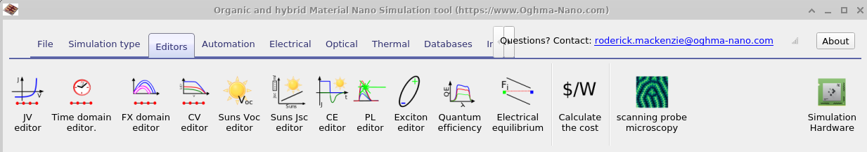
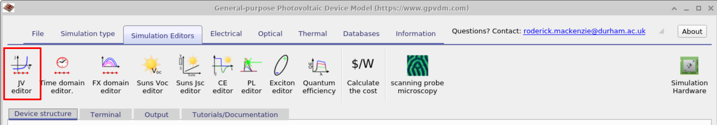
In the simulation editors ribbon (see Figure 4.1) you can see icons that represent each plugin, these are the simulation editors. By
clicking on an icon in this ribbon you will be able to edit how the plugin performs the various simulations. For
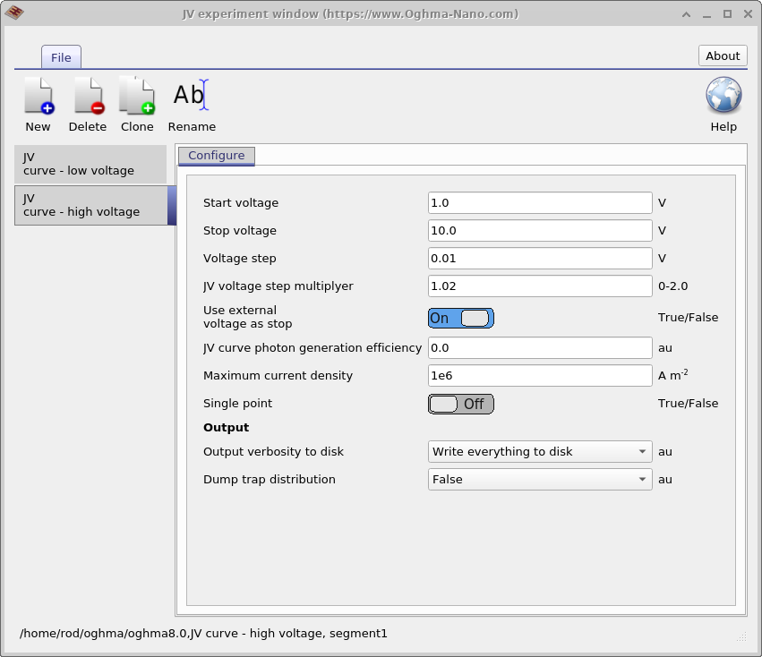
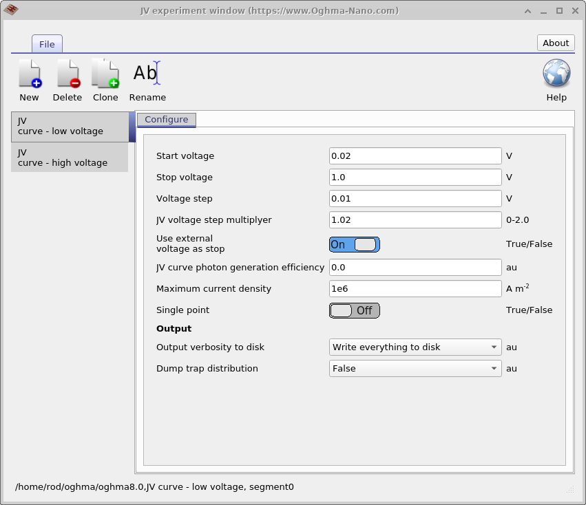
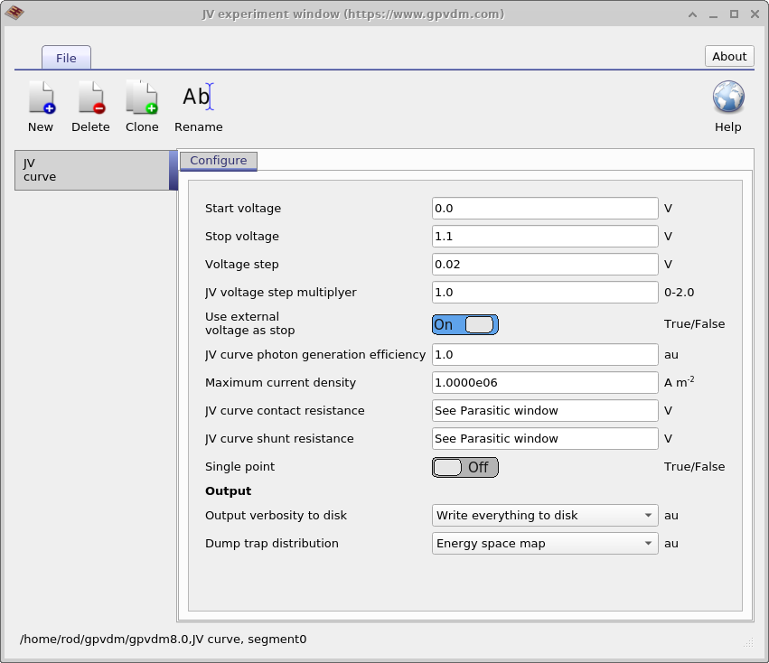
example in the JV simulation editor one can change the start/stop voltages of a voltage sweep. The JV editor can be
seen in Figure [fig:jv_low]. Within
each simulation editor the user can define multiple so called experiments. This can be seen in below in
Figure [fig:jv_low] and Figure
[fig:jv_high], where two JV scans
have been defined within the JV editor, one called JV curve - low voltage and another called JV curve
- high voltage. One has a start voltage of 0.02V and stop voltage of 1.0V, while the other has a start voltage
of 1.0V and a stop voltage of 10V. This feature is most useful in more complex experiments such as in time domain
experiments where one may want to simulate multiple different voltage/light ramps/pulses for one device. There is
no limit to how many experiments can be defined for each plugin.
 [fig:jv_low]
 [fig:jv_high]
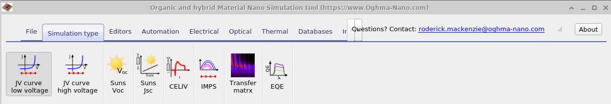
Once an experiment has been defined an icon representing it will appear in the simulation mode ribbon shown in figure 4.2. You can see in the figure an icon for JV curve low voltage and JV curve high voltage that were defined in Figure [fig:jv_low] and [fig:jv_high]. You can see in Figure 4.2 that JV curve low voltage is depressed. This means that when the simulation is run this simulation mode will be executed. If you select another simulation mode, then when the play button (or F9) is pressed that simulation mode will be run. Only one simulation mode can be run at a time.
JV editor (Steady state simulation editor)
If you click on the JV editor icon in figure 4.3, the JV editor window will open shown below in figure 4.4.
Inputs
This window can be used to configure steady state simulations. It does not matter if you are running a current-voltage sweep on a solar cell or an OFET. This plugin will steadily ramp the voltage from a start voltage to a stop voltage. The voltage will be applied to the contact which has been set to Change in the contact editor (see section 3.1.8). You can set the start voltage, stop voltage and step size. Use JV voltage step multiplayer to make the voltage step grow each step. The default is 1.0, i.e. no growth. It can be helpful to set the step multiplyer to a value larger than 1.0 if you want to speed up the simulation but it should not be increased past about 1.05 or the simulation may strugle to converge.
Outputs
The files produced by the JV simulation mode are given in table 10.1. As well as these files, by default OghmaNano will also write all internal simulation parameters to disk in the snapshots directory. This includes band structure, potential, carrier distributions, generation rates etc.. this equates to about 50 files per voltage step. You can read more about this in the simulation snapshots section, see 19.1. This can considerably slow down the simulation, the user can therefore decide how much is written to disk by using the Output verbosity to disk option this can be set to; Key results, which will result in only key files being written to disk;Nothing, which will result in no results being written to disk; Write everything to disk which will result in a all possible information being written to disk and Write everything to disk every nth step, which will only out comprehensive internal simulation write data every nth step.
| File name | Description | Notes |
|---|---|---|
charge.dat |
Charge density vs. voltage | |
jv.dat |
Current–voltage curve | |
k.csv |
Recombination constant k | |
sim_info.dat |
Simulation summary (calculated \(V_{oc}\), \(J_{sc}\), etc.); see §4.1.4 |
sim_info.dat
This is a json file containing all key simulation metrics such as \(J_{sc}\), \(V_{oc}\), and example sim_info.dat file is given below:
Steady state electrical simulation
In steady state electrical simulations such as performing a JV scan the sim_info.dat outputs the following parameters.
| Symbol | JSON token | Meaning | Units | Equ. | Ref |
|---|---|---|---|---|---|
| \(FF\) | ff | Fill factor | au | ||
| \(PCE\) | pce | Power conversion efficiency | % | ||
| \(P_{max}\) | P_max | Power at maximum power point | W | ||
| \(V_{oc}\) | V_oc | Open-circuit voltage | V | ||
| \(voc_{R}\) | voc_R | Recombination rate at \(P_{max}\) | |||
| \(jv_{voc}\) | jv_voc | JV data point at \(V_{oc}\) | |||
| \(jv_{pmax}\) | jv_pmax | JV data point at \(P_{max}\) | |||
| \(voc_{nt}\) | voc_nt | Trapped electron density at \(V_{oc}\) | m\(^{-3}\) | ||
| \(voc_{pt}\) | voc_pt | Trapped hole density at \(V_{oc}\) | m\(^{-3}\) | ||
| \(voc_{nf}\) | voc_nf | Free electron density at \(V_{oc}\) | m\(^{-3}\) | ||
| \(voc_{pf}\) | voc_pf | Free hole density at \(V_{oc}\) | m\(^{-3}\) | ||
| \(J_{sc}\) | J_sc | Short-circuit current density | A m\(^{-2}\) | ||
| \(jv_{jsc}\) | jv_jsc | Average charge density at \(J_{sc}\) | m\(^{-3}\) | ||
| \(jv_{vbi}\) | jv_vbi | Built-in voltage | V | ||
| \(jv_{gen}\) | jv_gen | Average generation rate | |||
| \(voc_{np}\) | voc_np | Carrier density product at \(V_{oc}\) | |||
| \(j_{pmax}\) | j_pmax | Current at \(P_{max}\) | A m\(^{-2}\) | ||
| \(v_{pmax}\) | v_pmax | Voltage at \(P_{max}\) | V |
| Symbol | JSON token | Meaning | Units | Equ. | Ref |
|---|---|---|---|---|---|
| \(\mu_{jsc}\) | mu_jsc | Avg. mobility at \(J_{sc}\) | m\(^2\) V\(^{-1}\) s\(^{-1}\) | ||
| \(\mu^{geom}_{jsc}\) | mu_geom_jsc | Geom. avg. mobility at \(J_{sc}\) | m\(^2\) V\(^{-1}\) s\(^{-1}\) | ||
| \(\mu^{geom\_micro}_{jsc}\) | mu_geom_micro_jsc | Geom. micro avg. mobility at \(J_{sc}\) | m\(^2\) V\(^{-1}\) s\(^{-1}\) | ||
| \(\mu_{voc}\) | mu_voc | Avg. mobility at \(V_{oc}\) | m\(^2\) V\(^{-1}\) s\(^{-1}\) | ||
| \(\mu^{geom}_{voc}\) | mu_geom_voc | Geom. avg. mobility at \(V_{oc}\) | m\(^2\) V\(^{-1}\) s\(^{-1}\) | \(\sqrt{\langle\mu_e\rangle \langle\mu_h\rangle}\) | |
| \(\mu^{geom\_avg}_{voc}\) | mu_geom_micro_voc | Geom. micro avg. mobility at \(V_{oc}\) | m\(^2\) V\(^{-1}\) s\(^{-1}\) | \(\langle\sqrt{\mu_e \mu_h}\rangle\) | |
| \(\mu^e_{pmax}\) | mu_e_pmax | Avg. electron mobility at \(P_{max}\) | m\(^2\) V\(^{-1}\) s\(^{-1}\) | ||
| \(\mu^h_{pmax}\) | mu_h_pmax | Avg. hole mobility at \(P_{max}\) | m\(^2\) V\(^{-1}\) s\(^{-1}\) | ||
| \(\mu^{geom}_{pmax}\) | mu_geom_pmax | Geom. avg. mobility at \(P_{max}\) | m\(^2\) V\(^{-1}\) s\(^{-1}\) | \(\sqrt{\langle\mu_e\rangle \langle\mu_h\rangle}\) | |
| \(\mu^{geom\_micro}_{pmax}\) | mu_geom_micro_pmax | Geom. micro avg. mobility at \(P_{max}\) | m\(^2\) V\(^{-1}\) s\(^{-1}\) | \(\langle\sqrt{\mu_e \mu_h}\rangle\) | |
| \(\mu_{pmax}\) | mu_pmax | Avg. mobility at \(P_{max}\) | m\(^2\) V\(^{-1}\) s\(^{-1}\) |
| Symbol | JSON token | Meaning | Units | Equ. | Ref |
|---|---|---|---|---|---|
| \(\tau_{voc}\) | tau_voc | Recombination time at \(V_{oc}\) | s | \(R=(n-n_0)/\tau\) | |
| \(\tau_{pmax}\) | tau_pmax | Recombination time at \(P_{max}\) | s | \(R=(n-n_0)/\tau\) | |
| \(\tau^{all}_{voc}\) | tau_all_voc | Recombination time (all carriers) at \(V_{oc}\) | s | \(R=n/\tau\) | |
| \(\tau^{all}_{pmax}\) | tau_all_pmax | Recombination time (all carriers) at \(P_{max}\) | s | \(R=n/\tau\) | |
| \(\theta_{srh}\) | theta_srh | \(\theta_{SRH}\) Collection coefficient at \(P_{max}\) | au | p.100 5.2a |
Time domain editor
Related YouTube videos:
 |
Simulating optoelectronic sensors made from polymers. |
The time domain editor can be used to configure time domain simulations, this is shown in Figure 4.6. You can see, as described in the previous section that one simulation editor can be used to edit multiple experiments. The panel on the left shows the editor being used to edit a CELIV simulation while the panel on the right shows the editor being used to edit a TPC simulation. The new, delete and clone buttons in the top of the window can be used to make new simulation modes. The table in the bottom of the window can be used to setup the time domain mesh, apply voltages or light pulses.
 |
 |
Figure 4.8 shows different tabs in of the time domain editor. The image on the left shows the circuit diagram used to model the CELIV experiment. The diode on the left represents the drift diffusion simulation while the other components represent various parasitic components. After the diode from the left next comes a capacitor used to model the charge on the plates of the device, then a shunt resistance and then the series resistance. The final resistor on the right represents the external resistance of the measuring equipment, this is by default set to zero but worth checking. The drop down menu on the top left of the image above the circuit diagram says load type, this can change the load the circuit from what is shown in the picture, to a perfect diode where no parasitic components are shown to a device at open circuit which would be used to simulate Transient Photo Voltage measurements. The right hand figure shows the configuration options of the time domain window. Again notice the Output verbosity to disk option as described in the previous section, you will see this again and again in OghmaNano.
 |
 |
Frequency domain editor
Related YouTube videos:
|
Simulating impedance spectroscopy (IS) in solar cells. |
Overview
The frequency plugin allows you to simulate the frequency domain response of the device. Using this tool one can
perform impedance spectroscopy, as well as optically excited measurements such as Intensity Modulated Photo
Spectroscopy (IMPS), Intensity Modulated Voltage Spectroscopy (IMVS). The domain editor allows you to configure
frequency domain simulations. This is shown below in Figures [fig:fx_domain_mesh] and [fig:fx_domain_circuit]. On the
left hand side is the frequency domain mesh editor this is used to define which frequencies will be simulated.
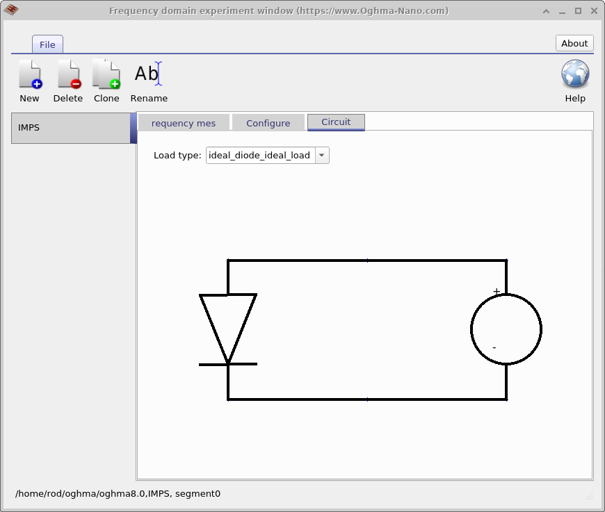
Figure [fig:fx_domain_circuit] shows the circuit tab of the frequency domain window,
this sets the electrical configuration of the simulation. One can either simulate an ideal diode (this is the
fastest type of simulation to perform), a diode with parasitic components or a diode in open circuit. An ideal
diode would be used for IMPS simulations while the open circuit model would be used for IMVS simulations. Pick the
circuit depending on what conditions you want to simulate. If you want examples of frequency domain simulation look
in the new simulation window under Organic Solar cells, some of the PM6:Y6 devices have examples of frequency
domain simulations already set up.
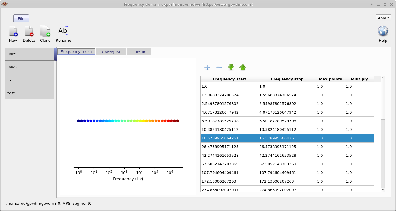 [fig:fx_domain_mesh]
 [fig:fx_domain_circuit]
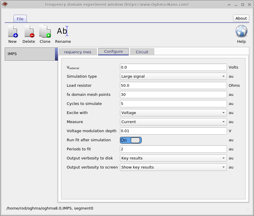
Large signal or small signal
There are two ways to simulate frequency domain simulations in a device model, a large signal approach or a small signal approach. The small signal approach assumes the problem we are looking at varies linearly around a DC point, this may or may not be true depending on the conditions one is looking at. This method is however computationally fast. The second approach is to use a large signal approach and rather than simulating linear variation around a set point one simulates the time domain response of the device in full for each wavelength of interest. This method is cope better non-linear systems and one does not need to worry if one is in the large or small signal regime but is slower. OghmaNano uses the large signal approach.
Inputs
In Figure 4.9 the Configure tab of the frequency domain window can be seen. This decides exactly how the simulation will perform. These are described below in table 4.2
| File name | Description |
|---|---|
| Cycles to simulate | The number of complete periods of any given frequency that are simulated. |
| Excite with | How the device is excited, either optically or electrically. |
| FX domain mesh points | The number of time steps used to simulate each cycle. |
| Load resistor | External load resistor, usually set to zero. |
| Measure | What is measured, current or voltage. |
| Modulation depth | How deep the DC voltage/current is modulated. |
| Output verbosity to disk | How much data is dumped to disk (described in other sections). |
| Output verbosity to screen | How much data is shown on the screen (described in other sections). |
| Periods to fit | The number of frequency domain cycles that are fit to extract phase angle. |
| Simulation type | Leave this as Large signal. |
| \(V_{external}\) | The external voltage applied to the cell. |
Outputs
| File name | Description | Notes |
|---|---|---|
| fx_abs.csv | fx vs. \(\lvert i(fx) \rvert\) | |
| fx_C.csv | fx vs. Capacitance | |
| fx_imag.csv | fx vs. Im(i(fx)) | |
| fx_phi.csv | fx vs. \(\angle i(fx)\) | |
| fx_R.csv | fx vs. Resistance | |
| fx_real.csv | fx vs. Re(i(fx)) | |
| real_imag.csv | Re(i(fx)) vs. Im(i(fx)) |
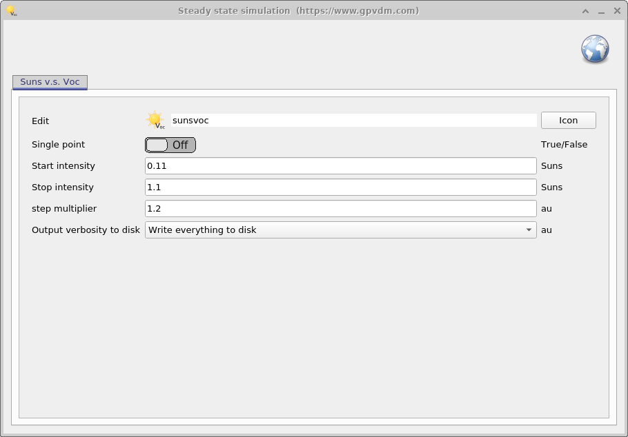
Suns-Voc editor
The Suns-Voc plugin can be used to calculate how open circuit voltage changes as a function of light intensity. This can be useful for understanding tail slope and disorder in devices. A picture of the suns-voc editor window can be seen below in figure 4.10. The window can be used to set the start and stop light intensity. The Suns-Voc applies the voltage to the contact that is labelled Change.
Outputs
| File name | Description |
|---|---|
| Q_kbi.csv | Charge density vs. recombination prefactor kbi |
| Q_mu.csv | Charge density vs. charge carrier mobility |
| Q_Qtau.csv | Charge density vs. recombination constant tau |
| Q_trap_filling.csv | Charge density vs. fraction of filled traps |
| suns_mu.csv | Suns vs. average charge carrier mobility |
| suns_Q.csv | Suns vs. Charge density |
| suns_tau.csv | Suns vs. recombination constant tau |
| suns_voc.csv | Suns vs. Voc curve |
| V_mu.csv | Voc vs. average charge carrier mobility |
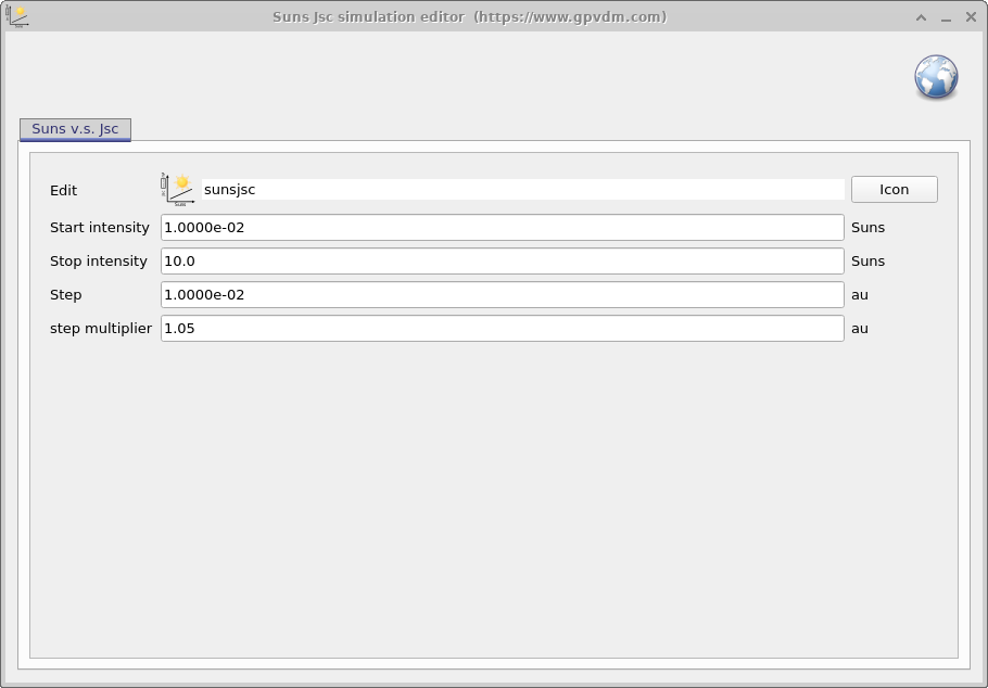
Suns-Jsc editor
The Jsc editor can be used to configure suns-Jsc simulations. It enables you to set the start light intensity, stop light intensity and how big the steps are. This is shown in figure 4.11.
Outputs
| File name | Description |
|---|---|
| suns_jsc.csv | Suns vs. Jsc curve |
| suns_mu.csv | Suns vs. average charge carrier mobility |
Quantum efficiency editor
The quantum efficiency editor simulates both EQE and IQE. The configuration window can be used to set the voltage at which EQE and IQE are performed.
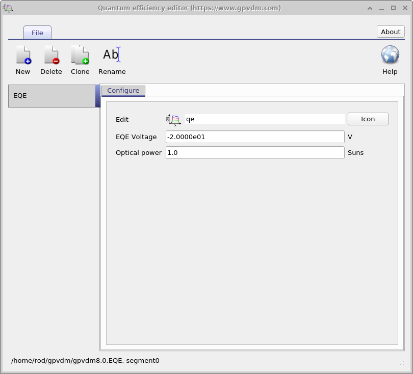
Outputs
| File name | Description |
|---|---|
| E_eqe.csv | Photon energy vs. EQE |
| E_eqe_norm.csv | Photon energy vs. Normalized EQE |
| E_iqe.csv | Photon energy vs. IQE |
| eqe.csv | Wavelength vs. EQE |
| iqe.csv | Wavelength vs. IQE |
| lam_Gn.csv | Wavelength vs. Average charge carrier generation rate |
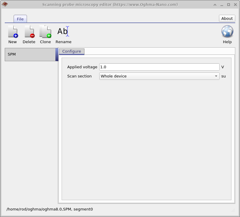
Scanning probe microscopy editor
When simulating a 3D structure such as a large area contact one often wants to map the resistance between an x,z point on the surface of the device and the charge extraction contact. This tool is used to apply voltages systematically over z,x regions to map out voltage or resistance profiles in space. This tool is usually used with either full 2/3D drift diffusion simulations or the 3D large area electrical circuit model. There is more about this tool in Section 12.
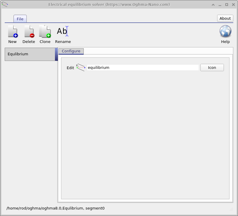
Electrical equilibrium editor
Sometimes when studding a device, it is not necessary to simulate an entire JV curve. One may for example just for example be interested in the band structure at 0V in the dark. The Electrical equilibrium allows the user to setup simulations that only simulate the device at equilibrium (0V applied bias in the dark).
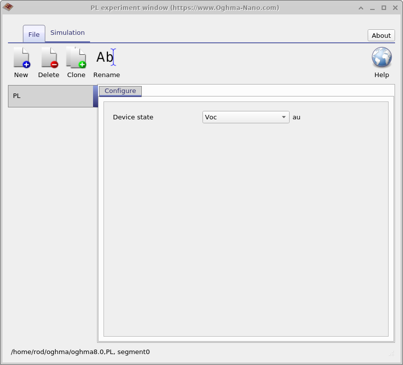
Steady state photoluminencense editor
This tool is used to generate photoluminencense spectra at a desired voltage, either short circuit or open circuit.
Charge extraction editor
This is the charge extraction editor, it allows one to simulate charge extraction transients. A charge extraction experiment is performed to find out how much charge is in a disordered device. For this type of experiment one runs the device at a set voltage and light intensity say 1V @ 1Sun. Then one turns off the light and shorts the cell through a resistor and integrates the total current outputted by the cell to get the charge that was in the cell when it was operating. Typically the cell is shorted through the the 50 Ohm termination of an oscilloscope so that by measuring the voltage transient and applying V=IR one can calculate the current and thus total charge.
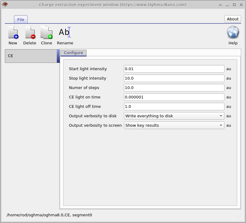 [fig:ce_editor]
This type of measurement is important in disordered devices when one wants to find out how much charge is in the
trap states. It is important to note that the experiment does not extract all the charge in the device, it only
extracts the difference between charge at operating conditions and 0V @ 0 Suns. The background charge due to
injection from the contacts/doping is still left in the device. There is also error loss in the CE experiment due
to recombination annihilating charge before it has left the device.
Outputs
| File name | Description | Notes |
|---|---|---|
| suns_np.dat | Suns vs. extracted charge including the effects of recombination | |
| suns_np_ideal.dat | Suns vs. extracted charge not including the effects of recombination | |
| suns_Q_ce.dat | Suns vs. extracted charge including effects of recombination | |
| time_i.csv | Time vs. extraction current for a single CE experiment | |
| time_v.csv | Time vs. voltage for a single CE experiment | |
| v_np.dat | Voltage vs. extracted charge including the effects of recombination | |
| v_np_ideal.dat | Voltage vs. extracted charge not including the effects of recombination |
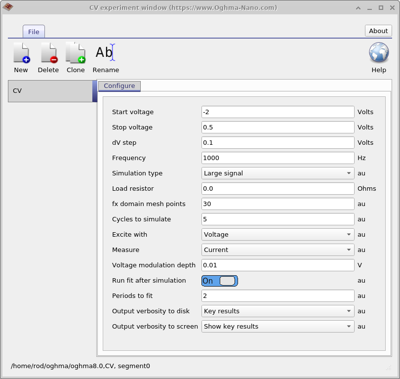
Capacitance voltage editor
Experimentally capacitance voltage (CV) measurements are a useful way to determine doping within a device. In OghmaNano CV measurements use a cut down version of frequency domain simulation tool described above.
Outputs
| File name | Description |
|---|---|
| cv.dat | fx vs. Capacitance |
| cv2.dat | fx vs. \(1/\text{Capacitance}^2\) |
| fx_imag.dat | fx vs. Im(i(fx)) |
| fx_real.dat | fx vs. Re(i(fx)) |
| real_imag.dat | Re(i(fx)) vs. Im(i(fx)) |
Hardware editor
All computer programs including OghmaNano run on physical computing hardware. There are may combinations of hardware that can be in any computer, some computes have a large number of CPU cores while others only have one. Likewise computers come with differing amounts of memory, hard disk space and GPUs. To help the user get the best out of OghmaNano, there is a hardware editor where the user can configure how OghmaNano behaves on any given computer. This can be accessed through the simulation tab window see Figure 4.17.
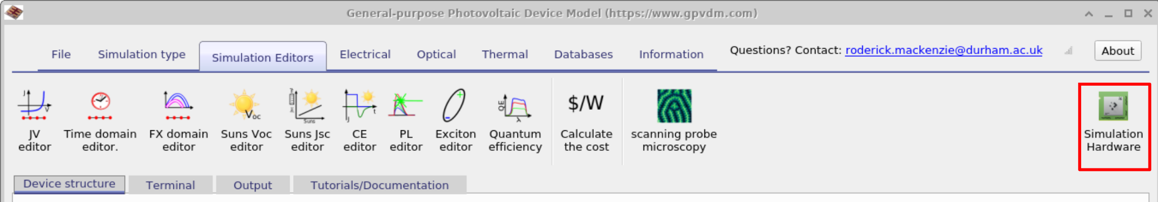
If you click on this it will bring up the hardware editor window which can be seen in Figure 4.18
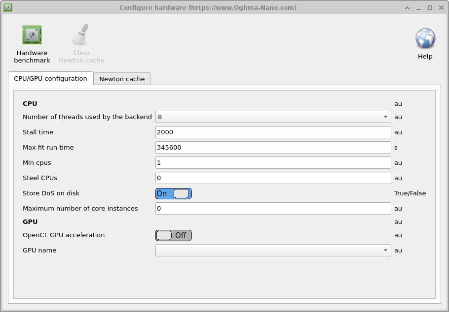
The hardware window is comprised of various tabs which enable the user to edit the configuration and also benchmark your device.
CPU/GPU configuration tab
This tab is used to configure how OghmaNano interacts with the GPU and CPU it is described in the table below. As described in other parts of this manual in detail there are two parts to OghmaNano there is oghma_core.exe which is the computational back end and there is oghma_gui.exe which is the graphical user interface, how both these parts of the model behave can be fine tuned here.
-
Number of threads used by the backend: This is the maximum number of threads OghmaNano oghma_core.exe can use. This dictates; the number of simultaneous fits that can be run; the maximum number of optimization simulations that can be run at the same time; the maximum number of threads that are used for FDTD simulations; maximum number of of DoS cache files can generated at the same time; number of frequency domain points that can be run at the same time.
-
Maximum number of core instances: This sets the maximum number of oghma_core.exe instances that can be started by the GUI. If one is running a parameter scan then this will control the maximum number of simultaneous simulations that can be performed at the same time. If the values of Number of threads used by the backend has been set to 4 and one is performing an FDTD simulation, then one sets Maximum number of core instances to 8, then the GUI will spawn 8 instances of oghma_core.exe each using 4 threads, thus 32 CPU cores will be needed.
-
Stall time: Sometimes when running OghmaNano on a supercomputer unattended it can stop running, possibly because of an IO error or network error. This option can be used to set the maximum length of a single simulation. By single simulation I mean a single JV curve, single time domain simulation or single frequency domain simulation, but not a whole fit which will involve running thousands if individual simulations.). So with a value of 2000 seconds the solver will exit, if for example a single JV simulation takes longer than 2000 seconds. In reality any individual simulation should take only a few seconds, so this option acts as a hard backstop if something has gone very wrong.
-
Max fit run time: This is the maximum time oghma_core.exe can reside in memory. If any simulation or fit takes longer than this value it will be terminated, again this is a backstop to prevent simulations running forever. The default value is 4 days.
-
Steel CPUs: Sometimes when running OghmaNano on a shared PC one will set a simulation running when another user is using a significant number of cores. After a while the other user’s simulations will finish running leaving the computer with idling CPUs. If this option is set to True, then OghmaNano will monitor the number of free CPUs and if more become available it will use them.
-
Min CPUs: Used with the option above Steel CPUs to set the minimum number of CPUs that will be used.
-
Store DoS on disk: OghmaNano stores lookup tables on disk to speed up simulations, if this option is set to false these lookup tables will not be stored.
-
OpenCL GPU acceleration: This enables or disables GPU acceleration, this is used mainly during the FDTD simulations.
-
GPU name: Selects the GPU to use.
Newton cache
When running simulations with a significant number of ODEs, such as 1D devices with a lot of trap states and a lot of spatial points, or when running 2D OFET simulations each voltage step can take a while to compute. This is because the solver must solve each voltage step using Newton’s method until it converges. For each each solver step the Jacobian must be built, the matrix inverted multiplied by the residuals and updates to all solver variables calculated. This can take a significant amount of time per step (2000ms). An approach to side step this approach is to store previously calculated answers on disk and then when the user asks the solver to calculated an already calculated problem the answer can be recalled rather than recalculated. This is very useful in OLED design where one is trying to optimise the optical structure of the device but leaves the electrical structure unchanged. One can run new optical simulations with already pre-calcualted electrical solutions. Configuration options are displayed in the table below.
There is an overhead to using the Newton Cache, so I would only recommend it when solving the electrical problem
is very slow indeed. Technically the Newton cache works by taking the MD5 sum of the Fermi-levels and the
potentials to generate a hash of the electrical problem. This is then compared to what exists on disk. If a
precalculated answer is found, the Fermi-levels/potentials are updated to the values found on disk. The cache is
stored in oghma_local
cache, each pre solvedsolution is stored as a new binary file. Each simulation run generates an index file where
all MD5 sums from that simulation are stored. Once the cache becomes full OghmaNano deletes simulation results in
batches based on the index files.
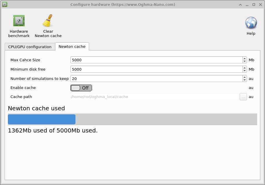
-
Maximum cache size: Sets the maximum size of the cache in Mb. I would recommend around 1Gb.
-
Minimum disk free: Sets the minimum amount of disk space needed to use the cache, this option is designe dto prevent the cache filling the disk I would set it to around 5Gb.
-
Number of simulations to keep: This will set the maximum number of simulation runs to keep, I would set it to between 20 and 100.
-
Enable cache: This enables or disables the Newton Cache, the default and recommended option is False.
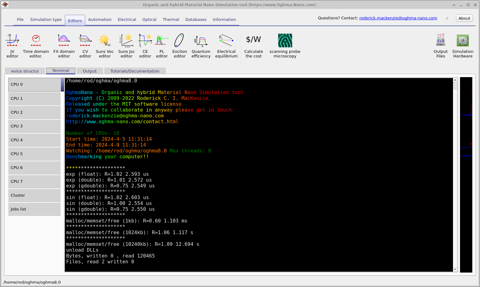
Hardware benchmark
In the top left of hardware window 4.19 there is a button called Hardware benchmark. If this is clicked then OghmaNano will benchmark your hardware, the result of such a benchmark can be seen in 4.20. This runs benchmarks your CPUs ability to calculate sin,exp and allocate/deallocate memory in blocks. It displays how long it took to do a few thousand operations as well as an R (aka Roderick) value. This is defined as R=Time taken to do the calculation on your PC/The time take to do the calculation on my PC. Thus smaller values mean your PC is faster than mine. My PC is a Intel(R) Core(TM) i7-4900MQ CPU @ 2.80GHz in a 2017 Lenovo thinkpad. So most modern computers should be faster. If you have good CPU performance but your simulations are running slower than my YouTube videos then this is invariably due to bad IO speed, caused by virus killers, storing the simulations on OneDrive, using networked drives, using slow USB storage etc.