|
|
|
|
|
|
OghmaNano provides a physics-based silicon simulation environment spanning crystalline silicon junction devices, MOS electrostatics, and thin-film amorphous silicon solar cells. Rather than treating silicon as a single generic material, the software lets you choose the level of physics appropriate to the problem: full drift–diffusion + Poisson transport for junction devices, electrostatic gate control for MOS capacitors, and coupled optical + electrical modelling for illuminated thin-film structures.
This makes OghmaNano useful both for teaching canonical semiconductor physics and for research-scale device analysis. You can study how a doping profile sets the built-in field in a PN junction, how a gate voltage bends the bands in silicon at a SiO2 interface, or how defect-mediated recombination limits the voltage of an amorphous silicon solar cell. If you want a broader overview of the solver stack, see the drift–diffusion examples page and the drift–diffusion theory section.
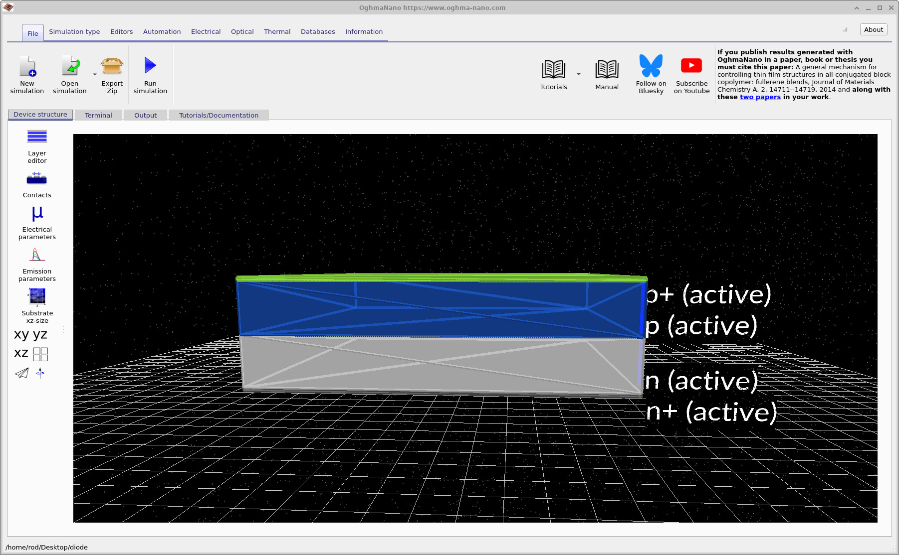
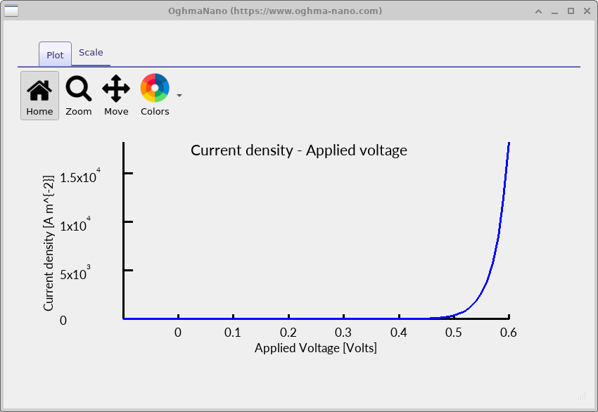
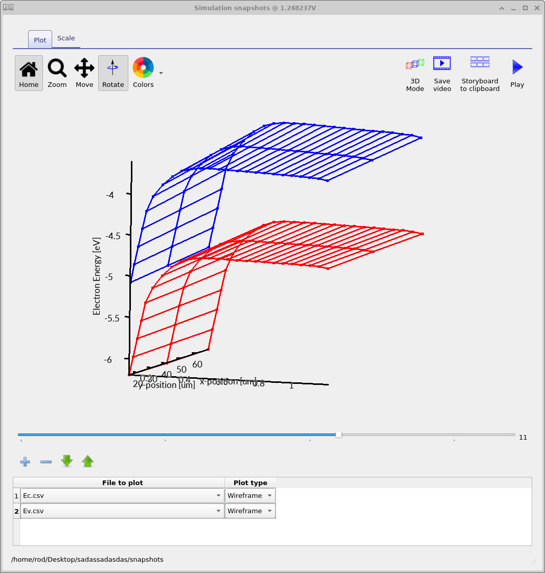
For crystalline silicon devices, OghmaNano resolves the coupled drift–diffusion and Poisson equations directly. This allows you to move beyond ideal diode equations and inspect the internal physics: the depletion region, band bending, electron and hole currents, and how SRH and Auger recombination modify the dark I–V curve.
This workflow is particularly useful for understanding how silicon junction behaviour depends on doping, lifetime, injection level, and contact-region design. In the silicon PN junction tutorial, OghmaNano is used to inspect how recombination remains localised near the junction at low bias and spreads more broadly through the device at high forward injection. It also links neatly back to the general drift–diffusion landing page and the more detailed theory pages on SRH and Auger physics.
Start here: Silicon PN junction diode tutorial.
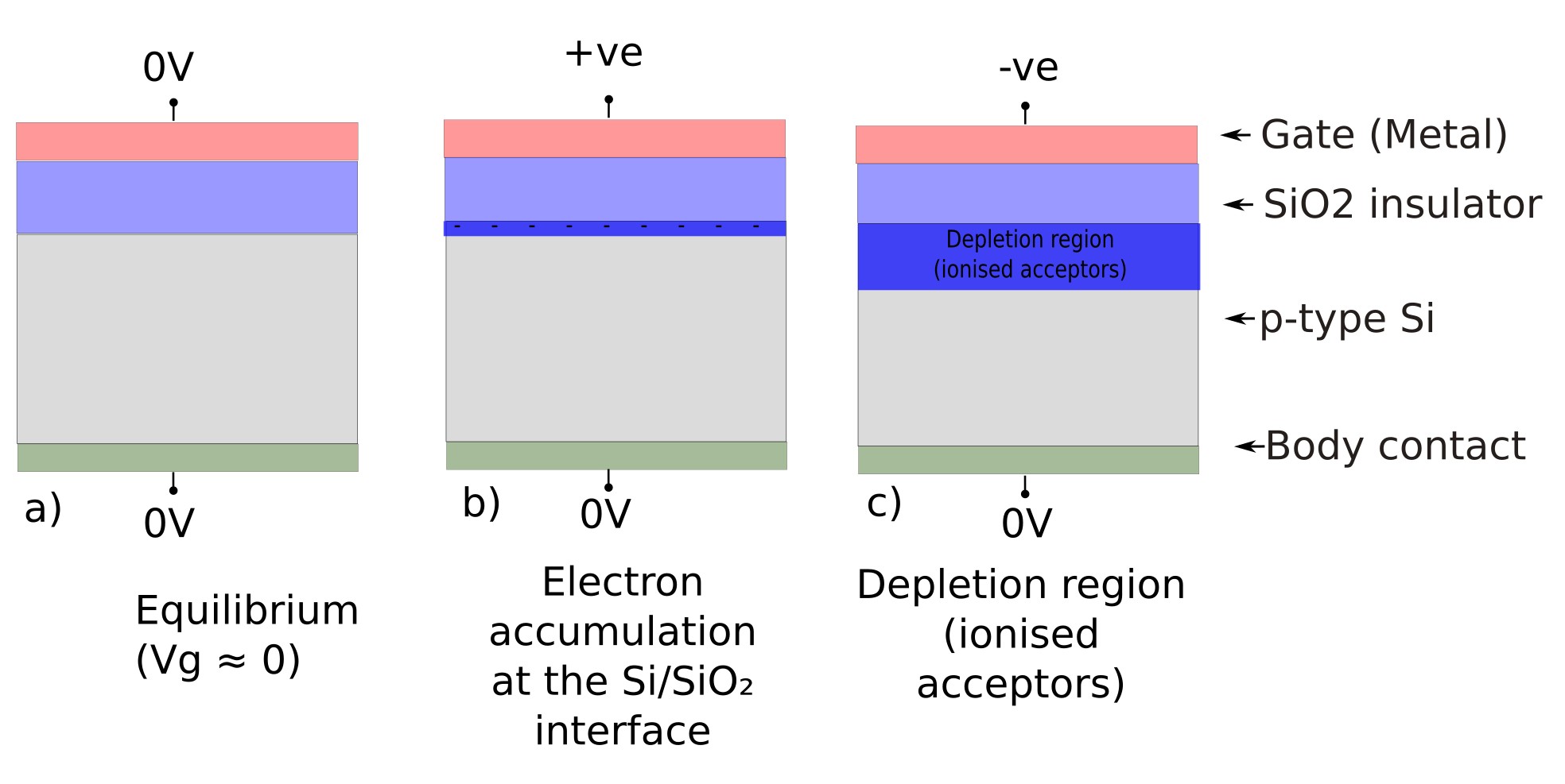
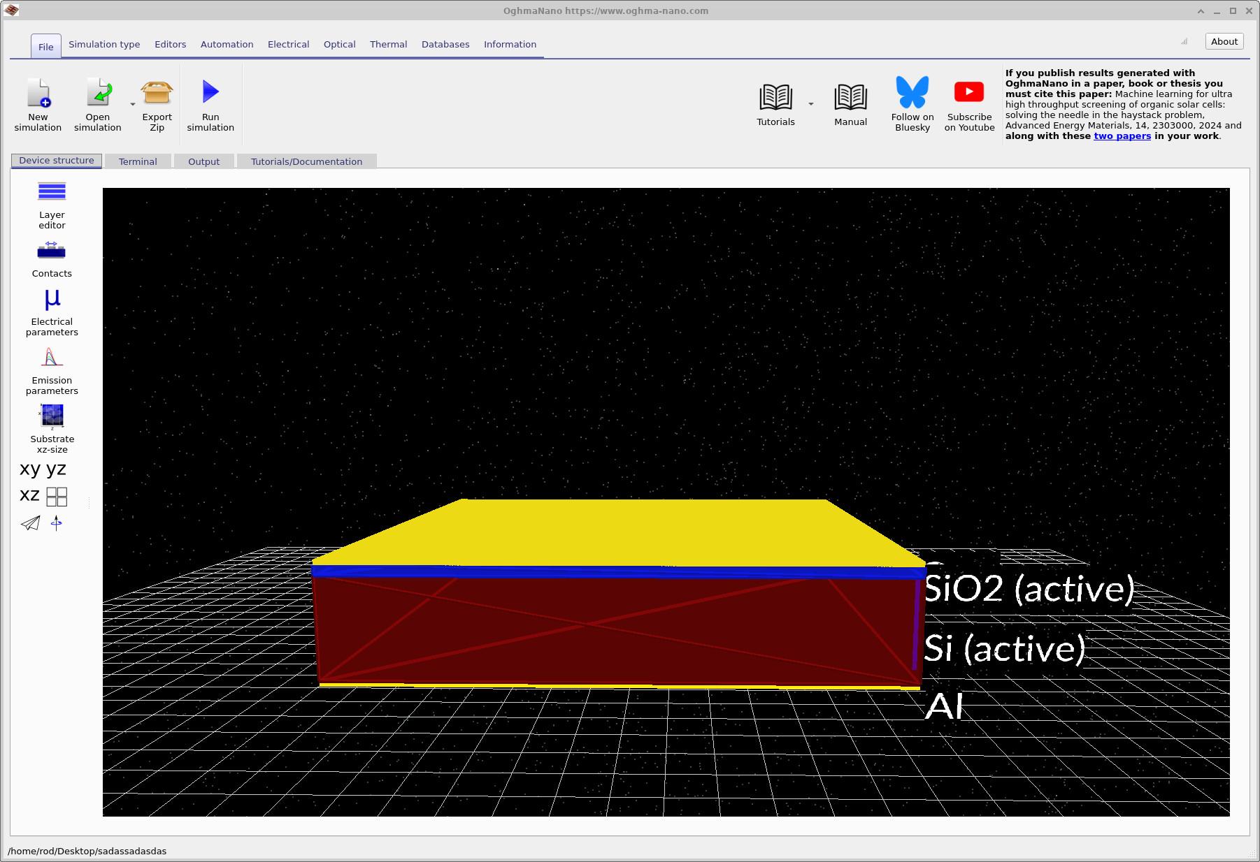
OghmaNano can also model MOS capacitor electrostatics, making it easy to teach and explore the basic physics behind NMOS operation. In this workflow, the oxide is treated as an insulating dielectric and the silicon as the mobile-carrier region, so you can examine how the applied gate voltage divides between the oxide and semiconductor, and how that drives surface accumulation or depletion.
This is a clean route into silicon device physics because the results map directly onto textbook concepts: surface potential, band bending, free carrier density near the interface, and the distinction between electrostatic control and current-carrying transport. The NMOS capacitor examples are especially useful for lectures, labs, and self-study, and they connect naturally to the broader semiconductor transport framework.
Start here: NMOS capacitor tutorial – Part A and Part B.
OghmaNano also supports hydrogenated amorphous silicon (a-Si:H) device modelling, where the dominant limitations are very different from crystalline silicon. In thin-film a-Si:H, carrier mobilities are lower, disorder is stronger, and recombination is typically controlled by defect-mediated SRH processes. The built-in field is established across an intrinsic absorber layer, and optical generation must be solved together with the electrical problem.
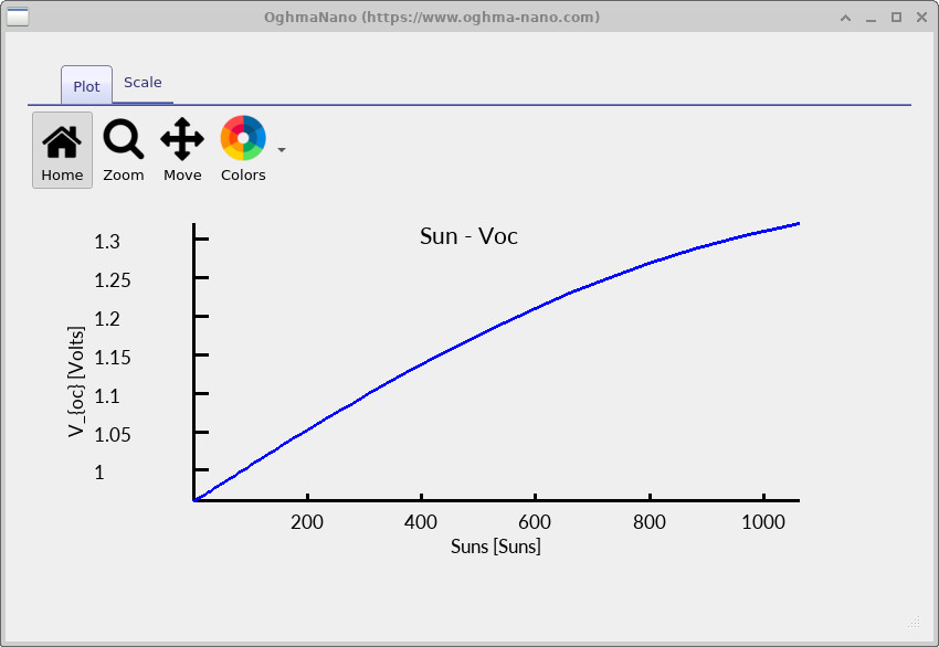
This makes a-Si:H a very useful reference case for studying recombination-limited photovoltage, optical generation in thin absorbers, and Suns–Voc behaviour. OghmaNano can calculate the generation profile using the transfer-matrix optical solver, feed it into the electrical model, and then extract the resulting JV and open-circuit-voltage behaviour. For the underlying trap physics, see also why traps are needed in disordered semiconductors and non-equilibrium SRH theory.
Start here: Amorphous silicon (a-Si:H) solar cell tutorial.
Want to dive deeper?
👉 Start with the silicon PN junction tutorial, explore MOS capacitor electrostatics, jump to amorphous silicon solar-cell modelling, or browse the general drift–diffusion examples.