Simulating Bulk-Heterojunction Morphologies with 2D Electrical Slices
https://doi.org/10.4208/cicp.OA-2022-01151. Introduction
Bulk-heterojunctions (BHJs) are the workhorse microstructure for many organic electronic devices—most famously organic solar cells, but also photodetectors, sensors, and other mixed ionic–electronic systems where percolating pathways and local bottlenecks matter. In a BHJ, two phases interpenetrate on the 10–100 nm scale, creating a large internal interface and a transport landscape that is fundamentally not one-dimensional. The trade-off is complexity: once you resolve the microstructure you inevitably inherit percolation limits, dead-ends, constrictions, and strong spatial variation in carrier density and recombination. For most day-to-day device fitting, you would not start here. You would typically work at the 1D device level—fast, robust, and often entirely appropriate—possibly including additional physics such as trapping and recombination. For example, the OPV quick-start tutorial demonstrates a standard 1D workflow (including trap physics where required) that is the right tool for the majority of routine studies and parameter extraction.
At the other end of the abstraction ladder, if your goal is system-level questions such as scaling, series/shunt losses, or module/panel behaviour, you would normally move to a large-area / circuit-aware description rather than resolving nanoscale morphology. The large-area PM6:Y6 tutorial is an example of that higher-level modelling approach.
This tutorial deliberately goes in the opposite direction: it keeps the microstructure (via an explicit BHJ morphology) but remains computationally practical by solving the electrical problem on 2D slices. The point is not that every device should be fit this way; it is that having a microstructure-resolving workflow is scientifically and technologically valuable. It lets you stress-test effective-medium assumptions, see where “simple” models break down, and build intuition for morphology-driven limits on performance—particularly when percolation and spatially localised trapping/recombination dominate.
2. Create a morphology simulation and inspect the BHJ
From the main window, click New simulation. This opens the device-type library shown in ??. Double-click Morphology, then save the project somewhere on your local disk. Saving locally matters because morphology-resolved simulations can generate many intermediate files (meshes, snapshots, caches), and local storage is typically much faster and more reliable than network or cloud-synchronised folders.
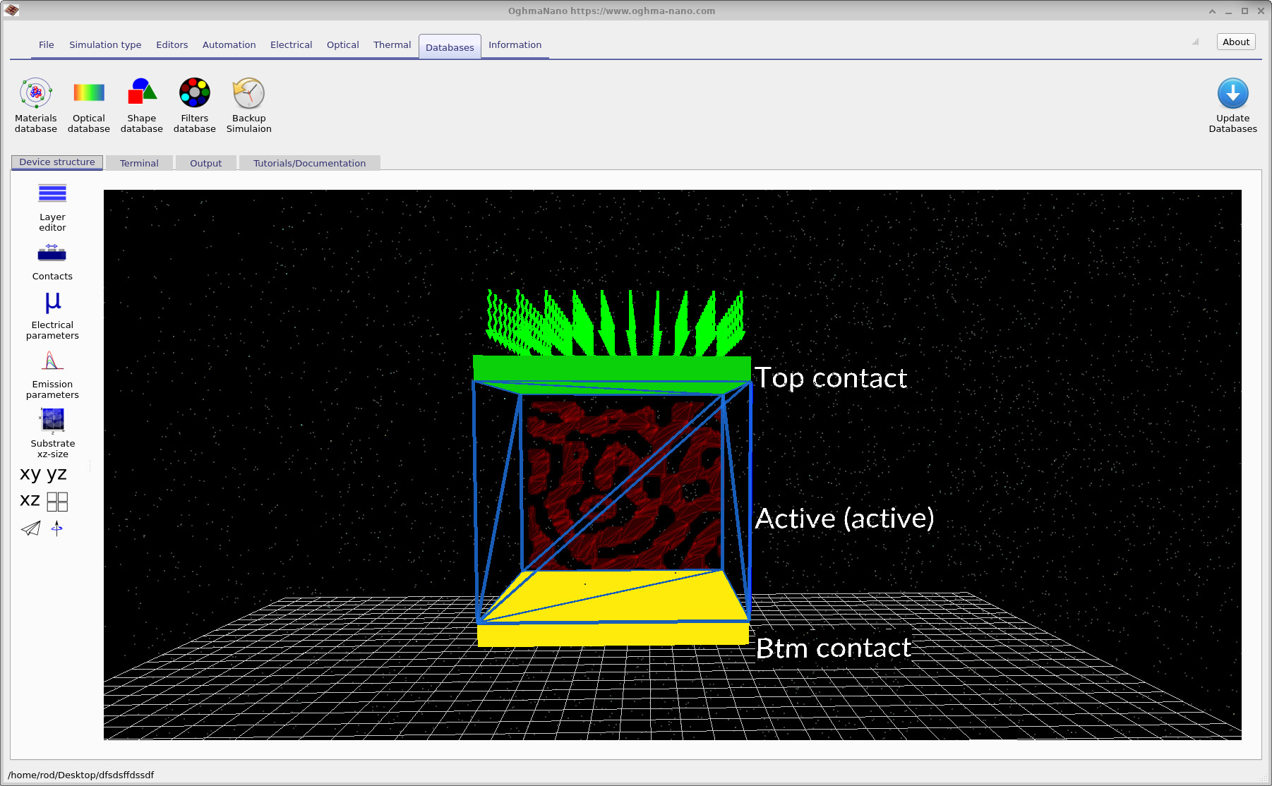
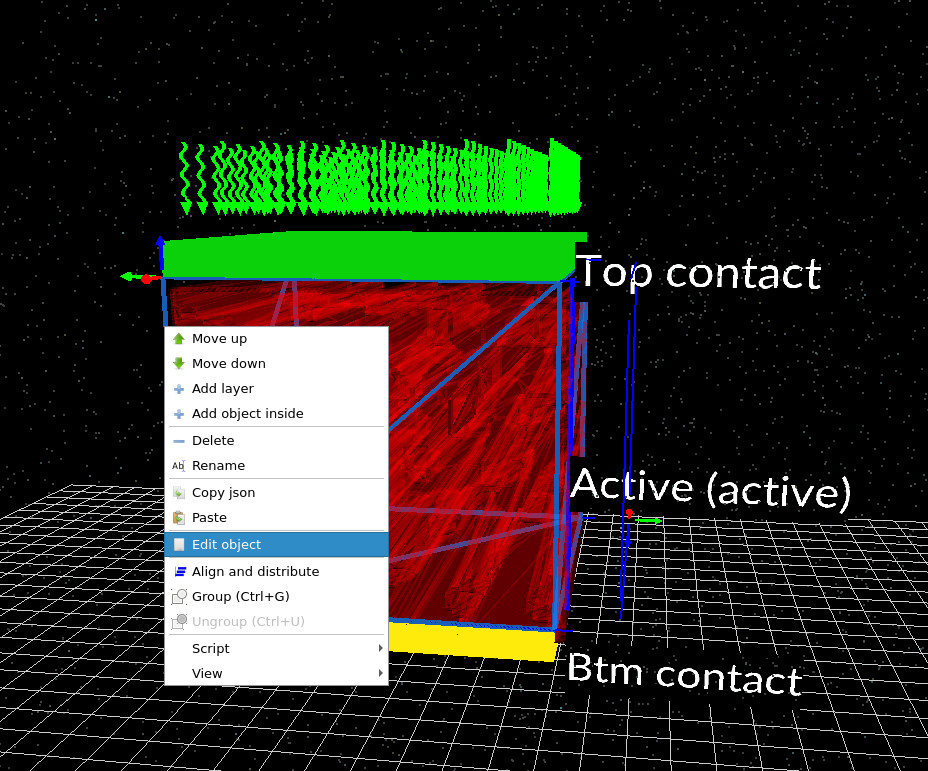
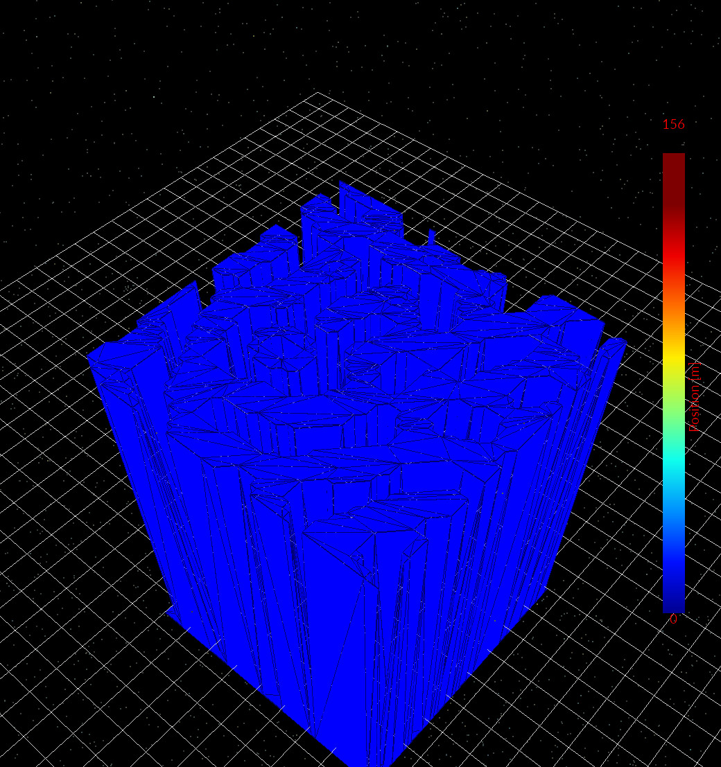
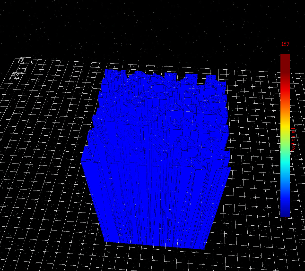
After creating the project, the main device window opens. You should see a central red object representing one phase of the bulk-heterojunction (BHJ), embedded inside the enclosing active layer region, as shown in ??. While the full 3D view is informative, morphology can be visually dense. To make the internal structure clearer, right-click the BHJ object and select View → Show cut through Y.
Enabling the cut-through view produces the rendering shown in ??, which exposes a 2D slice through the 3D morphology. This makes it much easier to see phase connectivity, interfaces, and percolation pathways within the BHJ.
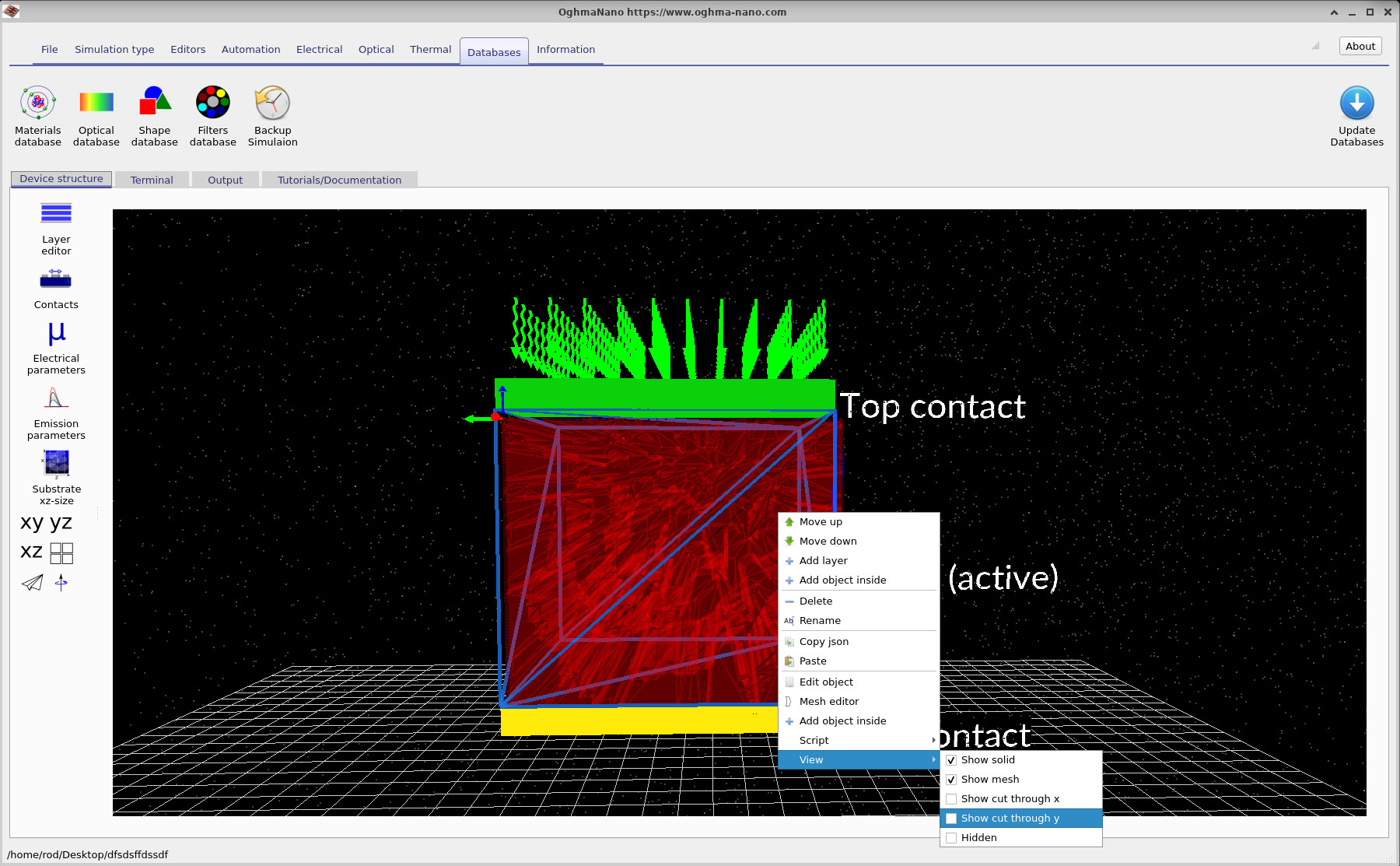
A useful mental model at this stage is the following: the enclosing rectangular region defines the active layer volume, while the embedded red object defines one explicit BHJ phase (for example, the polymer). The complementary phase is implicitly defined as the remainder of the active layer volume not occupied by the embedded object. This separation becomes explicit when examining object properties in the object editor in the following sections.
3. Device structure: active layer and embedded BHJ morphology
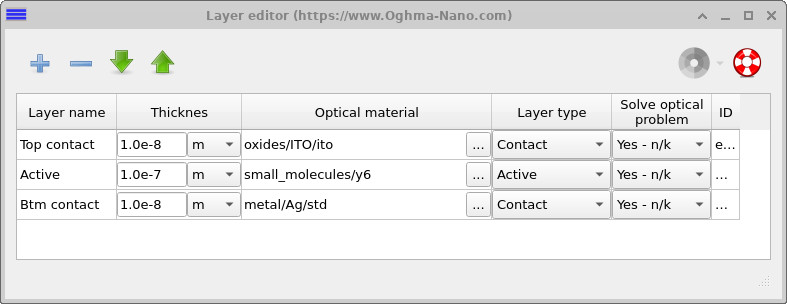
Open the Device structure tab and click Layer editor. The device consists of three layers: a top contact, a single active layer, and a bottom contact (Figure ??). This deliberately simple stack makes it easier to understand how morphology enters the electrical problem, without introducing additional interfaces or transport layers. The key point is that the active layer itself is a simple rectangular volume defined in the layer editor. In this example it is assigned the molecular material Y6 an acceptor, and-on its own-it is just a box. All of the structural complexity associated with the bulk-heterojunction is introduced separately, by embedding a second object inside this active-layer volume. That embedded object is a complex CAD mesh imported from the Shape database, represents the PM6 polymer phase. The polymer mesh defines a closed three-dimensional volume inside the active layer. The complementary phase (the acceptor-rich region) is then defined implicitly as the part of the active layer that is not occupied by the polymer mesh. In other words, the BHJ is represented by volume exclusion rather than by explicitly defining two interlocking meshes.
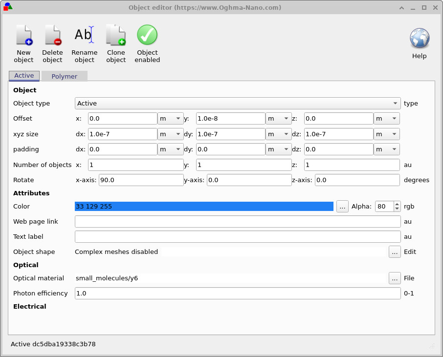
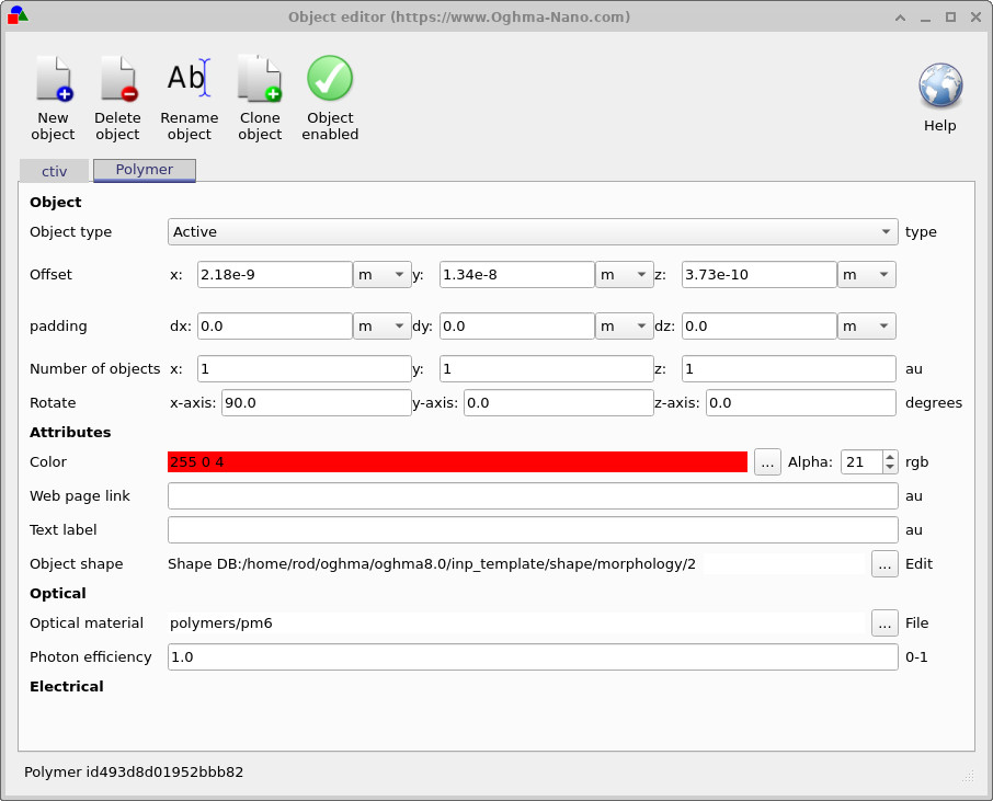
This separation becomes clear when inspecting the objects in the 3D view. There are two relevant objects: the enclosing active-layer box (typically shown as a blue wireframe), and the embedded polymer morphology (shown in red). To inspect their properties, right-click the blue enclosing region and select Edit object, as shown in ??.
In the object editor, the distinction is explicit. For the enclosing Active object, the Object shape is a simple box (with complex meshes disabled). For the Polymer object, the Object shape points to a Shape DB entry, which is the triangulated mesh defining the PM6 morphology. Switching this reference swaps the polymer morphology while leaving the surrounding active layer unchanged.
This construction—simple active-layer box plus embedded polymer volume—is central to how BHJ morphologies are handled in OghmaNano. It makes the geometry easy to reason about, ensures the polymer phase forms a well-defined closed region, and allows you to study how percolation, connectivity, and constrictions in the polymer network influence charge transport once the electrical solver is run.
4. Electrical parameters: mobilities and SRH trap bands
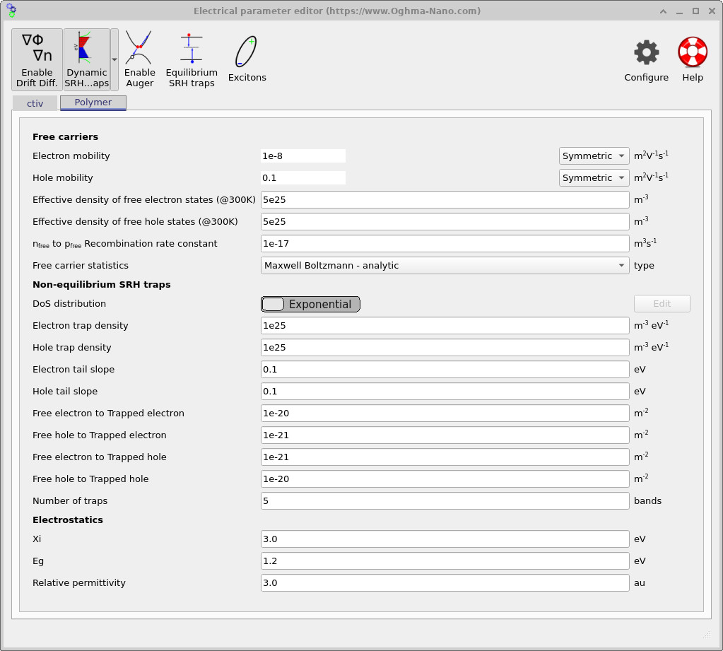
Open the Electrical parameters editor from the main window. Separate parameter panels are provided for the two phases of the active layer: the enclosing Active region (acceptor / matrix) and the embedded Polymer morphology, shown in ?? and ??. This is where the two interpenetrating phases are made electrically distinct.
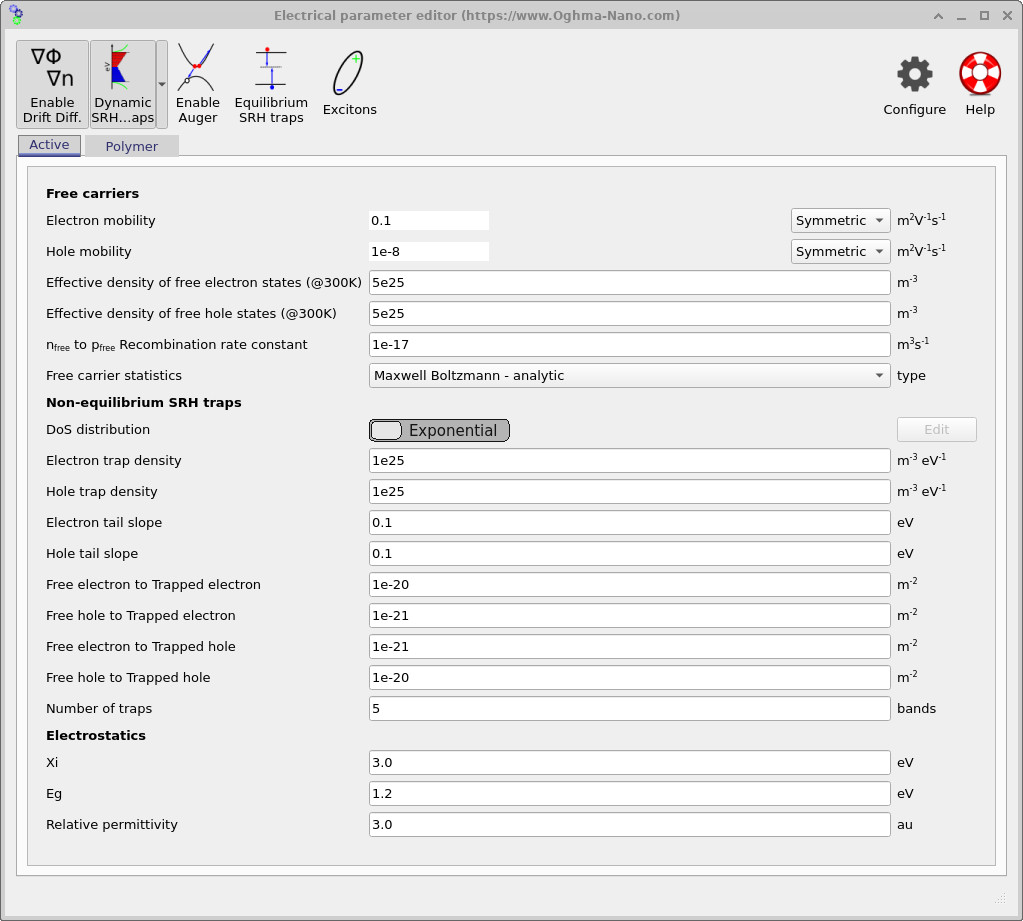
Both phases use the same basic transport formalism: drift–diffusion with Maxwell–Boltzmann carrier statistics and symmetric mobility tensors. The key difference is the intentional mobility contrast. In the polymer phase, the hole mobility is high while the electron mobility is suppressed; in the complementary active phase, this is reversed. This enforces selective transport: holes percolate through the polymer network, while electrons percolate through the matrix.
This simple asymmetry is enough to generate physically meaningful BHJ behaviour. Even before running the simulation, it defines what you should expect to see in the spatial outputs: continuous percolation pathways, dead-ends where carriers become trapped geometrically, and local charge build-up at constrictions or poorly connected regions of the morphology. In addition to free-carrier transport, non-equilibrium Shockley–Read–Hall (SRH) trapping is enabled in both phases. As shown in the parameter panels, the density of states is represented using exponential tail distributions for both electrons and holes, with identical trap densities and energetic slopes in each phase. The solver tracks five discrete trap bands at every mesh point.
Each trap band exchanges carriers dynamically with the free populations through explicit capture and emission terms (free-to-trapped coupling constants visible in the editor). As a result, the system being solved includes not only free electron and hole densities, but also multiple trapped carrier populations at every spatial location. This substantially increases numerical stiffness and computational cost, but is essential for capturing dispersive transport, trap-assisted recombination, and realistic transient behaviour in disordered organic semiconductors. The numerical values used here are intended as a stable, illustrative example rather than a calibrated material model. Once the workflow is understood, these parameters can be refined, validated against experiment, or simplified if the goal is to isolate morphology and percolation effects rather than trapping physics.
5. Meshing
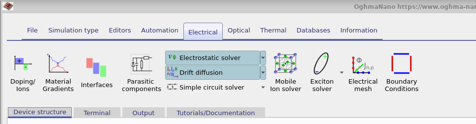
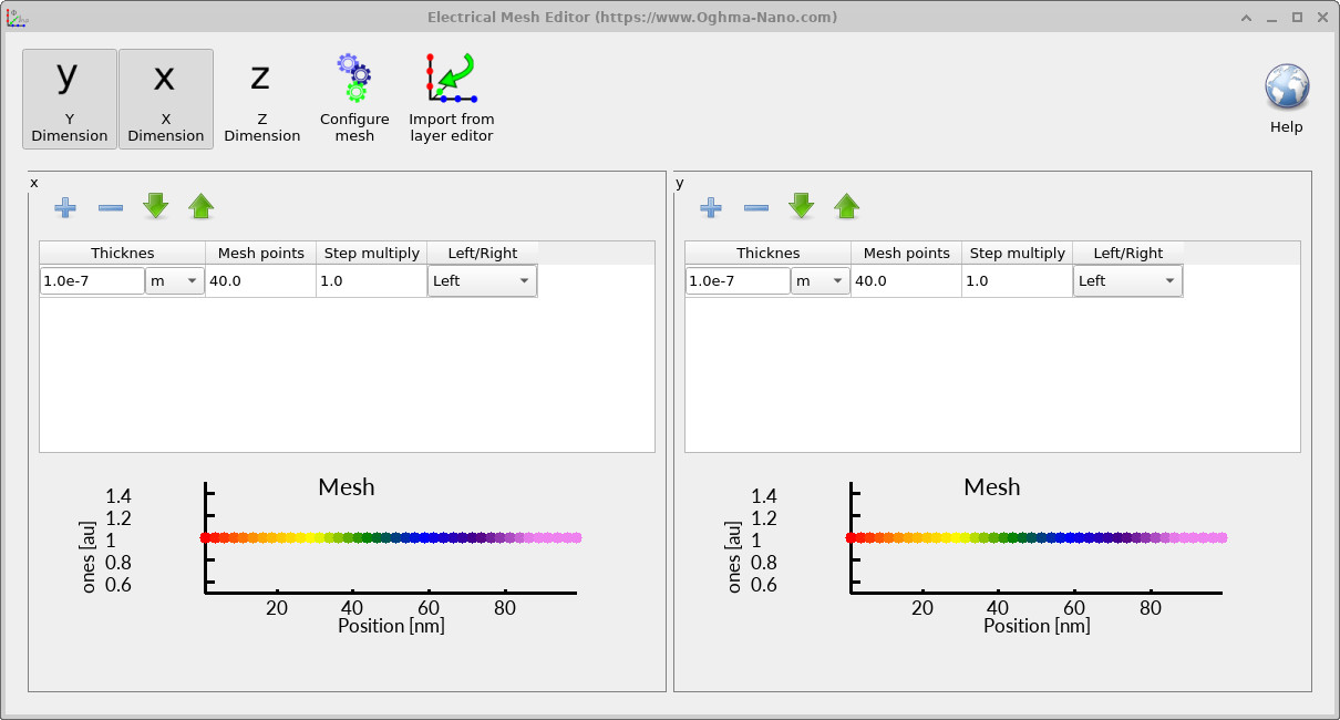
Before running the simulation, it is worth checking the electrical mesh to ensure it is sensible. In the main window, open the Electrical ribbon (Figure ??) and click Electrical mesh. This opens the mesh editor shown in ??.
In this example the mesh is 40 × 40 in the xy plane, meaning the electrical problem is solved in two dimensions. The z direction is intentionally omitted. Fully three-dimensional electrical simulations are possible in OghmaNano, but they require a true 3D morphology and come with a substantial increase in computational cost and complexity. Constructing and interpreting such models is beyond the scope of this tutorial.
Instead, this calculation should be thought of as a 2D cross-section through the device. The slice sits through the centre of the morphology and retains the full lateral BHJ microstructure within that plane. This approach captures percolation, bottlenecks, and phase connectivity while remaining fast, interpretable, and well suited to tutorial-scale exploration.
6. Running the simulation
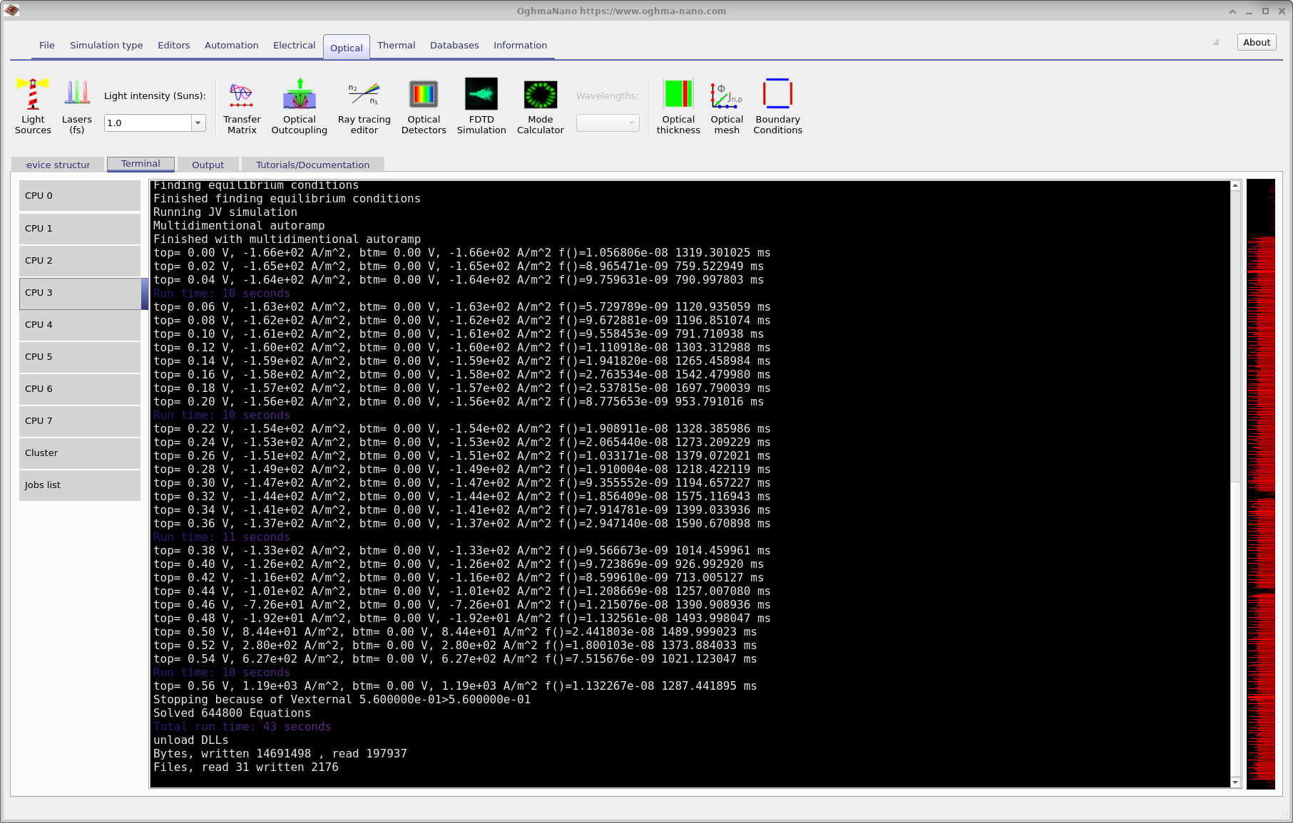
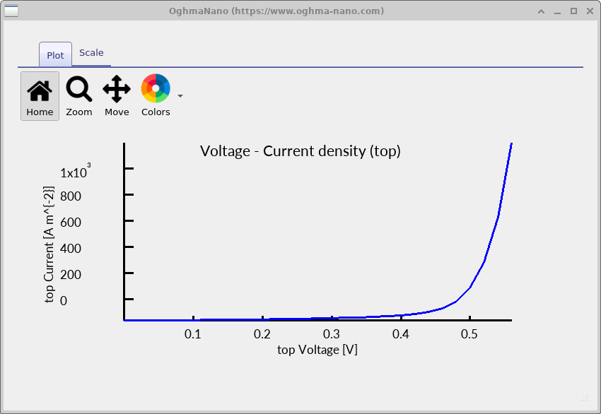
Click the blue Run simulation button in the main window to start the solver. While the run is in progress, the terminal prints the bias point and current density at each step (??). In this example the bias applied to the top contact is stepped from 0.00 V to approximately 0.54 V to generate a JV sweep. At low bias the reported current density is negative under illumination, and as the bias approaches the open-circuit regime the net current crosses through zero and changes sign, consistent with solar-cell behaviour.
When the run finishes, open the Output tab (??) to inspect the generated files. The terminal summary reports the total run time, the number of equations solved, and basic disk I/O statistics. In morphology-resolved simulations it is worth monitoring file output: writing large numbers of snapshots can dominate run time even when the solver itself is fast.
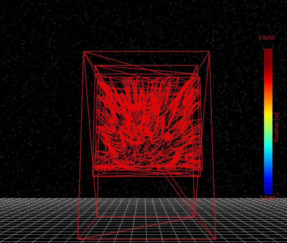
For a geometry sanity check, double-click device.csv to view the triangulated representation of the device used internally by
the solver (??). This confirms that the BHJ
morphology has been imported and discretised as expected.
To view the electrical performance, open jv_contact_0.csv or jv_contact_1.csv to plot the JV curve
(??). For this 2D simulation,
the per-contact JV outputs should be used; jv.csv can be ignored.
device.csv).
jv_contact_0.csv / jv_contact_1.csv.
7.0 Examining simulation snapshots
After the run completes, the most informative outputs are found in the
snapshots/ directory. Snapshot files are saved
internal state variables of the drift–diffusion–SRH system, written as a
function of applied bias. They expose the spatially resolved solution of the
transport equations at each voltage step, rather than post-processed summaries.
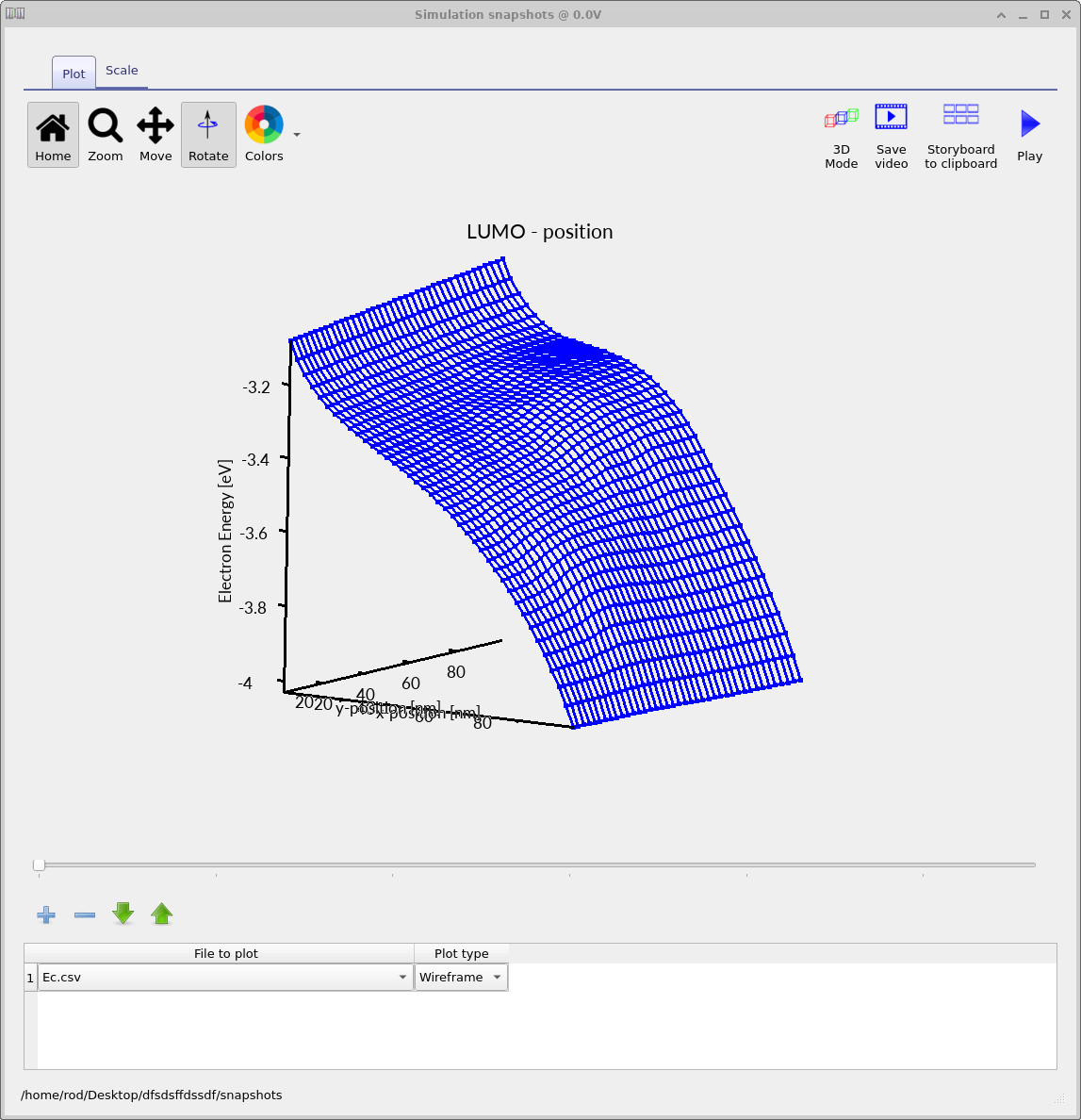
When a snapshot is opened, two controls become available: a bias
slider, which steps through the JV sweep, and a cut-through
position slider, which selects the 2D slice through the morphology.
Throughout this tutorial the electrical problem is solved on a 2D slice, and
all snapshot data correspond to that slice.
Figures
??–
??
show representative 2D snapshots at a fixed bias. These quantities should be
interpreted together. The conduction-band (LUMO) landscape,
Ec.csv (??),
defines the energetic environment for electrons. In a morphology-resolving
simulation this landscape varies laterally due to both phase-dependent
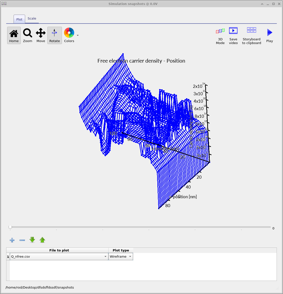
energetics and electrostatic response to local charge accumulation. The free-electron density,
Q_nfree.csv (??),
highlights regions where electrons can move efficiently through the
acceptor/matrix network. Strong spatial variations indicate percolation paths,
constrictions, and morphology-induced bottlenecks.
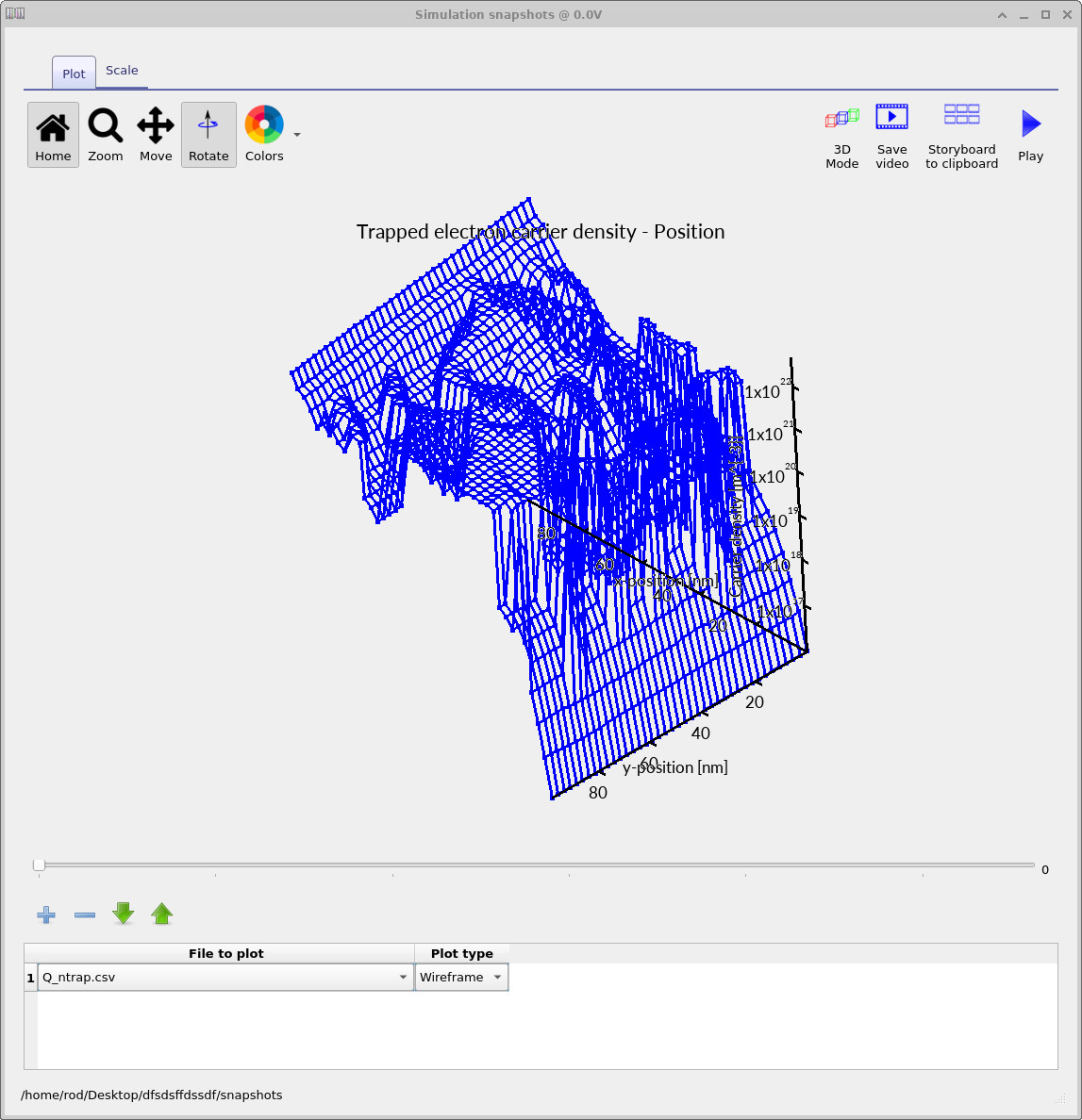
The trapped-electron density,
Q_ntrap.csv (??),
reveals where carriers accumulate in trap states. Comparing free and trapped
densities is often the fastest way to identify regions of poor extraction or
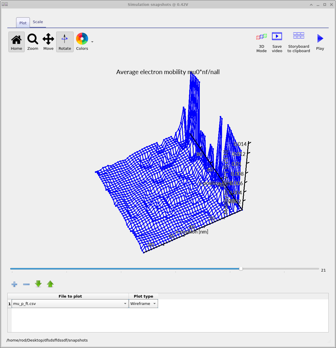
strong local trapping tied to the BHJ morphology. The mobility-related output,
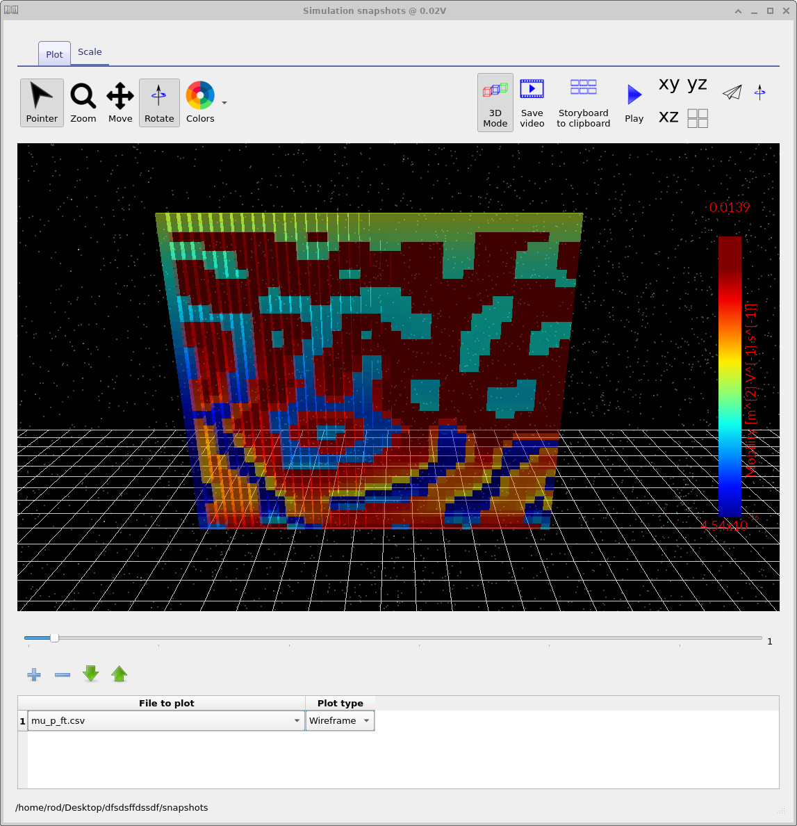
mu_p_ft.csv (??),
shows an effective mobility averaged over free and trapped carriers. Spatial
variations reflect both intrinsic phase contrast and local trapping, and often
correlate strongly with connectivity of the underlying network.
Ec.csv: conduction-band (LUMO) landscape.
Q_nfree.csv: free electron density.
Q_ntrap.csv: trapped electron density.
mu_p_ft.csv: mobility averaged over free and trapped carriers.
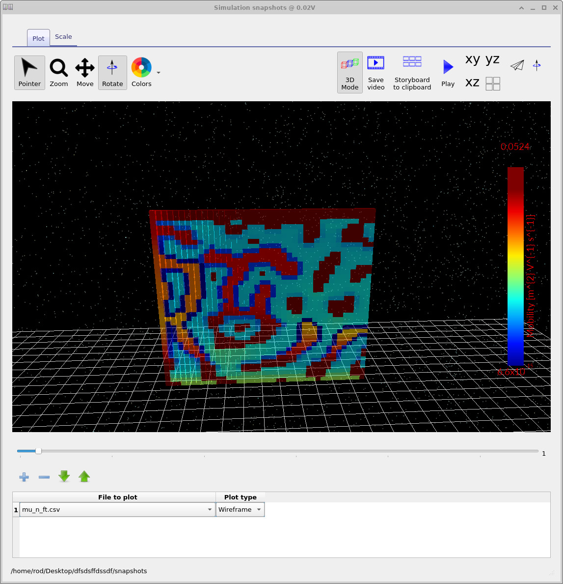
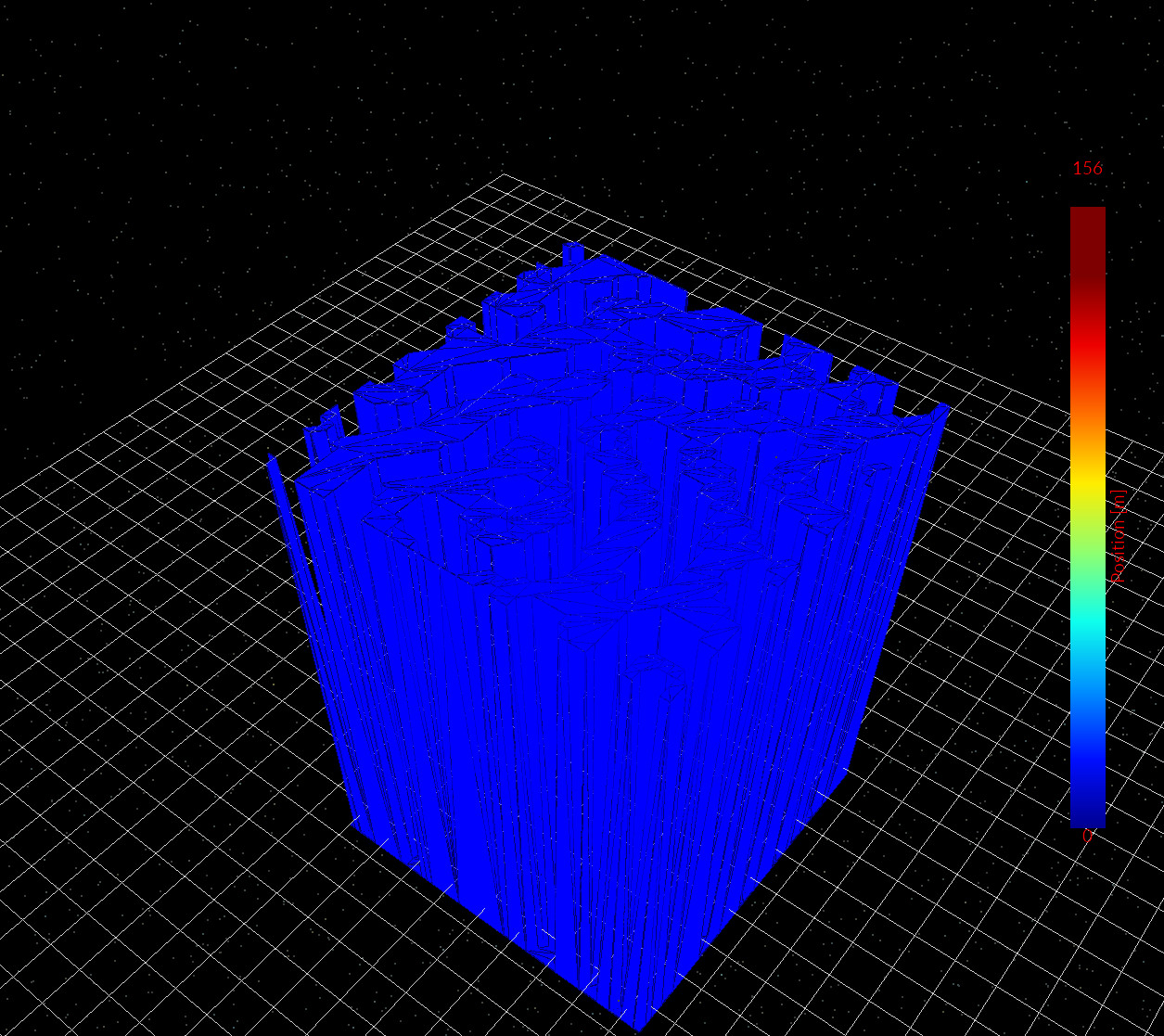
While 2D views are often the clearest way to analyse spatial variation, it is
sometimes easier to interpret the same data in real space. By enabling
3D mode in the snapshot window, the 2D slice is projected back
into the device geometry. Figures
??–
??
show examples of this projection. The averaged electron and hole mobilities
(mu_n_ft.csv, mu_p_ft.csv), the free-electron
quasi-Fermi level (Fn.csv), and the electron current density in the
transport direction (Jn.csv) are particularly useful for visualising
percolation pathways and current flow through the BHJ.
These snapshot outputs provide the main scientific value of morphology-resolving simulations: they allow device-scale observables to be directly linked to local energetics, trapping, and connectivity within the bulk heterojunction.
mu_n_ft.csv: average electron mobility (3D view).
mu_p_ft.csv: average hole mobility (3D view).
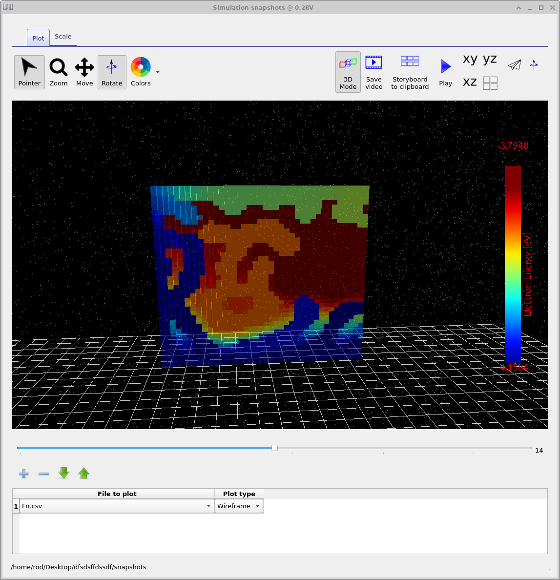
Fn.csv: free-electron quasi-Fermi level.
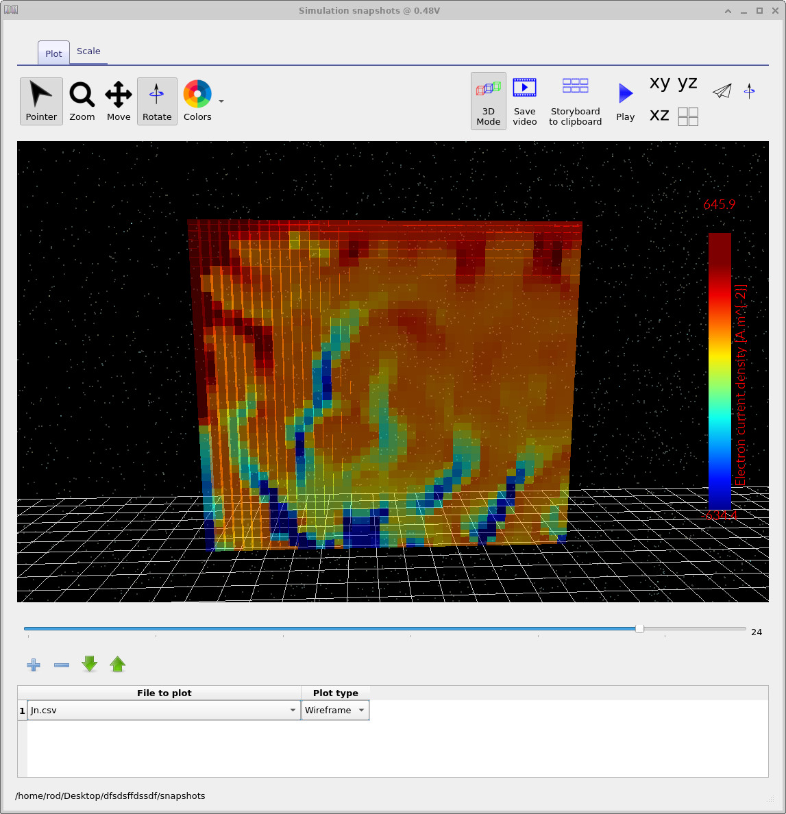
Jn.csv: electron current density (y direction).
8. Tasks to try
The fastest way to build intuition is to perturb the model and watch what changes. The tasks below are designed to be quick: swap the morphology mesh, re-run, and compare the JV curve (and, if you have time, a couple of snapshots at the same bias).
Task 1 — swap the morphology mesh
In the main device view, right-click the red BHJ object (the embedded polymer mesh) and select Mesh editor. In the editor, the current option should be Shape from database. Change the selected shape to morphology/1, morphology/2, and morphology/3 (Figures ??, ??, ??). Re-run the simulation after each change and compare the JV curve.
What you are looking for is how connectivity and bottlenecks alter extraction and recombination: some morphologies produce cleaner percolation paths (higher current), while others force carriers through narrow necks and dead-ends (more accumulation, more trapping, and typically worse JV performance).
As a deliberately "wrong but instructive" experiment, you will also find a shape called teapot in the database. Swap the BHJ mesh to teapot, re-run, and generate a JV curve for a device with a teapot-shaped inclusion. It is not a physically sensible BHJ, but it demonstrates that the workflow is genuinely geometry-driven: any closed CAD mesh can be inserted and electrically analysed.
Task 2 — change trapping strength (SRH trap bands)
In Electrical parameters, adjust the non-equilibrium SRH traps settings and re-run. Try one change at a time:
- Increase/decrease the trap density by 1-2 orders of magnitude and compare
Q_nfreevsQ_ntrap.
The point of this task is to see how dispersive/trap-limited transport competes with morphology: trapping tends to amplify "bad" regions (dead-ends, constrictions) because charge cannot empty as quickly.
Task 3 — change recombination rate constants
Still in Electrical parameters, modify recombination and re-run. Two simple perturbations:
-
Change the free-to-free recombination rate constant (
n_freetop_free) up/down by 1–2 orders of magnitude. Watch how the JV curve and the spatial distribution of charge respond. -
If your project exposes SRH capture/coupling parameters (free↔trap coupling constants), scale them up/down together and compare the
balance of
Q_nfreeandQ_ntrapat the same bias.
A useful habit for Tasks 2–3 is to keep the morphology fixed, change one knob, and then check the same two things each time:
(i) how the JV curve shifts, and (ii) whether the current pathways (e.g. Jn and quasi-Fermi level fields) become smoother
or more “fractured” by the microstructure.
📘 Return to the introduction to organic electronics for a broader overview of the topic.