1.Meshing
1. What is meshing?
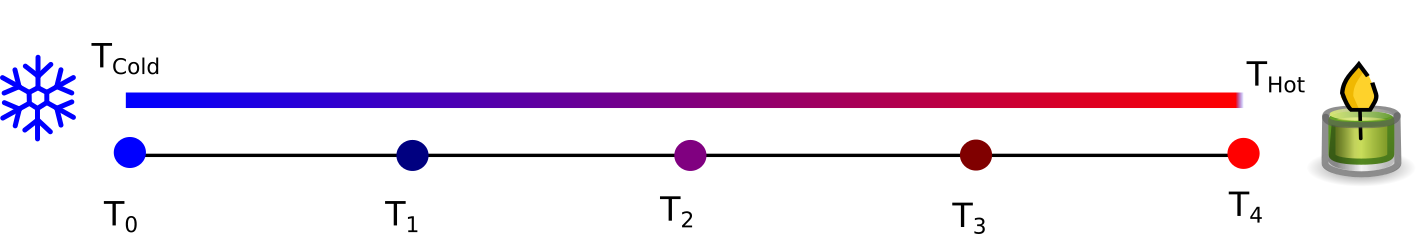
Meshing is the process of dividing a continuous physical region into a set of discrete points that can be handled by a computer. For example, imagine heat flowing along a metal bar from a candle flame at one end to a block of ice at the other. In reality, temperature varies continuously along the bar, but a simulation cannot store infinitely many values. Instead, the bar is represented by a finite number of sample points (a mesh), and calculations are performed only at those locations (see ??). By working with a mesh, we convert an otherwise continuous problem into a discrete one that can be solved using numerical methods. This principle underlies finite-difference, finite-element, and other computational approaches widely used in physics and engineering.
2. Different meshes for different problems
In OghmaNano, three core physical models are solved: the optical model (light absorption and propagation), the thermal model (heat generation and flow), and the electrical model (charge transport and recombination). Each of these processes typically occurs on very different length scales, so each requires its own mesh. For example:
- Organic solar cell: Electrically relevant effects are concentrated in the active layer (≈100 nm thick), so drift–diffusion equations only need to be solved there. However, light interacts with all layers of the device stack (≈1 µm thick), so the optical problem must be solved across the full device. In this case, the optical mesh spans the entire stack, while the electrical mesh is focused on the active layer.
- Quantum Well laser diode: The device may generate significant heat in its quantum wells (≈30 nm thick) and waveguide layers (≈1 µm thick), but this heat ultimately dissipates through a large copper heat sink that is centimeters thick. Here, electrical effects must be modeled on the nanometer-to-micrometer scale inside the device, whereas thermal effects require a mesh extending out to the centimeter scale of the heat sink.
In practice, this means different physical effects must be simulated on different length scales. Additionally, device structures often include very thin contact or interface layers just a few nanometers thick. Optically, such layers are far below the wavelength of light and can often be ignored, but electrically they are critical because they determine the current–voltage behavior of the device. To capture these effects, you would use a very fine electrical mesh in those regions, while the optical mesh can remain coarser and span over them.
OghmaNano automatically interpolates between meshes when coupling models. For example, if you define a thermal profile on the thermal mesh but the electrical solver requires local temperature values, they are transferred through interpolation. The same applies for optical quantities such as the carrier generation rate, which are interpolated from the optical mesh onto the electrical mesh as needed. As a user, you do not need to manually manage these transfers.
3. The three meshes of OghmaNano
OghmaNano provides three independent meshes - thermal, optical, and electrical - which can be defined separately depending on the problem being solved. Each mesh is accessed from its corresponding ribbon tab, as shown in Figure ??.
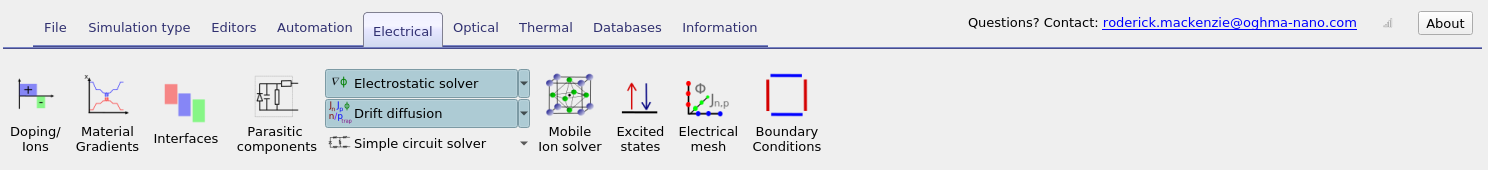
3.1 Electrical mesh
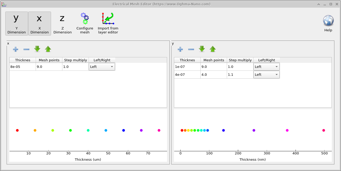
Clicking the Electrical mesh button in the Electrical ribbon opens the mesh editor window (??). At the top of this window are the X, Y, and Z buttons. These toggle which spatial dimensions are active in the simulation. For example, activating only Y enables a 1D simulation, while enabling X and Y together sets up a 2D simulation. In the example shown, both X and Y are active, so the mesh is configured for a 2D OFET simulation. The central tables function like spreadsheets and define the mesh structure for each active dimension. Their main columns are:
- Thickness: the physical thickness of each mesh region.
- Mesh points: the number of discretization points in that region.
- Step multiply: how much the grid spacing grows within the region.
For example, a value of
1.1increases each step by 10% relative to the previous one. - Left/Right: sets the side of the device from which the mesh is generated.
The resulting meshes are plotted in the graphs at the bottom of the window, giving immediate feedback on point spacing and distribution. The Import from layer editor button provides a shortcut for complex devices. It clears the Y-mesh and automatically imports all layers from the Layer Editor, assigning four mesh points per layer. This is especially useful for structures with many layers, such as laser diodes.
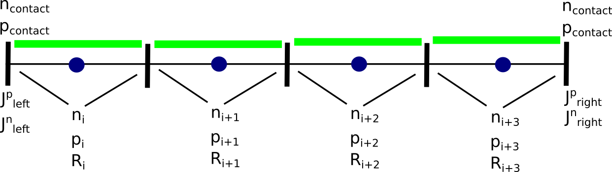
The electrical mesh in detail: ?? illustrates how the electrical mesh is constructed. The mesh does not begin exactly at the device boundary, but instead starts half a mesh spacing inside the device. This ensures that the first computational node lies within the active simulation region, allowing boundary conditions (for example, electrical contacts) to be applied at well-defined positions just outside the mesh. The same convention is applied at the far edge of the device, so the mesh extends half a step beyond the final physical point.
- It avoids numerical issues that arise when attempting to evaluate derivatives directly on boundaries.
- It places the first and last mesh points in positions that best represent the physical device interior, while still enabling external conditions to be imposed consistently.
Automatic meshing: Layer thicknesses are defined in the layer editor. After defining the physical device structure, the user should update the electrical mesh so that the mesh geometry matches the physical dimensions of the device. In practice, new users often do not realise that the electrical mesh, like any CAD representation, must be consistent with the physical object size.
To reduce setup errors, OghmaNano applies automatic meshing assumptions at runtime. The simulation assumes that the layer widths and heights specified in the layer editor are correct and attempts to map these dimensions onto the electrical mesh automatically. For example, if a device consists of a single layer and the corresponding mesh height is incorrect, the simulation will internally use the layer thickness from the layer editor when constructing the mesh.
If the number of device layers matches the number of vertical mesh layers, each mesh layer is automatically associated with the corresponding device layer thickness. These adjustments are applied internally during the simulation and do not modify the visible mesh parameters in the editor. If the number of mesh layers does not match the number of active device layers, or if the mapping is ambiguous, automatic meshing is not applied and the simulation will terminate with an error indicating that the mesh definition is inconsistent with the device structure.
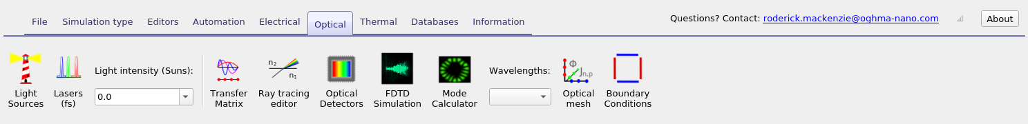
3.2 Optical mesh
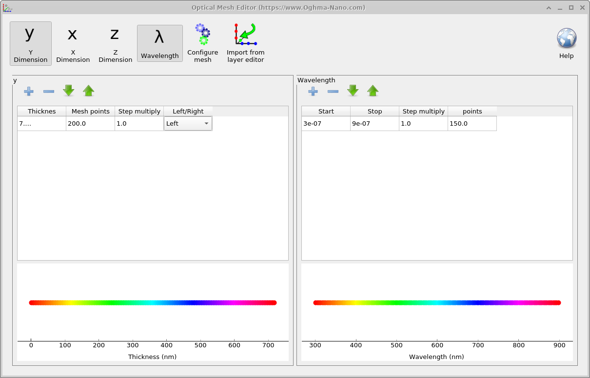
The optical mesh editor (??) is similar in layout to the electrical mesh editor but includes an additional panel for defining the wavelength mesh. At the top of the window, the X, Y, and Z buttons toggle which spatial dimensions are active, while the λ (Wavelength) button enables the spectral grid.
The left-hand panel specifies the spatial discretization in nanometers, using the same columns as the electrical mesh (Thickness, Mesh points, Step multiply, and Left/Right). The right-hand panel defines the spectral range by setting the Start and Stop wavelengths, the number of points, and the step multiplier. These wavelength points are used consistently across all optical solvers, including ray tracing, FDTD, and transfer matrix simulations.
Automatic meshing: For optical simulations, the software will attempt to automatically adjust the optical mesh so that its dimensions are consistent with the optical problem. In more complex two- or three-dimensional simulations, if the optical and electrical meshes do not match, the solver will attempt to update them automatically. If this is not possible, or if the intended mesh configuration cannot be determined unambiguously, the simulation will terminate with a clear error indicating that the mesh definitions are inconsistent.
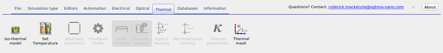
3.3 Thermal mesh
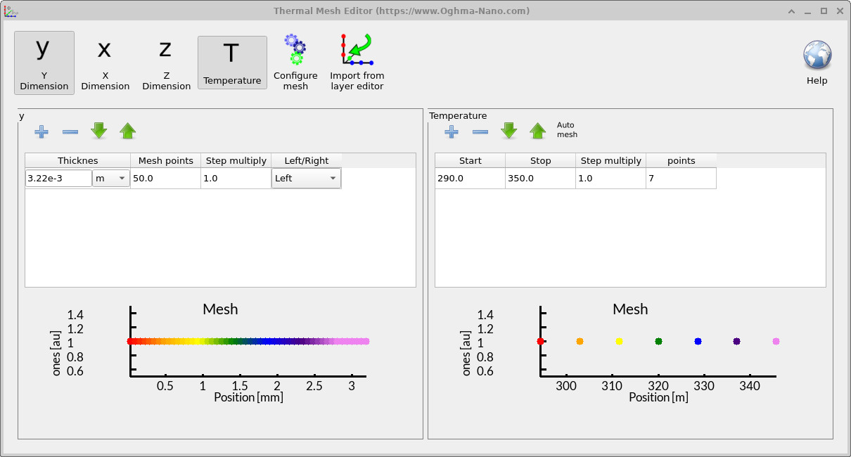
The thermal mesh editor (??) works in the same way as the electrical and optical mesh editors, with X, Y, and Z buttons to activate spatial dimensions. In addition, it includes a dedicated T (Temperature) mesh.
The temperature mesh is used whenever simulations need to account for temperature dependence, for example when enabling self-heating or when evaluating electrical properties across a temperature range. Before the simulation runs, OghmaNano pre-calculates and tabulates quantities such as carrier densities versus Fermi level and temperature, or Fermi–Dirac integrals. These tables allow the solver to quickly look up values during the run, rather than computing them repeatedly.
In most cases the thermal mesh is handled automatically, but advanced users may adjust the range and resolution to ensure sufficient accuracy for strongly temperature-dependent problems.
4. When do I need to worry about meshing in OghmaNano?
Electrical mesh: The Layer Editor splits a device into layers of different materials (see Section 3.1.3). Layers marked as active are those over which the electrical model is applied. For these layers, a finite-difference mesh must be defined. The mesh length must match the active layer length exactly-otherwise an error will occur. OghmaNano will usually generate a suitable mesh automatically, so for most simple devices this does not require manual intervention. However, when multiple active layers are present, or when the number of mesh points needs to be reduced to speed up a simulation (or increased for higher accuracy), the electrical mesh may need to be configured manually.
Optical mesh: The optical mesh controls both spatial and wavelength sampling. It may need to be adjusted to change the simulated wavelength range or to refine how light interacts with different layers of the device. Increasing the number of mesh points improves optical accuracy but increases simulation time.
Thermal mesh: The thermal mesh is only relevant when self-heating is enabled. In this case, it provides the resolution required to model temperature variations across the device and the coupling of thermal effects to traps and recombination processes. Otherwise, it is handled automatically by OghmaNano.
5. Meshing tips
Should I be simulating in 1D, 2D, or 3D?
Choosing the correct dimensionality is one of the most important decisions when setting up a simulation. Always use the minimum number of dimensions required to capture the physics of interest-this saves time and computational resources.
- Solar cells: Typically require only 1D meshes, since variations are primarily along the vertical (thickness) direction.
- Optical filters: Also usually 1D, as the key optical interference occurs in the stack direction.
- OFETs: Require 2D, since both vertical current flow through the semiconductor and lateral current between source and drain must be resolved.
Speed vs. accuracy
It is tempting to assume that adding more mesh points always improves accuracy. In practice, more points can help-up to a point- but they can also make a simulation less accurate or less stable. The limiting factor is often not raw computing power, but numerical conditioning: many device simulations contain quantities that differ by many orders of magnitude (for example, very small densities or recombination rates alongside very large fields, currents, or dopings). Because computers use finite-precision arithmetic, operations involving extremely large and extremely small numbers can lose significant digits. This loss of precision can dominate the error budget and can trigger spurious oscillations, noisy currents, or poor convergence.
Increasing the mesh density can make this problem worse, not better. A finer mesh often introduces steeper local gradients, larger derivative terms, and stronger coupling between neighbouring nodes, which can increase the spread between the smallest and largest numbers in the linear system that must be solved. The result can be a more ill-conditioned problem, where the solver struggles to distinguish real physics from numerical noise. In such cases, a slightly coarser mesh can produce smoother fields, better conditioning, and therefore more reliable results-even though it contains fewer points.
A good workflow is to begin with a coarse mesh to validate the setup and confirm that the qualitative behaviour is correct, then refine only as much as necessary. Mesh refinement should be driven by evidence: if key outputs (e.g. JV curves, carrier profiles, optical generation) stop changing meaningfully when additional points are added, further refinement is unlikely to improve accuracy.
When setting up a device in OghmaNano, keep the following guidelines in mind:
- Use the minimum dimensionality: 1D whenever possible; move to 2D/3D only when the physics requires it.
- Minimise mesh points where possible: Aim for the smallest number of points that still captures the essential physics. This improves speed and can improve numerical robustness.
- More points ≠ always better: If increasing mesh density leads to noisy currents, convergence problems, or unstable profiles, try reducing the number of points and/or refining only in the regions that matter.
- Use coarse meshes for exploration: When testing fits or investigating general device behaviour, reduce mesh density to get rapid feedback, then refine selectively for accuracy.
- Refine with a purpose: Add points where gradients are real (interfaces, depletion regions, thin layers), not everywhere. Uniform refinement is often the least efficient option.