

Built-in potential in drift-diffusion simulations
The built-in potential, \(V_{bi}\), is the internal electrostatic potential that forms when two contacts or semiconductor regions with different Fermi-level positions are brought into electrical contact. In drift-diffusion simulations, the built-in potential determines the equilibrium band bending, sets the initial electric field, and defines the starting point for solving Poisson’s equation and the carrier continuity equations.
Figure ?? shows the formation of a built-in potential from the alignment of Fermi levels. In panel (a), the two materials are isolated. The material on the left contains a high density of holes, while the material on the right contains a high density of electrons. Because the two materials are not yet in electrical contact, their electrochemical potentials are independent and their Fermi levels do not need to be aligned.
When the two materials are brought into contact, as shown schematically in panel (b), carriers can redistribute between them. Electrons move from the material with the higher electron chemical potential towards the material with the lower electron chemical potential, while holes redistribute in the opposite sense. This charge transfer cannot continue indefinitely: it leaves behind ionised charge and produces an internal electric field. At thermodynamic equilibrium, the net driving force for carrier motion vanishes and the Fermi level becomes spatially constant across the combined structure.
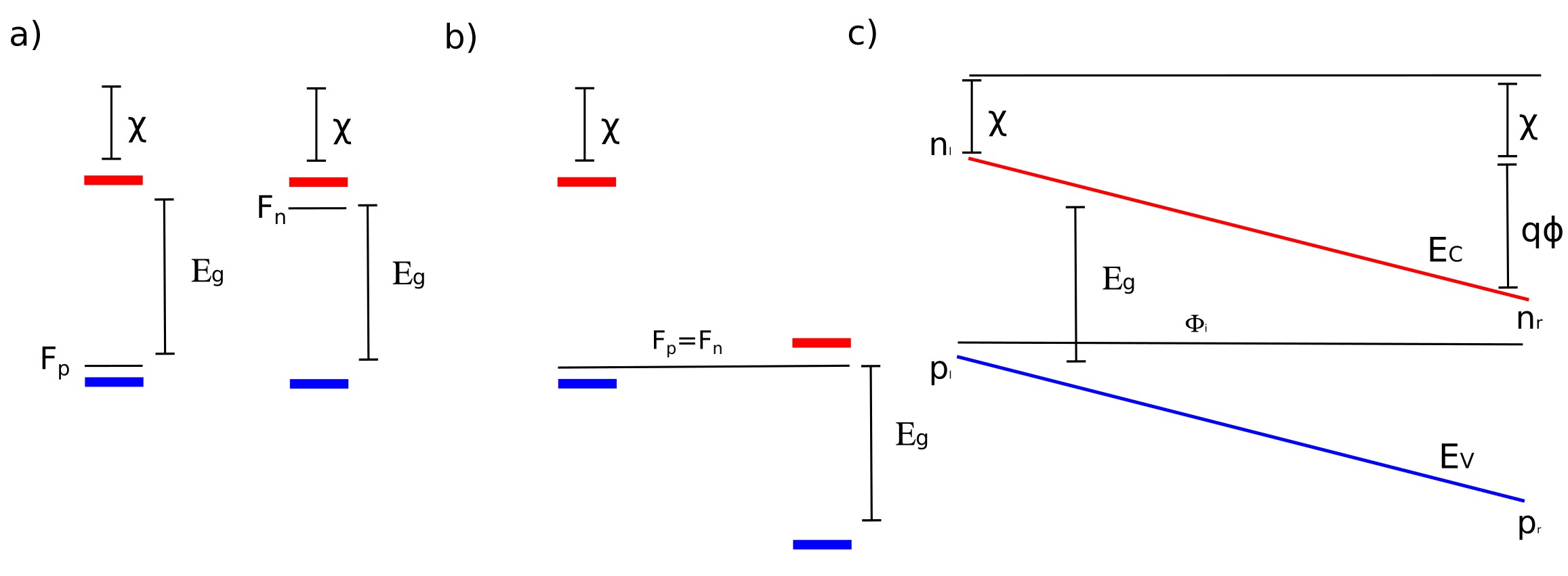
Panel (c) shows the corresponding band diagram after equilibrium has been reached. The conduction-band edge, \(E_C\), and valence-band edge, \(E_V\), bend across the junction because the electrostatic potential varies with position. The built-in potential, \(\Phi_i\), is the electrostatic potential difference required to align the Fermi levels of the two originally separate materials. Equivalently, it is the potential drop associated with the internal electric field formed by the redistribution of charge.
This is the same physical mechanism that produces the built-in voltage in a semiconductor junction or between two asymmetric contacts in a device. Before contact, the two sides can have different work functions, carrier densities, or Fermi-level positions. After contact, equilibrium requires a single Fermi level, and the difference is accommodated by band bending and an internal electrostatic potential. In drift-diffusion simulations, this built-in potential enters through the electrostatic potential and therefore modifies the local carrier densities, current flow, and injection barriers at the contacts.
2. Calculating the built-in potential
The derivation below gives the built-in potential equation used in the simulation from the contact electron and hole densities, rather than from dopant concentrations. This form is useful for organic semiconductors, thin-film solar cells, OLEDs and other devices where boundary carrier densities are specified directly.
In drift-diffusion simulations, the first step is to determine the built-in potential of the device structure. This arises from the requirement that the Fermi level must be spatially constant at equilibrium (see ??). If the two contacts impose different carrier densities, this condition can only be satisfied through the formation of an internal electrostatic potential. Here the band edges are written as \(E_C\) and \(E_V\); in organic semiconductors these are equivalently represented by the LUMO and HOMO levels, \(E_{LUMO}\) and \(E_{HOMO}\).
In the equations below, \(\phi\) denotes the electrostatic potential shift and \(V_{bi}\) denotes the total built-in potential across the device.
To evaluate the built-in potential, the following quantities are required:
- The carrier concentrations at the contacts, \(n\) and \(p\).
- The effective densities of states, \(N_c\) and \(N_v\).
- The effective band gap, \(E_g\).
The left-hand contact is taken as the reference with an electrostatic potential of \(0\) V. The corresponding band edges are therefore
\[ E_C = -\chi \quad,\quad E_V = -\chi - E_g \]
Assuming Maxwell–Boltzmann statistics, the carrier concentrations on the left-hand side are
\[ n_l = N_c \exp\!\left(\frac{F - E_C}{kT}\right) \quad,\quad p_l = N_v \exp\!\left(\frac{E_V - F}{kT}\right) \]
At equilibrium the Fermi level \(F\) is constant throughout the device. If the right-hand contact imposes different carrier densities, this condition is satisfied by shifting the band edges by an electrostatic potential \(\phi\):
\[ E_C = -\chi - q\phi \quad,\quad E_V = -\chi - E_g - q\phi \]
The carrier concentrations on the right-hand side then become
\[ n_r = N_c \exp\!\left(\frac{F - E_C}{kT}\right) \quad,\quad p_r = N_v \exp\!\left(\frac{E_V - F}{kT}\right) \]
The built-in potential in the drift-diffusion model is therefore the electrostatic shift required to reconcile the imposed boundary carrier densities with a single, spatially constant Fermi level. The explicit expression for \(\phi\) follows directly from this condition.
2.1 Built-in potential equation from carrier densities
Rearranging the electron density expression,
\[ n = N_c \exp\!\left(\frac{F-E_C}{kT}\right) \quad \Rightarrow \quad F - E_C = kT \ln\!\left(\frac{n}{N_c}\right) \]
Evaluating this at each contact (before electrostatic alignment) gives
\[ F_l = -\chi + kT \ln\!\left(\frac{n_l}{N_c}\right) \quad,\quad F_r = -\chi + kT \ln\!\left(\frac{n_r}{N_c}\right) \]
At equilibrium the Fermi levels must coincide, so their initial difference is converted into an electrostatic potential difference:
\[ qV_{bi} = F_r - F_l \]
Substituting gives
\[ qV_{bi} = kT \ln\!\left(\frac{n_r}{N_c}\right) - kT \ln\!\left(\frac{n_l}{N_c}\right) \]
and hence
\[ V_{bi} = \frac{kT}{q} \ln\!\left(\frac{n_r}{n_l}\right) \]
Equivalently, using the hole density,
\[ V_{bi} = \frac{kT}{q} \ln\!\left(\frac{p_l}{p_r}\right) \]
This form of the built-in potential equation is the one used internally in drift-diffusion simulations, where carrier densities at the contacts are specified directly.
This procedure determines both the built-in potential and the associated minority carrier densities at the contacts. Infinite recombination velocity is assumed, such that the carrier densities are fixed by local equilibrium. Finite recombination velocities introduce additional parameters and are typically not required to reproduce experimental device characteristics.
Why is the built-in potential important?
The built-in potential sets the internal electric field of the device and therefore controls charge separation, injection, and extraction. Errors in its calculation propagate directly into predicted current–voltage characteristics and recombination profiles.
With the built-in potential known, we can make an initial estimate of the potential profile across the device using a linear approximation. From this, approximate charge carrier densities are obtained. These serve as the starting values for the main Newton solver, which then computes the self-consistent potential and carrier distributions. The Newton solver is described in the following section.