GaAs PN Junction Diode Simulation: Drift–Diffusion, I–V Curves & Recombination
1. Introduction
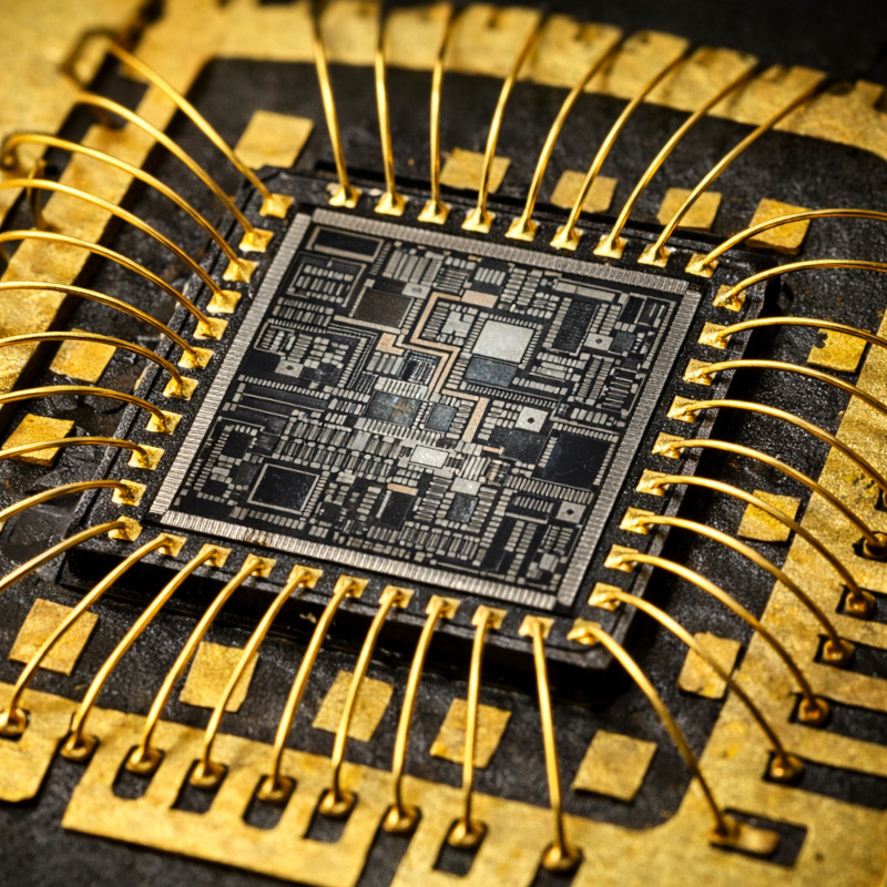
The gallium arsenide (GaAs) PN junction diode is a fundamental III–V semiconductor device. It is widely integrated into GaAs RF and microwave integrated circuits, where compact PN junctions support rectification, biasing, protection, and switching functions within the RF front-end. A representative application context is shown in ??, illustrating the kind of GaAs chip-scale platform used in modern high-frequency electronics.
Gallium arsenide is well suited to these applications because its high electron mobility enables fast carrier transport and low resistive loss, supporting efficient operation at GHz and millimetre-wave frequencies used in 5G systems. In practice, short PN junctions like the one modelled here appear throughout RF designs as bias elements, clamps, ESD and protection diodes, and switching structures. The layer stack in ?? reflects the compact vertical geometry used on-chip: thin, heavily doped contact regions paired with a short active junction.
Although the device simulated in this tutorial is simple, it should be understood as a primitive building block. The same junction electrostatics governs diode-connected structures, isolation regions, and injection layers inside GaAs technologies used for high-speed electronics and optoelectronics. The layered doping structure used here is illustrated schematically in ??.
In this tutorial you will simulate a GaAs PN junction diode in one dimension using OghmaNano’s coupled drift–diffusion + Poisson solver. Rather than relying solely on the ideal Shockley equation, this approach resolves the built-in electric field, the depletion region, and the spatial distributions of carrier densities and currents.
2. Making a New Simulation
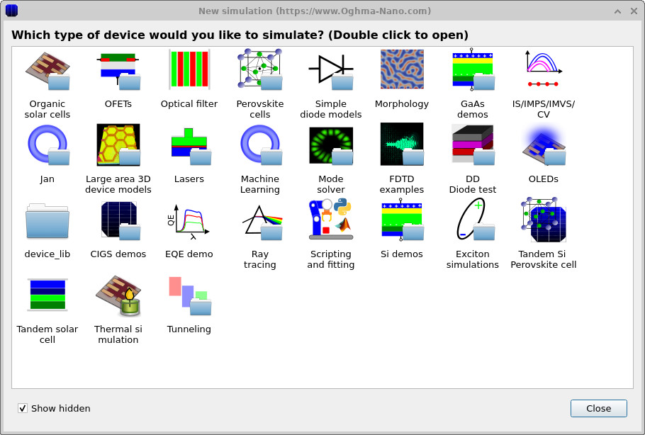
To begin, create a new simulation from the main OghmaNano window. Click on the New simulation button in the toolbar. This opens the simulation-type selection dialog (see ??).
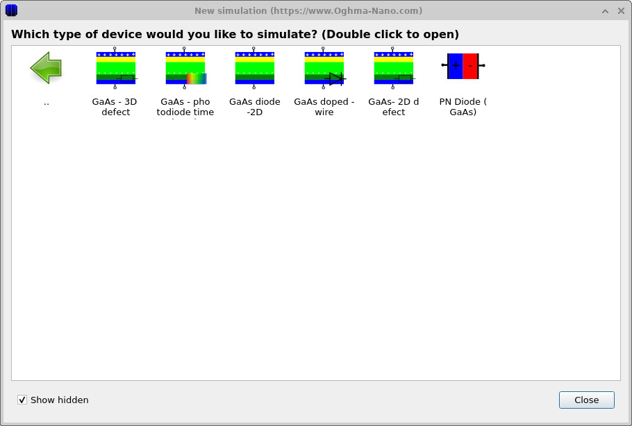
In the simulation-type dialog, double-click on GaAs demos, then select the GaAs junction/diode example (see ??). OghmaNano will load a predefined GaAs junction structure which we will treat as a PN diode.
The loaded device structure is shown in the main simulation window (see ??). Although the electrical problem solved in this tutorial is one-dimensional, the 3D view provides a clear visualisation of the vertical layer stack and the regions that participate in carrier transport and recombination.
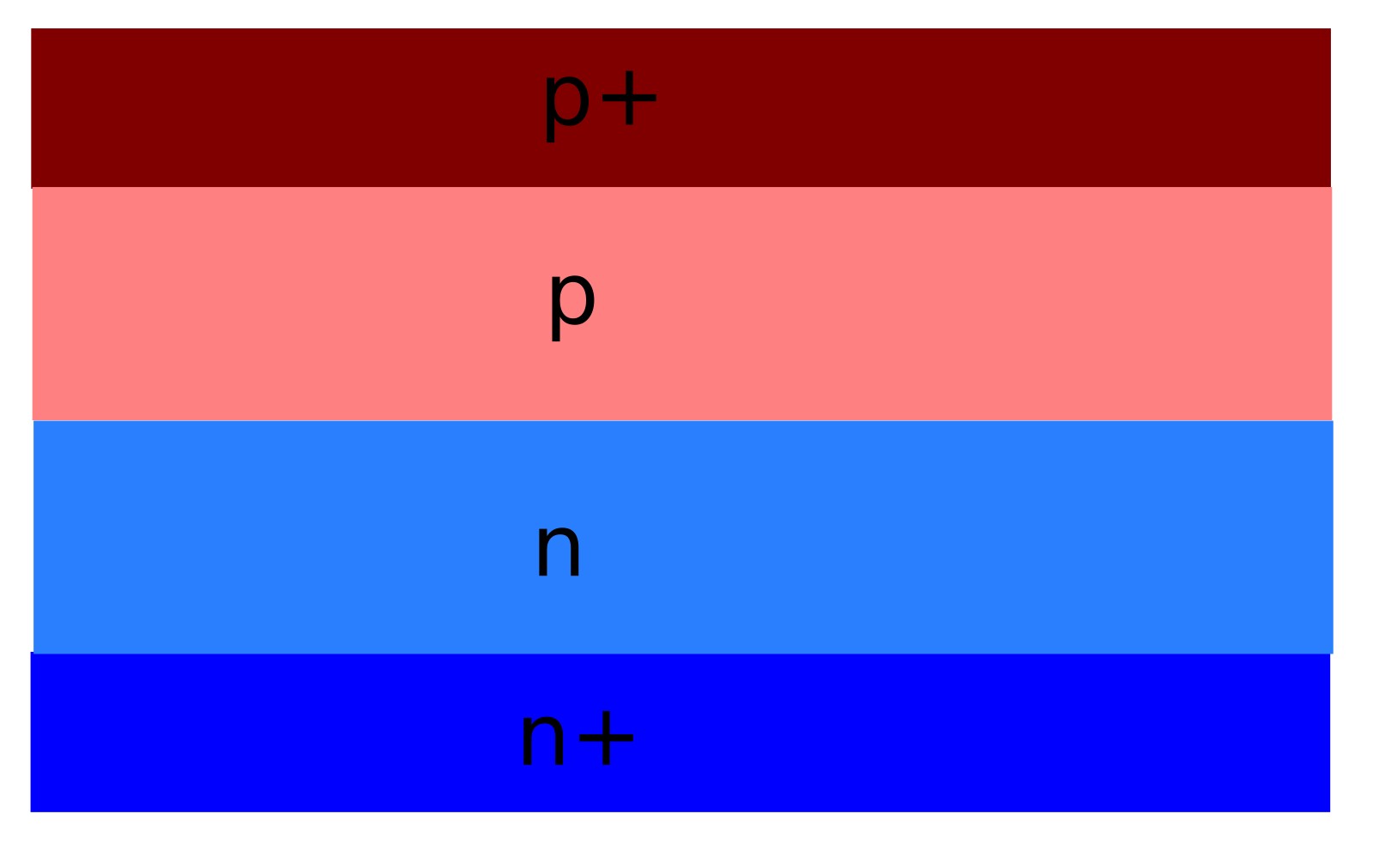
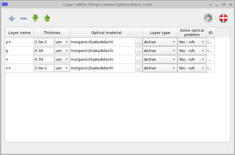
The diode is implemented as a sequence of vertically stacked GaAs layers, consisting of a heavily doped p+ region, a more lightly doped p region, a lightly doped n region, and a heavily doped n+ region. This structure is listed explicitly in the Layer editor (see ??), where each layer is assigned a thickness, material, and electrical role.
The central p and n layers form the active PN junction. At equilibrium, a depletion region develops across this interface, giving rise to the built-in electric field that controls carrier separation and transport. The thin, heavily doped p+ and n+ layers act as low-resistance contact regions, ensuring that the applied bias primarily drops across the junction rather than at the contacts.
In the sections that follow, this structure will be treated as a one-dimensional device: all variations are resolved along the growth direction, while lateral variations are neglected. Despite this simplification, the model captures the essential electrostatics, carrier transport, and recombination physics that govern the dark I–V behaviour of GaAs PN junction diodes used within practical optoelectronic and high-speed electronic device stacks.

3. Examining the doping profile
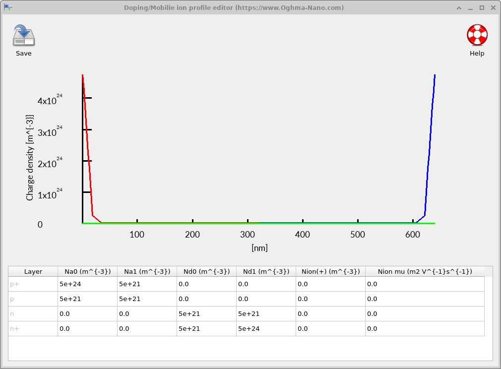
The doping profile defines the GaAs PN junction and therefore sets the fundamental electrostatics of the diode. It determines the junction position, the built-in potential, the depletion width, and the internal electric field that develops in equilibrium and under bias.
To view the doping configuration, open the Doping / Ions editor from the Electrical ribbon (see ??). The editor displays the spatial distribution of ionised donors and acceptors as a function of depth (see ??).
In this tutorial, the diode is constructed using a conventional p+/p/n/n+ GaAs doping profile. The central p and n regions are moderately doped and form the active PN junction, where the depletion region and built-in electric field develop.
The thin, heavily doped p+ and n+ layers act as low-resistance contact regions. Their role is to provide good electrical injection and extraction of carriers, while ensuring that most of the applied voltage drops across the junction itself rather than at the contacts.
For the purposes of this tutorial, the key check is simply that the device contains one predominantly acceptor-doped region and one predominantly donor-doped region, with a clear transition between them. The exact numerical values of the doping densities primarily affect the depletion width and built-in field strength, which will be explored indirectly through the diode’s dark I–V characteristics in later sections.
4. Examining electrical parameters and recombination mechanisms
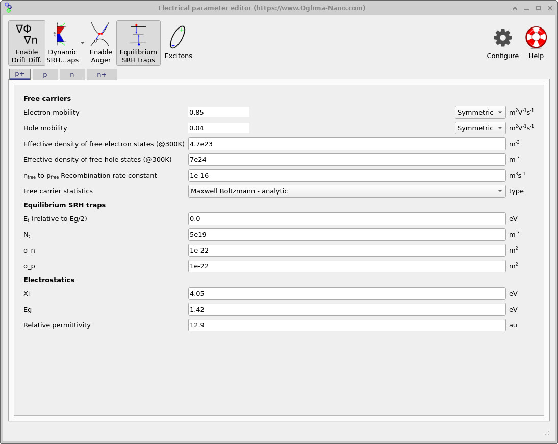
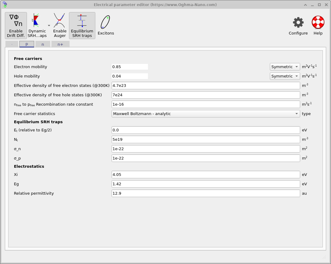
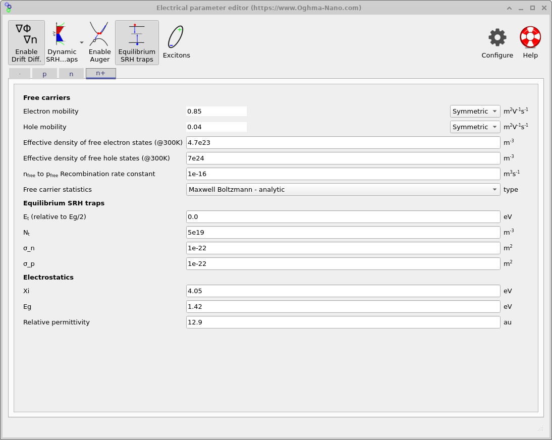
Electrical material parameters are defined on a per-region basis and control carrier transport, recombination, and electrostatics throughout the diode. Open the electrical parameter editor from the main window via Device structure → Electrical parameters. Each layer in the device stack has its own parameter tab. In this tutorial we use the same GaAs material model in all four regions, but we interpret them differently: p+ and n+ act as low-resistance contact regions, while p and n form the active PN junction.
Figures ??– ?? show the electrical parameter editor for each region (p+, p, n, n+). For GaAs, the most immediately striking parameters are the carrier mobilities: the electron mobility is high compared with silicon, while the hole mobility is more modest. This asymmetry is a defining feature of GaAs and underpins its widespread use in high-frequency electronics.
Because carrier transport in GaAs is typically fast, especially for electrons, the dark I–V behaviour of a GaAs PN junction is often not limited by bulk transport. Instead, the balance between injection, electrostatics, and recombination determines the device response. The parameters shown in the editor therefore primarily control how efficiently injected carriers are removed by recombination processes once the junction barrier is reduced.
The effective densities of states shown in the editor (e.g. ??) set the carrier statistics and equilibrium carrier concentrations for GaAs. These values differ from silicon because of GaAs’s different band structure and effective masses, and they directly influence both carrier injection levels and recombination rates through the electron and hole densities \(n\) and \(p\).

Free-to-free (radiative) recombination
Because GaAs is a direct-bandgap semiconductor, recombination between free electrons and free holes can occur efficiently via radiative transitions. In high-quality GaAs, this free-to-free recombination channel is often the dominant loss mechanism in the active junction under forward bias. In OghmaNano, this process is controlled by the free-electron–to–free-hole recombination rate constant visible in the electrical parameter editor (see, for example, ??).
The corresponding recombination rate has the form
\[ R_{\mathrm{rad}} = B \left( np - n_i^2 \right), \]where \(B\) is the free-to-free (radiative) recombination coefficient. In GaAs, this term can dominate the recombination balance once carriers are injected into the junction, particularly when defect densities are low. As a result, the dark I–V characteristic of a high-quality GaAs diode often reflects radiative recombination physics rather than defect-limited behaviour.
Shockley–Read–Hall (SRH) recombination
Shockley–Read–Hall (SRH) recombination captures defect-mediated recombination through electronic states in the bandgap. In OghmaNano this is controlled using the equilibrium SRH trap parameters shown in the editor (see ??): a trap energy \(E_t\) (relative to midgap), a trap density \(N_t\), and electron and hole capture cross-sections \(\sigma_n\) and \(\sigma_p\).
In GaAs, SRH recombination does not usually represent the intrinsic recombination limit of the material. Instead, it provides a measure of material quality and defect density. In high-quality epitaxial GaAs, SRH recombination is weak and radiative recombination dominates; in lower-quality material or near interfaces and processing damage, SRH recombination can become significant.
The SRH lifetimes are defined by
\[ \tau_n = \frac{1}{\sigma_n v_{\mathrm{th}} N_t}, \qquad \tau_p = \frac{1}{\sigma_p v_{\mathrm{th}} N_t}, \]and the resulting recombination rate is
\[ R_{\mathrm{SRH}} = \frac{np - n_i^2} {\tau_p (n + n_1) + \tau_n (p + p_1)} . \]In this tutorial, SRH recombination is retained deliberately. It allows you to explore how increasing defect density or reducing carrier lifetime shifts the diode from radiative-dominated behaviour toward recombination-limited operation, which is particularly relevant for understanding real devices where processing and interfaces play a critical role.
Electrostatics and band parameters
Finally, the band-structure and electrostatic parameters used to define GaAs are visible in each region tab (e.g. ??): the electron affinity, the bandgap (\(E_g \approx 1.42\,\mathrm{eV}\) at room temperature), and the relative permittivity (\(\varepsilon_r \approx 12.9\)). These parameters set the built-in potential of the PN junction and determine the voltage scale over which significant carrier injection occurs.
For GaAs, the combination of a direct bandgap and high carrier mobility means that once the junction barrier is reduced, carriers are injected efficiently and recombination physics becomes the dominant factor shaping the dark I–V curve. Understanding how these electrical parameters work together is therefore essential for interpreting both the simulation results and real GaAs device behaviour.
5. Running the simulation, dark I–V curves, and extracting parameters
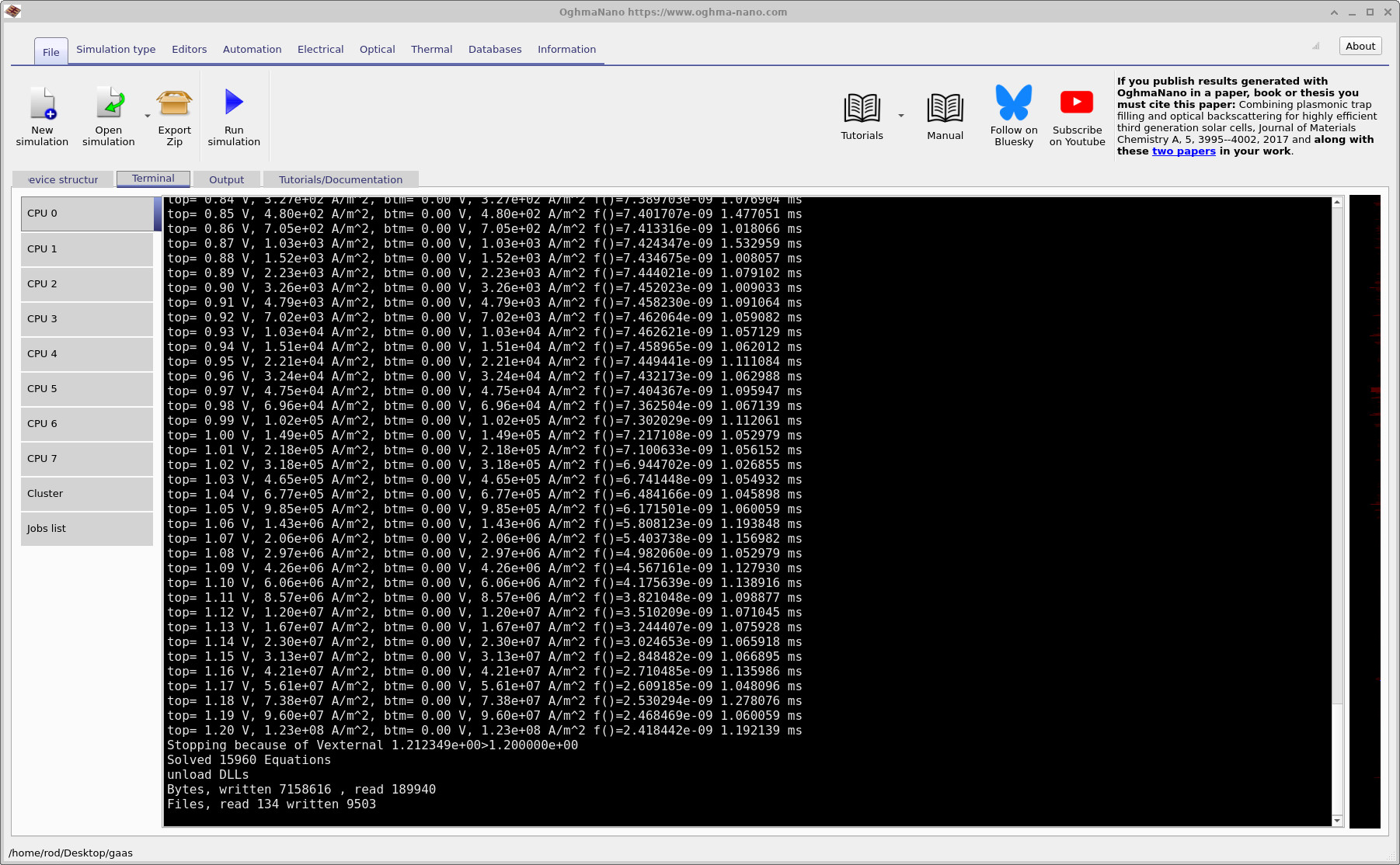
Once the device structure, doping profile, and electrical parameters are defined, the diode simulation can be run directly from the main window. Click Run simulation to start the solver. During execution, convergence information for each bias point is written to the terminal, allowing you to monitor solver stability and progress (see ??).
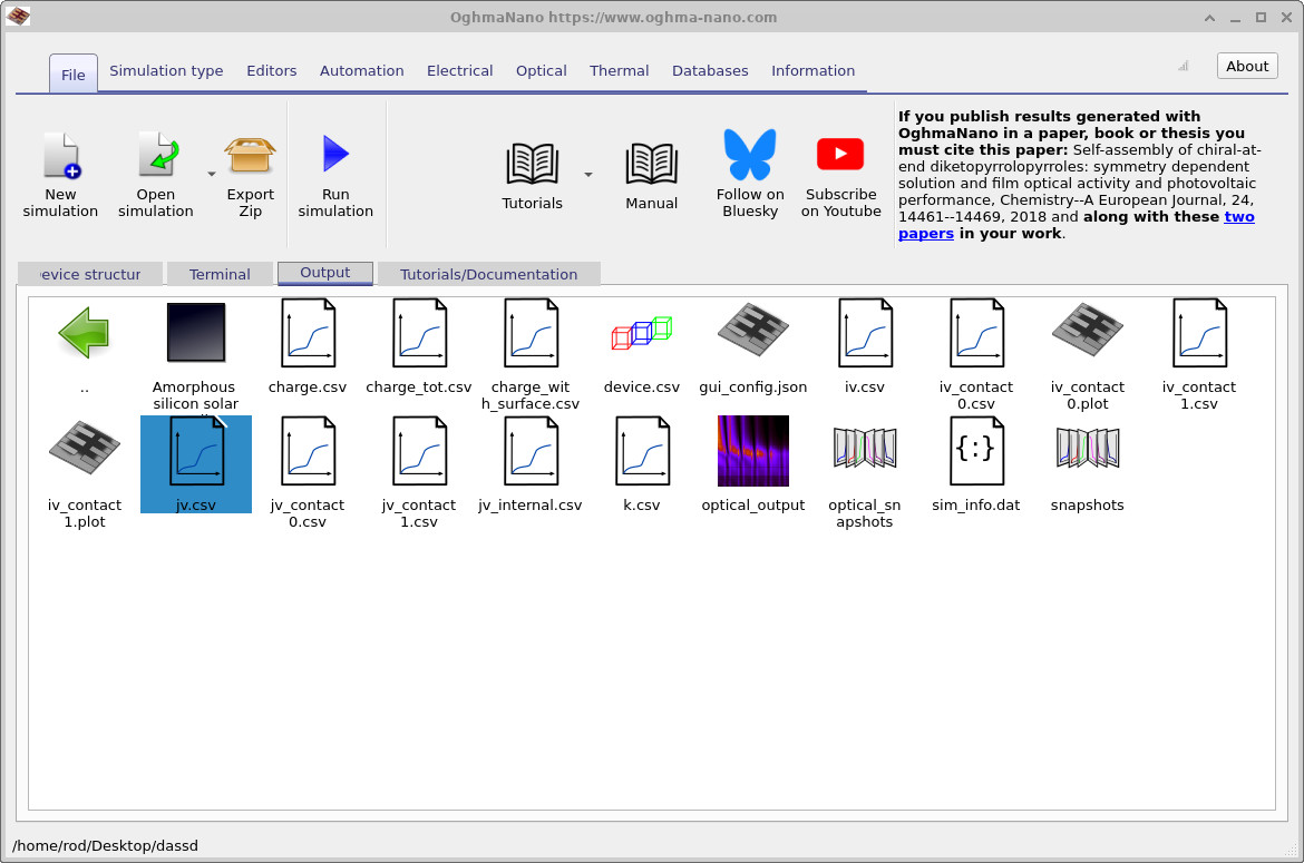
jv.csv is the primary result of interest.
To inspect the diode characteristic, open the Output tab and double-click
jv.csv
(see ??).
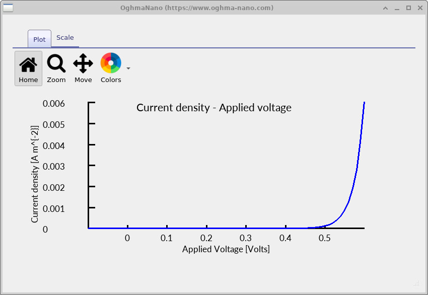
For a correctly configured GaAs diode, the I–V curve should be smooth and monotonic.
In reverse bias, the current remains small and weakly voltage-dependent,
reflecting recombination-limited saturation.
In forward bias, the current increases rapidly with applied voltage,
corresponding to carrier injection across the PN junction.
The shape of the forward-bias region contains useful physical information. On a semi-logarithmic plot, the slope of the exponential region can be used to extract an ideality factor, indicating whether the current is dominated by diffusion-limited transport (\(n \approx 1\)) or recombination-limited processes (\(n \approx 2\)). The extrapolated intercept of this region provides an estimate of the reverse saturation current, which is directly linked to the SRH and Auger recombination parameters discussed in Section 4. In GaAs, the direct bandgap and typically high mobilities mean that injection can be very efficient, so recombination settings often have a particularly clear signature in the forward-bias slope and intercept.
As a practical rule, always inspect the I–V curve before interpreting any derived quantities. Discontinuities, unexpected sign conventions, or non-physical jumps in current usually indicate issues with boundary conditions, bias stepping, recombination settings, or solver convergence. For a simple GaAs PN diode such as this, the dark I–V curve should be physically intuitive and easy to interpret.
6. Examining simulation snapshots: bands, recombination, and current flow
During an I–V sweep, OghmaNano stores the internal solution of the drift–diffusion equations at each bias point in the snapshots directory. These files expose what the solver is predicting inside the diode: band bending, quasi-Fermi level splitting, recombination activity, and current transport. Examining these quantities is essential for understanding why a particular I–V characteristic emerges.
In this section we inspect three representative bias points: a near-equilibrium reverse bias (−0.1 V), a moderate forward bias near turn-on (≈0.45 V), and a high forward bias (0.8 V). Together, these snapshots illustrate the transition from equilibrium, through injection-limited transport, to high-injection operation. For GaAs, the same qualitative transition holds, while the dominant recombination channel in the active region is typically free-to-free (radiative) rather than defect-limited SRH.
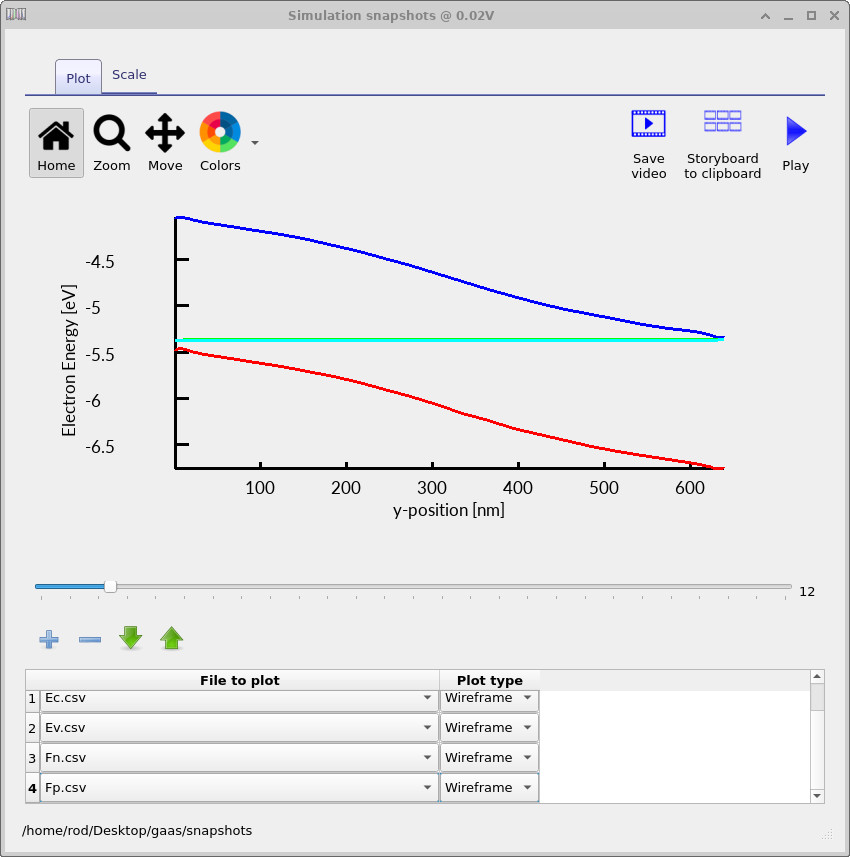
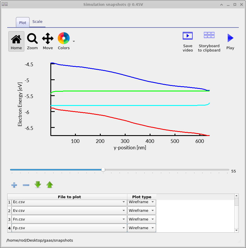
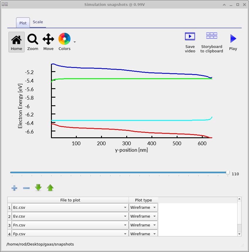
6.1 Band edges and quasi-Fermi levels
To reproduce the band diagrams, open the snapshot viewer and add the files
Ec.csv, Ev.csv, Fn.csv, and Fp.csv.
These correspond to the conduction band edge, valence band edge,
electron quasi-Fermi level, and hole quasi-Fermi level respectively.
At −0.1 V (Figure ??), the diode is close to equilibrium. The band bending reflects the built-in potential imposed by the doping profile, and the quasi-Fermi levels are nearly flat and coincident, indicating negligible net current flow. The depletion region is clearly visible as the region of strong band curvature at the junction. At ≈0.45 V (Figure ??), forward bias reduces the junction barrier. The electron and hole quasi-Fermi levels split across the depletion region, which is the internal signature of carrier injection. This quasi-Fermi level separation is directly responsible for the exponential rise in current observed in the I–V curve. At 0.8 V (Figure ??), the junction is deep into forward bias. The barrier is strongly suppressed, the quasi-Fermi levels are widely separated, and the device operates in a high-injection regime where carrier densities are large throughout much of the structure. In GaAs, this quasi-Fermi splitting is particularly informative because it is directly linked to strong carrier injection and efficient free-to-free recombination in the active region.
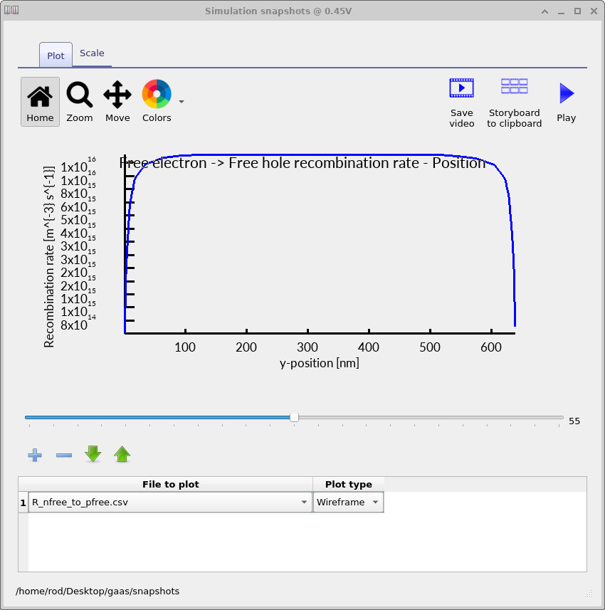
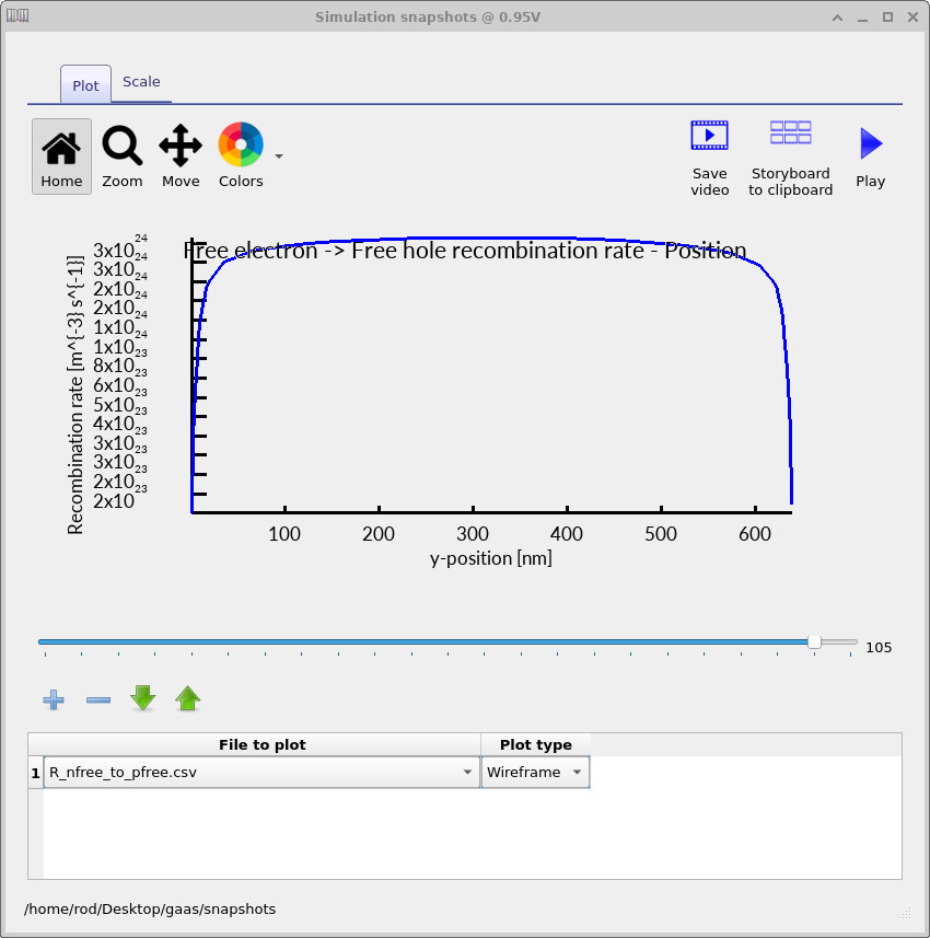
6.4 Free-to-free (radiative) recombination in the active region
Free-to-free recombination can be examined by plotting R_nfree_to_pfree.csv,
which reports the local radiative recombination rate as a function of position.
In GaAs, this channel is typically the dominant recombination mechanism in the active junction under forward bias,
because GaAs is a direct-bandgap semiconductor and radiative transitions are efficient.
When interpreting these plots, the most important feature is not fine spatial structure,
but the global shape of the recombination profile and how its magnitude evolves with bias.
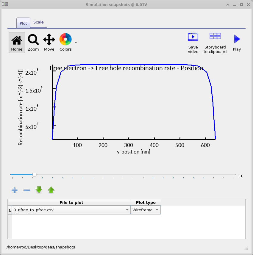
At very low bias (Figure ??), free-to-free recombination is weak because the device is close to equilibrium and the carrier product \(np\) remains close to \(n_i^2\). Although GaAs supports efficient radiative transitions, the carrier densities required to drive a large radiative rate are not yet present.
As the diode is driven into forward bias (Figure ??), injected electrons and holes coexist across most of the structure. The resulting free-to-free recombination profile takes on a broad, gently curved “cap” shape that spans nearly the entire device. This shape reflects the fact that radiative recombination depends primarily on the local carrier product \(np\), which is relatively uniform throughout the quasi-neutral regions once injection is established. Unlike SRH recombination, there is no strong localisation to the depletion region.
At high forward bias (Figure ??), the shape of the free-to-free recombination profile remains broadly similar, while its magnitude increases by many orders of magnitude. This is a key diagnostic feature of radiative-dominated recombination in GaAs: increasing bias primarily raises the carrier densities everywhere, rather than changing where recombination occurs. The smooth, device-spanning profile indicates that radiative recombination is acting as a volume process throughout the injected regions.
This behaviour contrasts strongly with defect-mediated recombination. SRH recombination typically produces narrow, junction-centred peaks that broaden only at high injection, whereas free-to-free recombination in GaAs produces a single, extended recombination “dome” whose height — not its spatial extent — encodes the injection level. In direct-bandgap devices, this broad radiative profile is therefore a signature of high material quality and efficient carrier injection, and it often provides the dominant contribution to the recombination balance that shapes the I–V characteristic.
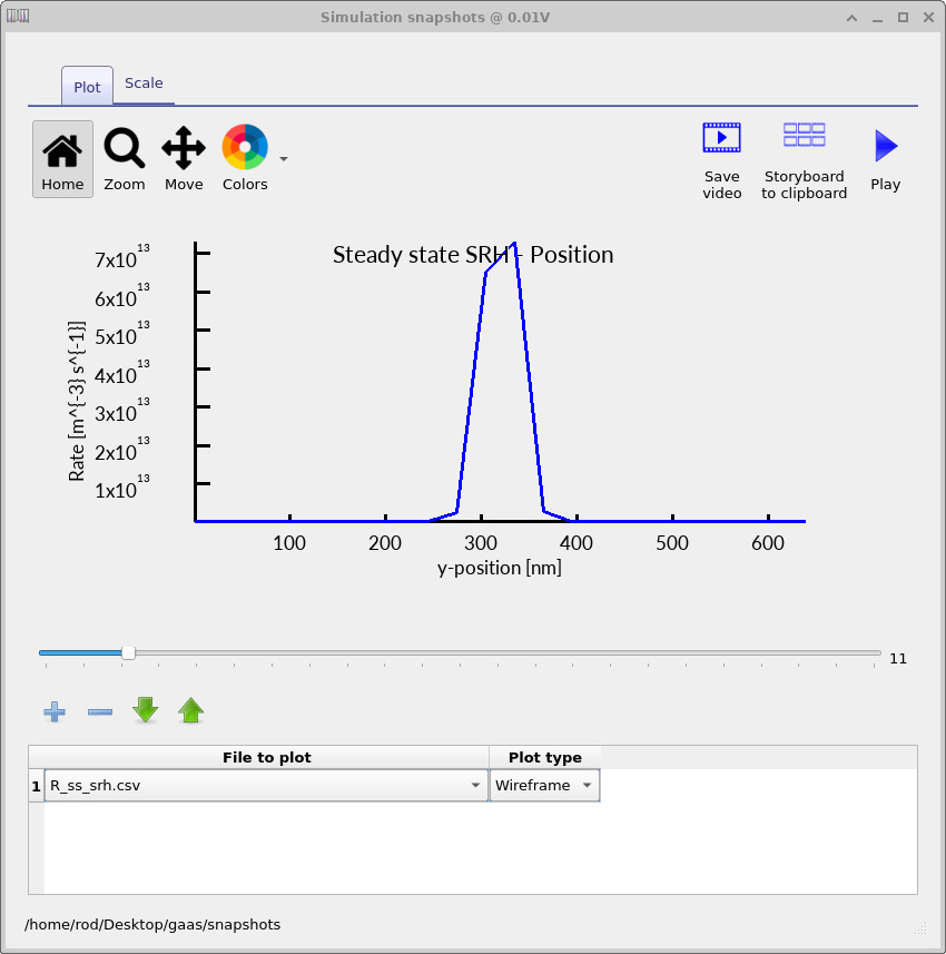
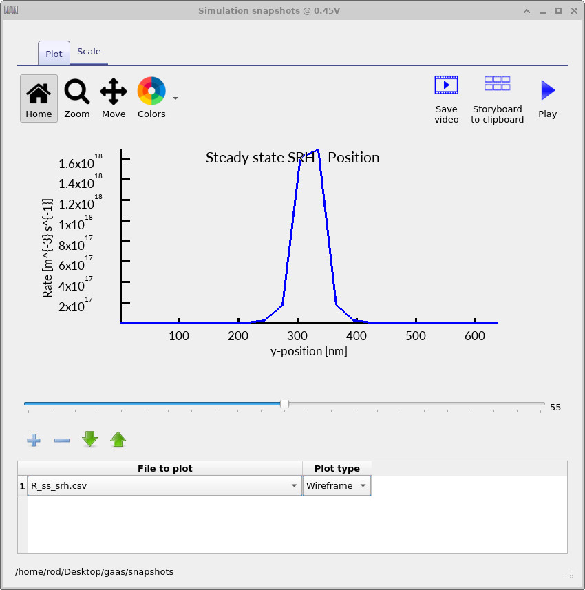
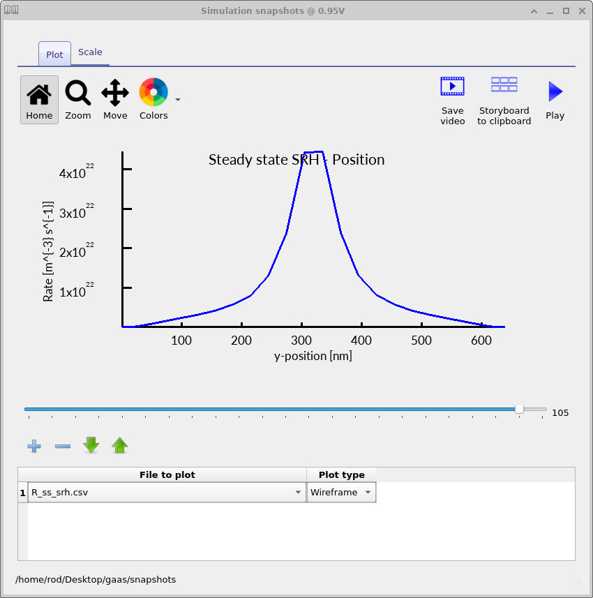
6.2 Shockley–Read–Hall recombination
To examine defect-mediated recombination, plot R_ss_srh.csv, which shows the spatially resolved
Shockley–Read–Hall recombination rate inside the diode.
The three plots below correspond to the same bias points used in the band-diagram analysis:
−0.1 V, ≈0.45 V, and 0.8 V.
For GaAs, these plots are best interpreted as a diagnostic of trap-assisted loss rather than the dominant recombination channel in a high-quality junction.
The key point to focus on is how the spatial localisation of SRH recombination compares with the broader free-to-free profile above.
At −0.1 V (Figure ??), the diode is close to equilibrium. Electrons dominate the n-type side and holes dominate the p-type side, so significant SRH recombination can only occur in the narrow region around the junction where both carrier types are present simultaneously. As a result, the SRH recombination rate is strongly localised at the centre of the device, coinciding with the depletion region. At ≈0.45 V (Figure ??), forward bias injects carriers across the junction and increases the local product of electron and hole densities. The SRH peak grows substantially in magnitude, but it remains spatially confined to the central region of the device. This indicates that SRH remains a junction-centred loss channel, controlled by carrier overlap and trap activity in and near the depletion region. At 0.8 V (Figure ??), the behaviour broadens as carrier injection increases throughout the structure. However, even when SRH spreads, it typically remains more strongly weighted toward the junction region than free-to-free recombination, which tends to be distributed across the injected quasi-neutral regions in GaAs.
Comparing the two recombination channels gives a useful internal picture of GaAs diode operation. Free-to-free recombination provides a volumetric sink once injection is established, and it commonly dominates the overall recombination balance in the active device volume. SRH recombination, by contrast, highlights where trap-assisted loss is concentrated—often in and near the depletion region—making it a sensitive indicator of material quality and interface damage. This distinction helps explain why GaAs diodes can show strong injection and large currents while still being highly sensitive to defects at the junction.
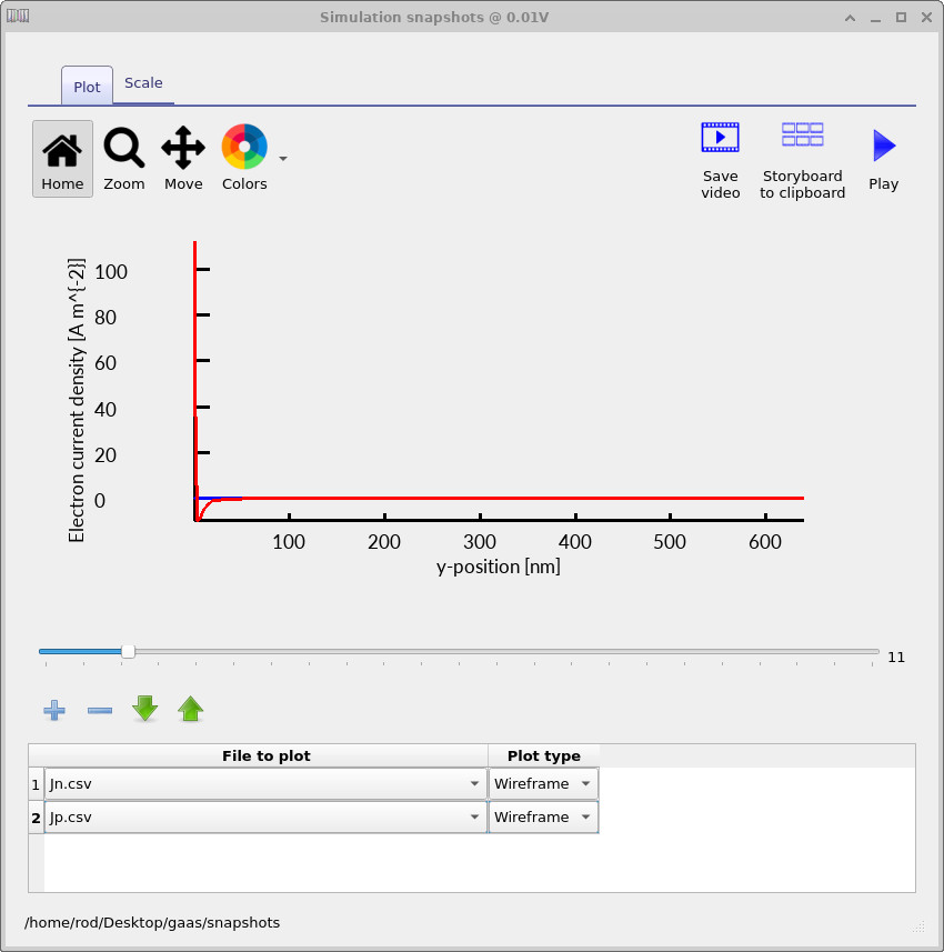
6.3 Electron and hole current densities
Finally, inspect the carrier currents by plotting Jn.csv and Jp.csv,
which show the spatially resolved electron and hole current densities respectively.
These plots provide a direct view of how charge is transported through the diode
under different bias conditions and how the device transitions from equilibrium
to steady-state forward conduction.
At −0.1 V (Figure
??),
the diode is close to equilibrium and the true physical current is extremely small.
Electron and hole fluxes are nearly balanced everywhere in the device,
so the net current arises from the difference of two almost equal quantities.
In this regime the numerical problem is intrinsically ill-conditioned,
and small oscillations or apparent noise in the current profiles are expected.
In this GaAs demo the effect can look more pronounced: the combination of very fast carrier transport
(especially for electrons) and extremely small net current makes the cancellation problem sharper,
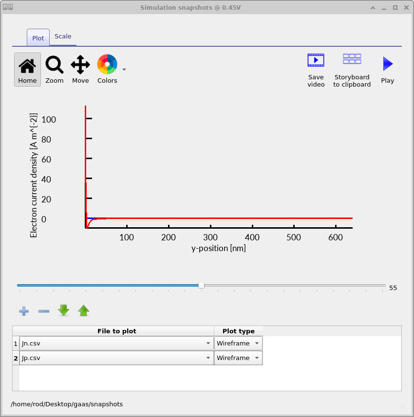
so the raw Jn/Jp traces can appear visibly noisy even though the underlying physics is simply “almost zero current”. At ≈0.45 V (Figure
??),
forward bias drives carrier injection across the junction.
Electron current dominates on the n-side and hole current dominates on the p-side,
but both currents are continuous through the device,
reflecting steady-state charge conservation.
The current density increases rapidly compared to the near-equilibrium case,
yet the profiles can still show small numerical structure near the junction where gradients are steep.
In GaAs, where injection can establish quickly once the barrier is reduced, it is common to see the currents “settle”
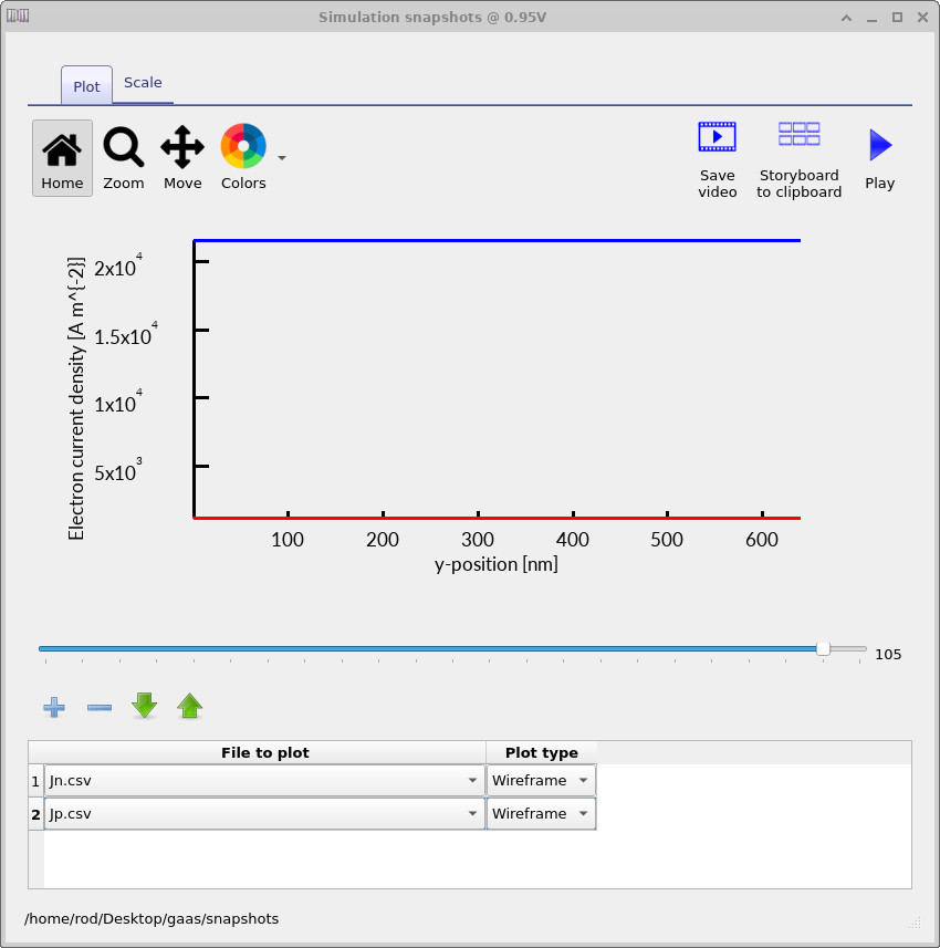
only after the device has moved clearly out of the cancellation-dominated low-current regime. At 0.8 V (Figure
??),
the diode operates deep in forward bias.
Carrier densities are high throughout the structure,
and both electron and hole currents become large, smoother, and more nearly uniform
across the quasi-neutral regions.
Even here, GaAs simulations can retain some residual ripple in the raw current profiles,
particularly if the solver is reporting unfiltered pointwise currents; the key diagnostic is that the large-scale trend is physically consistent,
with continuous current flow and no spurious sign flips through the active device.
Taken together, these current-density plots provide a consistent internal picture of the diode’s operation: from near-perfect cancellation of electron and hole fluxes at equilibrium, through injection-limited forward conduction, to high-current steady-state transport at large forward bias.