PN Junction Diode Simulation (1D): Silicon I–V Curve, Drift–Diffusion & SRH Recombination
1. Introduction
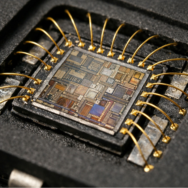
The silicon PN junction diode is the canonical semiconductor device. It appears explicitly as a discrete component and implicitly throughout almost every integrated electronic system, from power rectifiers to logic and analogue circuits. A representative application context is shown in ??, where PN junctions are embedded within an integrated circuit rather than used as standalone devices.
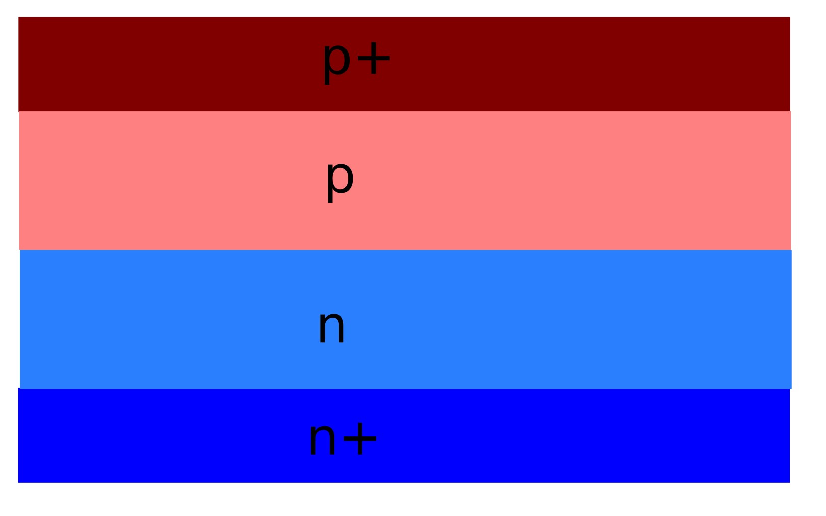
Although the device simulated in this tutorial is simple, it should be understood as a primitive building block. The same junction physics governs diode-connected devices, transistor junctions, and isolation structures inside integrated silicon technologies. The layered doping structure used here is illustrated schematically in ??.
In this tutorial you will simulate a silicon PN junction diode in one dimension using OghmaNano’s coupled drift–diffusion + Poisson solver. Rather than relying solely on the ideal Shockley equation, this approach resolves the built-in electric field, the depletion region, and the spatial distributions of carrier densities and currents.
The explicit treatment of recombination physics—in particular Shockley–Read–Hall (SRH) recombination—makes it possible to connect changes in doping and lifetime directly to changes in turn-on behaviour and ideality. You will generate a dark I–V curve, inspect band edges and quasi-Fermi levels under bias, and then perform a lifetime sweep to identify recombination-limited regimes in the diode response.
2. Making a New Simulation
To begin, create a new simulation from the main OghmaNano window. Click on the New simulation button in the toolbar. This opens the simulation-type selection dialog (see ??).

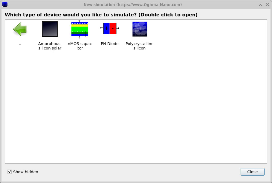
In the simulation-type dialog, double-click on Si demos, then select the silicon junction/diode example (see ??). OghmaNano will load a predefined silicon junction structure which we will treat as a PN diode.
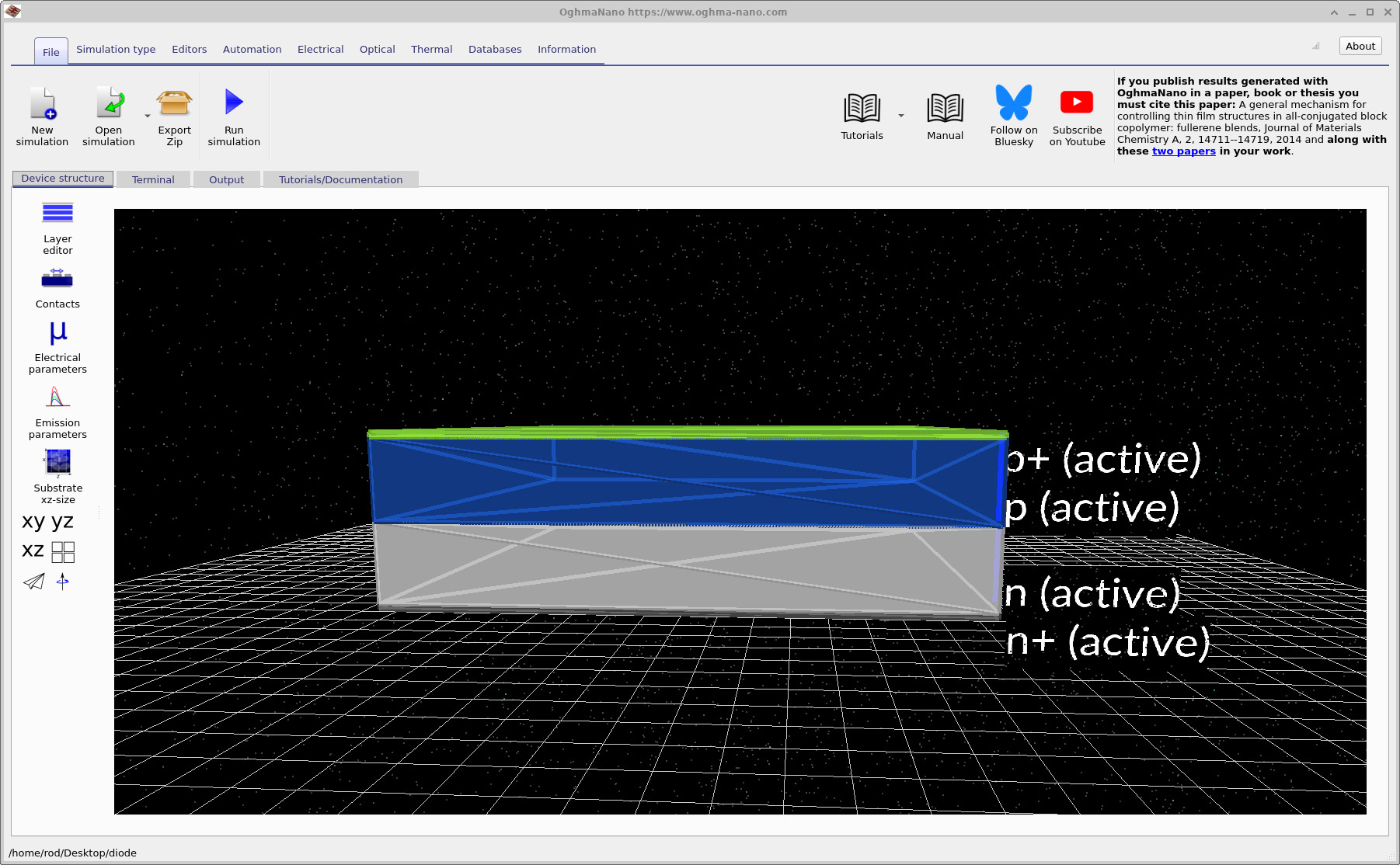
The loaded device structure is shown in the main simulation window (see ??). Although the electrical problem solved in this tutorial is one-dimensional, the 3D view provides a clear visualisation of the vertical layer stack and the regions that participate in carrier transport and recombination.
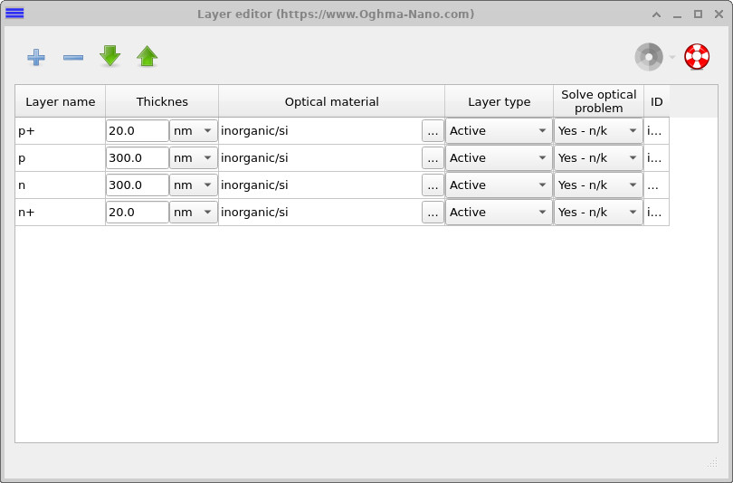
The diode is implemented as a sequence of vertically stacked silicon layers, consisting of a heavily doped p+ region, a more lightly doped p region, a lightly doped n region, and a heavily doped n+ region. This structure is listed explicitly in the Layer editor (see ??), where each layer is assigned a thickness, material, and electrical role.
The central p and n layers form the active PN junction. At equilibrium, a depletion region develops across this interface, giving rise to the built-in electric field that controls carrier separation and transport. The thin, heavily doped p+ and n+ layers act as low-resistance contact regions, ensuring that the applied bias primarily drops across the junction rather than at the contacts.
In the sections that follow, this structure will be treated as a one-dimensional device: all variations are resolved along the growth direction, while lateral variations are neglected. Despite this simplification, the model captures the essential electrostatics, carrier transport, and recombination physics that govern the dark I–V behaviour of silicon PN junction diodes embedded in practical electronic devices.
3. Examining the doping profile
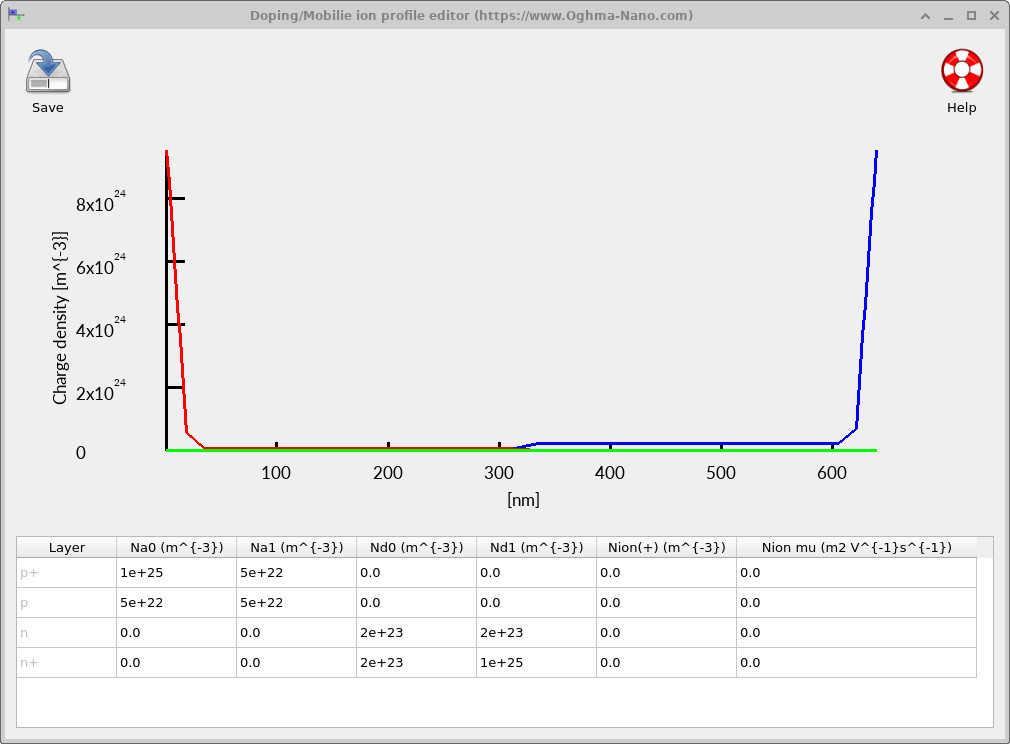
The doping profile defines the silicon PN junction and therefore sets the fundamental electrostatics of the diode. It determines the junction position, the built-in potential, the depletion width, and the internal electric field that develops in equilibrium and under bias.
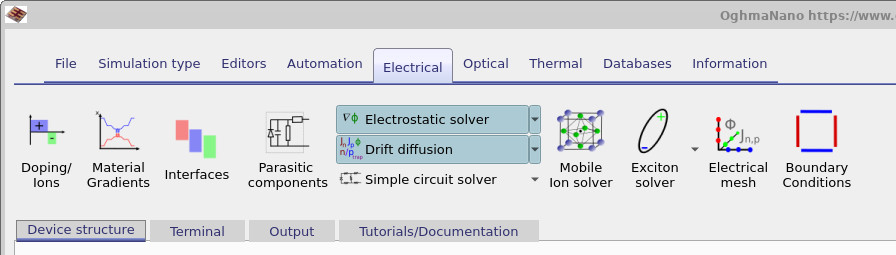
To view the doping configuration, open the Doping / Ions editor from the Electrical ribbon (see ??). The editor displays the spatial distribution of ionised donors and acceptors as a function of depth (see ??).
In this tutorial, the diode is constructed using a conventional p+/p/n/n+ silicon doping profile. The central p and n regions are moderately doped and form the active PN junction, where the depletion region and built-in electric field develop.
The thin, heavily doped p+ and n+ layers act as low-resistance contact regions. Their role is to provide good electrical injection and extraction of carriers, while ensuring that most of the applied voltage drops across the junction itself rather than at the contacts.
For the purposes of this tutorial, the key check is simply that the device contains one predominantly acceptor-doped region and one predominantly donor-doped region, with a clear transition between them. The exact numerical values of the doping densities primarily affect the depletion width and built-in field strength, which will be explored indirectly through the diode’s dark I–V characteristics in later sections.
4. Examining electrical parameters and recombination mechanisms
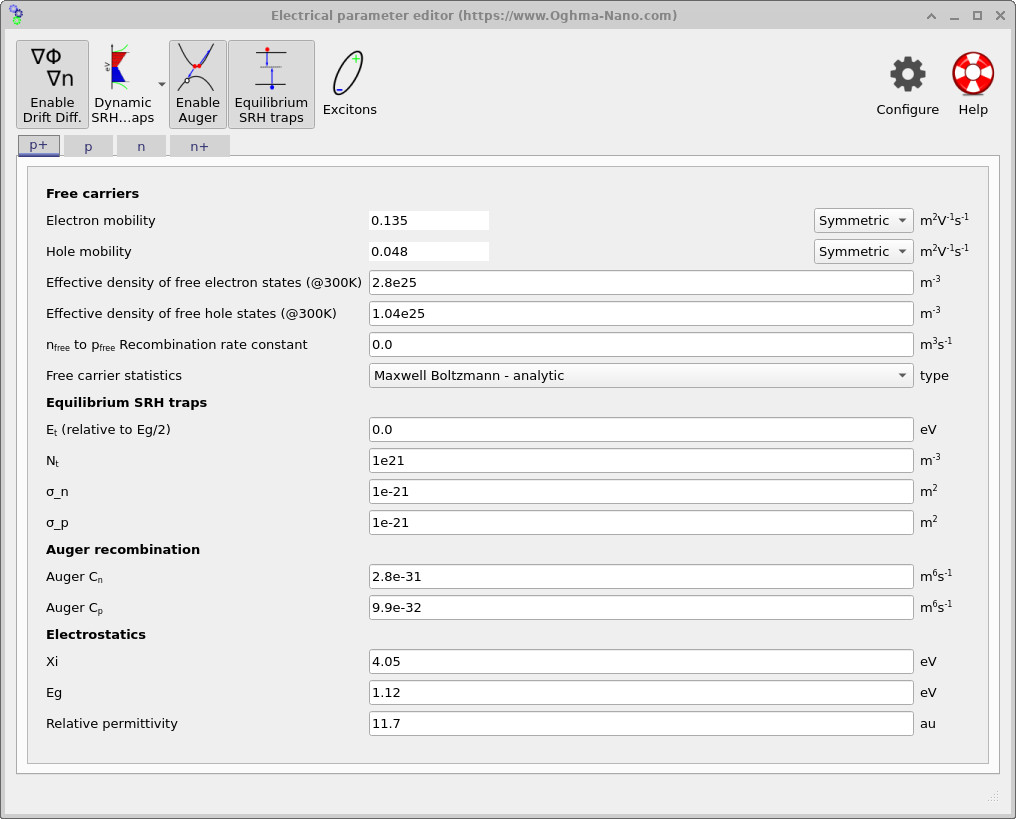
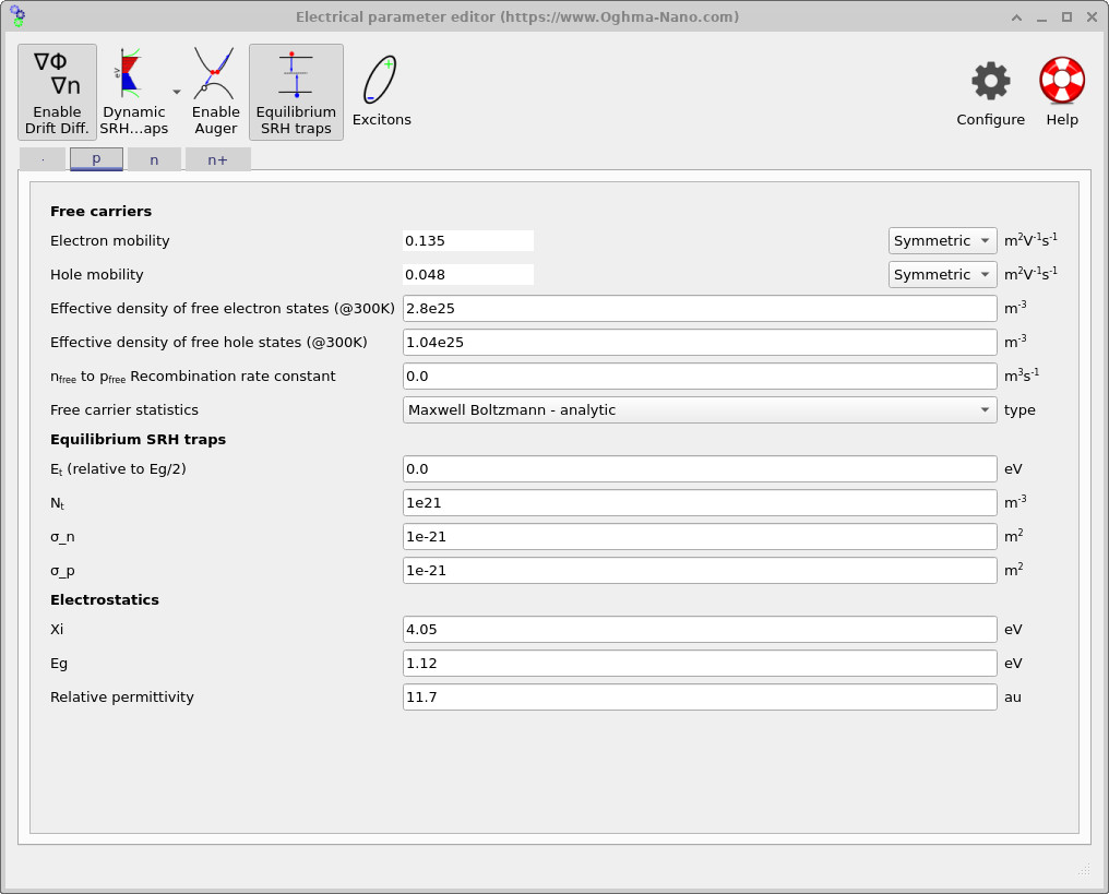
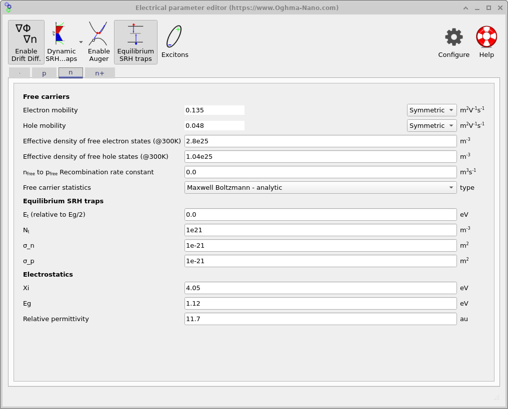
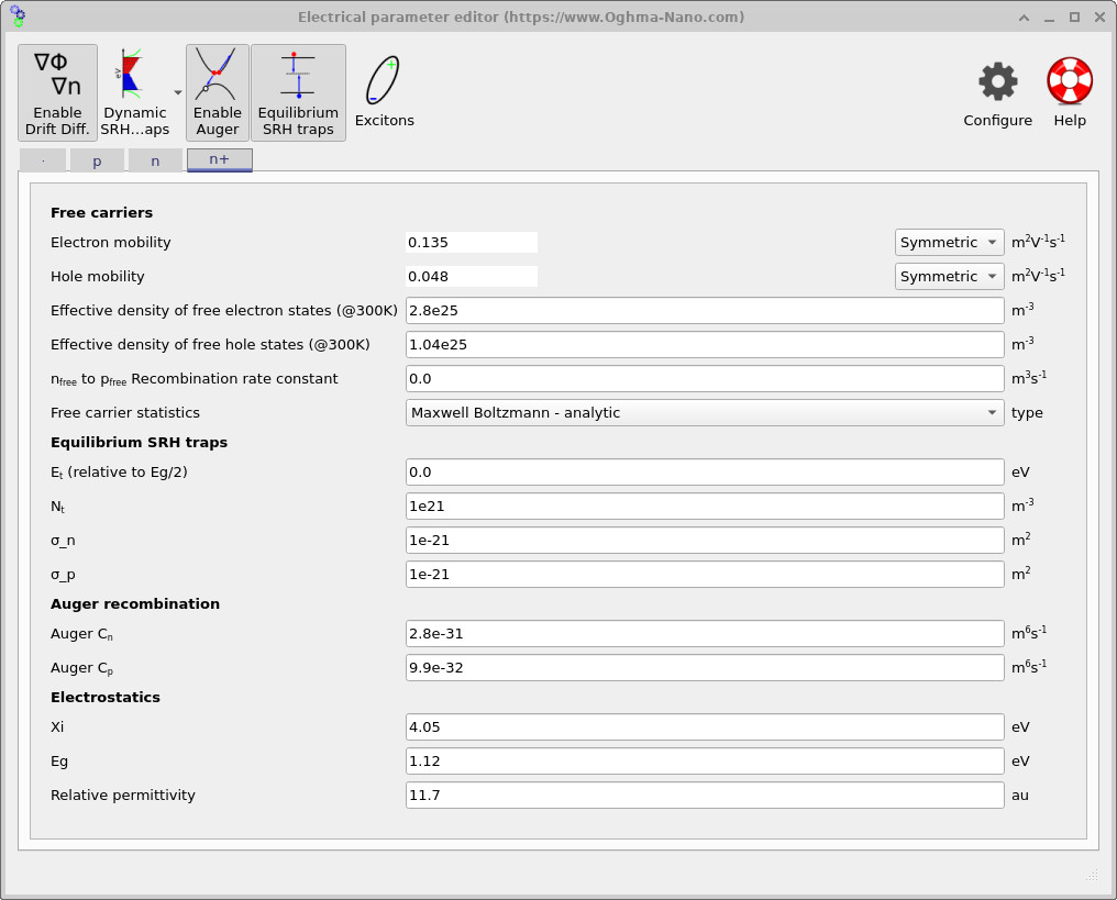
Electrical material parameters are defined on a per-region basis and control carrier transport, recombination, and electrostatics throughout the diode. Open the electrical parameter editor from the main window via Device structure → Electrical parameters. Each layer in the device stack has its own parameter tab. In this tutorial we use the same silicon material model in all four regions, but we interpret them differently: p+ and n+ act as low-resistance contact regions, while p and n form the active junction.
Figures ??– ?? show the electrical parameter editor for each region (p+, p, n, n+). In this demo the electron and hole mobilities are set to approximately 0.135 and 0.048 m2V−1s−1, respectively (see, for example, ??). These values are typical of crystalline silicon: they are much higher than those found in disordered or defect-limited materials such as amorphous silicon or many solution-processed semiconductors, but lower than in high-mobility III–V materials like GaAs. As a result, the diode behaviour in this tutorial is primarily controlled by junction electrostatics and recombination, rather than by bulk transport limitations.
The effective densities of states used here are also visible in the editor (e.g. ??): the effective free-electron density of states is set to approximately 2.8×1025 m−3 and the effective free-hole density of states to 1.04×1025 m−3. These parameters set the carrier statistics and equilibrium carrier concentrations for a given band structure, and they enter implicitly into recombination and injection behaviour through \(n\) and \(p\).
Shockley–Read–Hall (SRH) recombination
Shockley–Read–Hall (SRH)recombination captures defect-mediated recombination through electronic states in the bandgap. In OghmaNano this is controlled using the equilibrium SRH trap parameters shown in the editor (see ??): a trap energy \(E_t\) (relative to midgap), a trap density \(N_t\), and electron and hole capture cross-sections \(\sigma_n\) and \(\sigma_p\). For the settings shown here, the trap energy lies close to midgap (\(E_t \approx 0\)), the trap density is \(N_t \approx 10^{21}\,\mathrm{m^{-3}}\), and the capture cross-sections are \(\sigma_n \approx \sigma_p \approx 10^{-21}\,\mathrm{m^2}\).
These microscopic parameters define the SRH lifetimes via
\[ \tau_n = \frac{1}{\sigma_n v_{\mathrm{th}} N_t}, \qquad \tau_p = \frac{1}{\sigma_p v_{\mathrm{th}} N_t}, \]where \(v_{\mathrm{th}}\) is the thermal carrier velocity. Increasing the trap density or capture cross-sections therefore reduces the carrier lifetime and enhances recombination.
In drift–diffusion form, the resulting SRH recombination rate is
\[ R_{\mathrm{SRH}} = \frac{np - n_i^2} {\tau_p (n + n_1) + \tau_n (p + p_1)} . \]In later sections, when you “sweep the lifetime”, you are effectively modifying the trap-assisted recombination strength encoded by \(N_t\), \(\sigma_n\), and \(\sigma_p\). The strongest impact is observed when recombination in and near the depletion region controls the injected carrier population, leading to recombination-limited forward-bias behaviour.
Auger recombination
Auger recombination is a high-carrier-density loss mechanism and is therefore most relevant in the heavily doped p+ and n+ contact regions. In the parameter editor, the Auger coefficients \(C_n\) and \(C_p\) are specified (see ?? and ??). For this silicon demo, the coefficients are on the order of \(C_n \approx 2.8\times10^{-31}\,\mathrm{m^6\,s^{-1}}\) and \(C_p \approx 9.9\times10^{-32}\,\mathrm{m^6\,s^{-1}}\), which are typical values for crystalline silicon.
The Auger recombination rate is given by
\[ R_{\mathrm{Auger}} = C_n n^2 p + C_p p^2 n . \]In practice, Auger recombination limits carrier accumulation at high injection and ensures that the contact regions behave as efficient sinks for carriers, without dominating the recombination physics in the moderately doped junction itself.
Electrostatics and band parameters
Finally, the band-structure and electrostatic parameters used to define silicon are visible in each region tab (e.g. ??): the electron affinity is set to approximately \(\chi \approx 4.05\,\mathrm{eV}\), the bandgap to \(E_g \approx 1.12\,\mathrm{eV}\), and the relative permittivity to \(\varepsilon_r \approx 11.7\).
5. Running the simulation, dark I–V curves, and extracting parameters
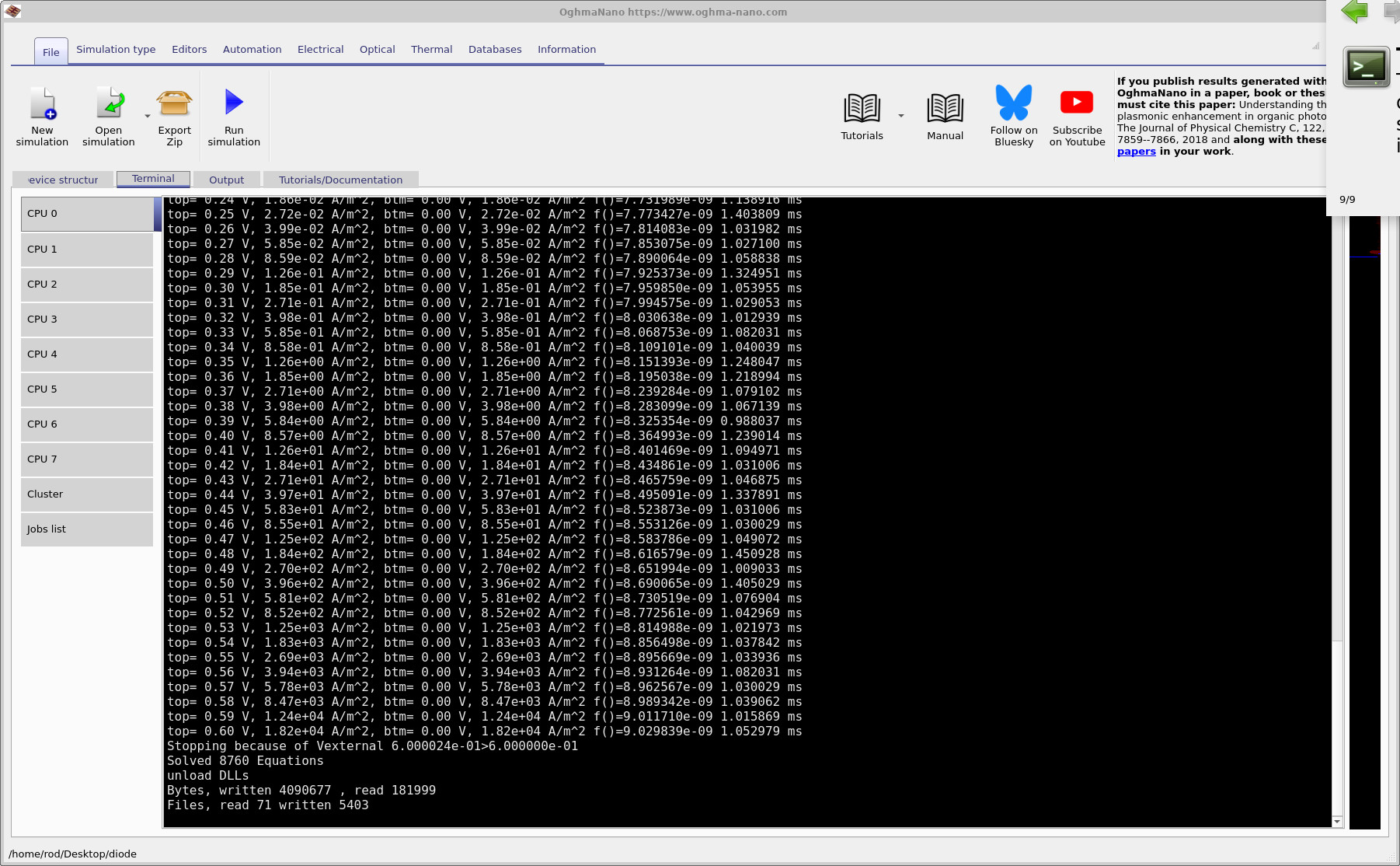
Once the device structure, doping profile, and electrical parameters are defined, the diode simulation can be run directly from the main window. Click Run simulation to start the solver. During execution, convergence information for each bias point is written to the terminal, allowing you to monitor solver stability and progress (see ??).
jv.csv is the primary result of interest.
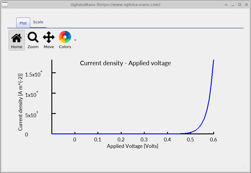
To inspect the diode characteristic, open the Output tab and double-click
jv.csv
(see ??).
For a correctly configured silicon diode, the I–V curve should be smooth and monotonic.
In reverse bias, the current remains small and weakly voltage-dependent,
reflecting recombination-limited saturation.
In forward bias, the current increases rapidly with applied voltage,
corresponding to carrier injection across the PN junction.
The shape of the forward-bias region contains useful physical information. On a semi-logarithmic plot, the slope of the exponential region can be used to extract an ideality factor, indicating whether the current is dominated by diffusion-limited transport (\(n \approx 1\)) or recombination-limited processes (\(n \approx 2\)). The extrapolated intercept of this region provides an estimate of the reverse saturation current, which is directly linked to the SRH and Auger recombination parameters discussed in Section 4.
As a practical rule, always inspect the I–V curve before interpreting any derived quantities. Discontinuities, unexpected sign conventions, or non-physical jumps in current usually indicate issues with boundary conditions, bias stepping, recombination settings, or solver convergence. For a simple silicon PN diode such as this, the dark I–V curve should be physically intuitive and easy to interpret.
6. Examining simulation snapshots: bands, recombination, and current flow
During an I–V sweep, OghmaNano stores the internal solution of the drift–diffusion equations at each bias point in the snapshots directory. These files expose what the solver is predicting inside the diode: band bending, quasi-Fermi level splitting, recombination activity, and current transport. Examining these quantities is essential for understanding why a particular I–V characteristic emerges.
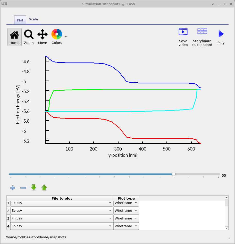
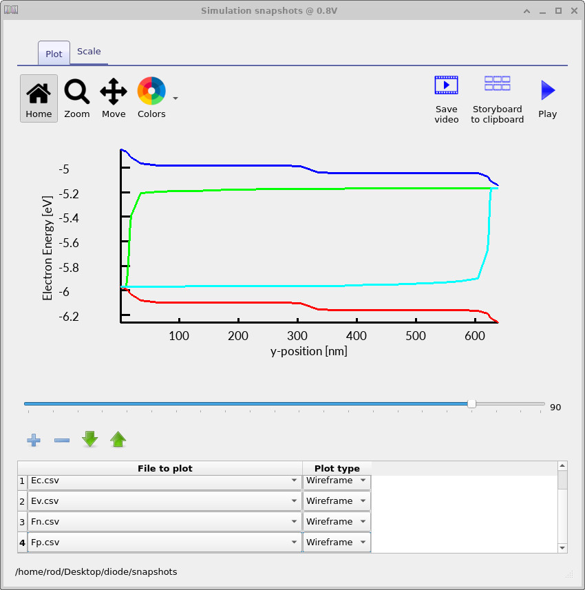
In this section we inspect three representative bias points: a near-equilibrium reverse bias (−0.1 V), a moderate forward bias near turn-on (≈0.45 V), and a high forward bias (0.8 V). Together, these snapshots illustrate the transition from equilibrium, through injection-limited transport, to high-injection operation.
6.1 Band edges and quasi-Fermi levels
To reproduce the band diagrams, open the snapshot viewer and add the files
Ec.csv, Ev.csv, Fn.csv, and Fp.csv.
These correspond to the conduction band edge, valence band edge,
electron quasi-Fermi level, and hole quasi-Fermi level respectively.
At −0.1 V (Figure ??), the diode is close to equilibrium. The band bending reflects the built-in potential imposed by the doping profile, and the quasi-Fermi levels are nearly flat and coincident, indicating negligible net current flow. The depletion region is clearly visible as the region of strong band curvature at the junction. At ≈0.45 V (Figure ??), forward bias reduces the junction barrier. The electron and hole quasi-Fermi levels split across the depletion region, which is the internal signature of carrier injection. This quasi-Fermi level separation is directly responsible for the exponential rise in current observed in the I–V curve. At 0.8 V (Figure ??), the junction is deep into forward bias. The barrier is strongly suppressed, the quasi-Fermi levels are widely separated, and the device operates in a high-injection regime where carrier densities are large throughout much of the structure.

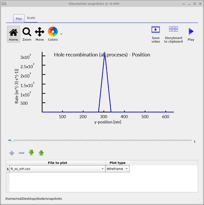
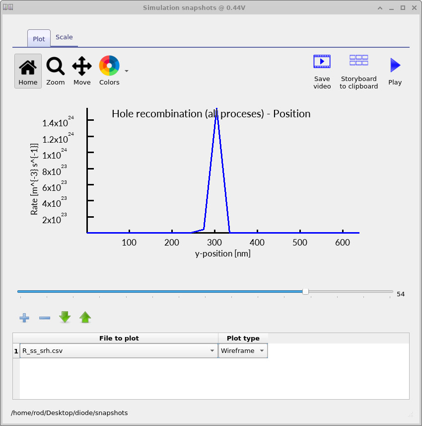
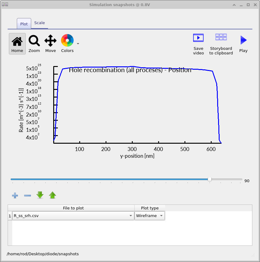
6.2 Shockley–Read–Hall recombination
To examine recombination, plot R_ss_srh.csv, which shows the spatially resolved
Shockley–Read–Hall recombination rate inside the diode.
The three plots below correspond to the same bias points used in the band-diagram analysis:
−0.1 V, ≈0.45 V, and 0.8 V.
The key point to focus on is not the absolute magnitude of the recombination rate,
but how its spatial localisation changes with applied bias.
At −0.1 V (Figure ??), the diode is close to equilibrium. Electrons dominate the n-type side and holes dominate the p-type side, so significant recombination can only occur in the narrow region around the junction where both carrier types are present simultaneously. As a result, the SRH recombination rate is strongly localised at the centre of the device, coinciding with the depletion region. At ≈0.45 V (Figure ??), forward bias injects carriers across the junction and increases the local product of electron and hole densities. The recombination peak grows substantially in magnitude, but it remains spatially confined to the central region of the device. This indicates that, in this bias range, SRH recombination is still primarily a junction-centred process, controlled by carrier overlap in and near the depletion region. At 0.8 V (Figure ??), the behaviour changes qualitatively. Carrier injection is sufficiently strong that both electrons and holes are present in high concentrations throughout much of the diode. The SRH recombination rate is no longer confined to the junction, but spreads across a large fraction of the device. This spatial broadening signals the onset of high-injection conditions, where recombination is no longer limited to a narrow central region.
The progression from a sharply localised recombination peak to a spatially extended recombination profile provides a clear internal picture of how the diode transitions from equilibrium, through junction-limited operation, to a regime where recombination occurs throughout the structure. This evolution mirrors the changes seen in the band diagrams and underpins the change in slope of the forward I–V characteristic.
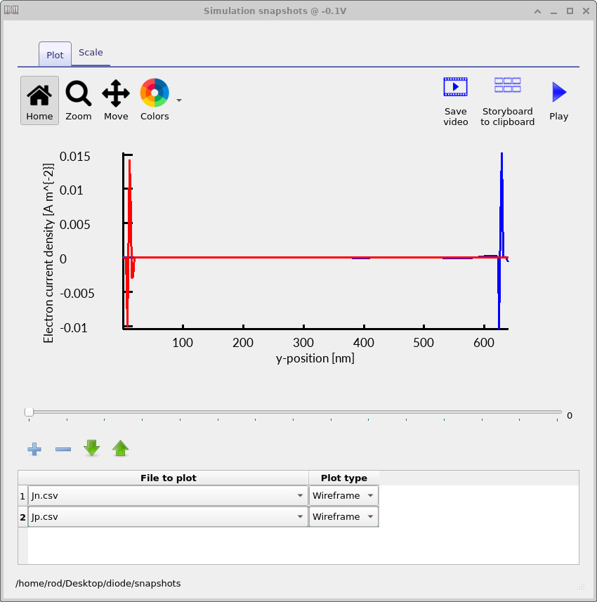
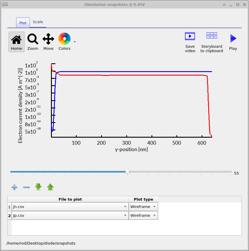
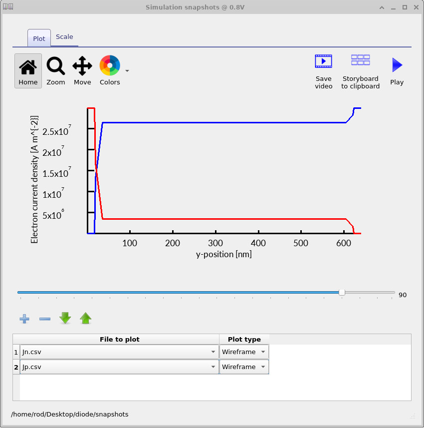
6.3 Electron and hole current densities
Finally, inspect the carrier currents by plotting Jn.csv and Jp.csv,
which show the spatially resolved electron and hole current densities respectively.
These plots provide a direct view of how charge is transported through the diode
under different bias conditions and how the device transitions from equilibrium
to steady-state forward conduction.
At −0.1 V (Figure ??), the diode is close to equilibrium and the true physical current is extremely small. Electron and hole fluxes are nearly balanced everywhere in the device, so the net current arises from the difference of two almost equal quantities. In this regime the numerical problem is intrinsically ill-conditioned, and small oscillations or apparent noise in the current profiles are expected. These features are numerical in origin and do not correspond to real carrier transport. At ≈0.45 V (Figure ??), forward bias drives carrier injection across the junction. Electron current dominates on the n-side and hole current dominates on the p-side, but both currents are continuous through the device, reflecting steady-state charge conservation. The current density increases rapidly compared to the near-equilibrium case, yet remains spatially structured near the junction, consistent with injection-limited transport controlled by recombination. At 0.8 V (Figure ??), the diode operates deep in forward bias. Carrier densities are high throughout the structure, and both electron and hole currents become large, smooth, and nearly uniform across the quasi-neutral regions. In this regime the device behaves as a strongly conducting element, with current limited primarily by transport and recombination rather than barrier injection.
Taken together, these current-density plots provide a consistent internal picture of the diode’s operation: from near-perfect cancellation of electron and hole fluxes at equilibrium, through injection-limited forward conduction, to high-current steady-state transport at large forward bias.
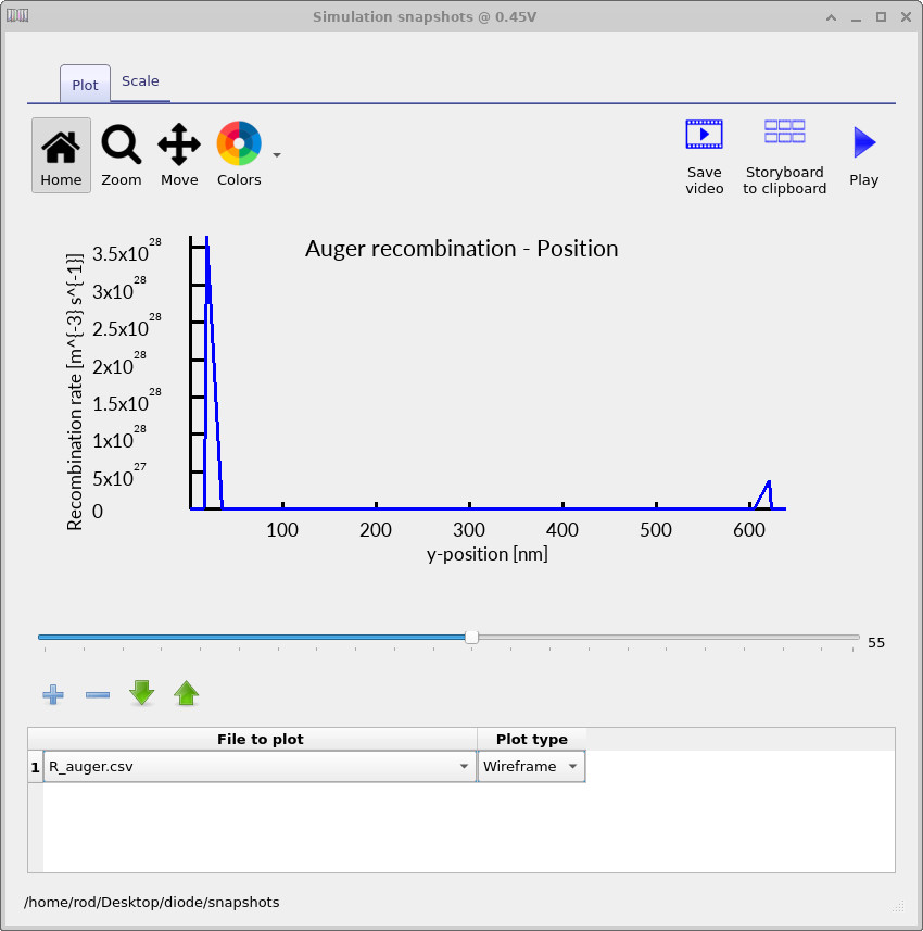
6.4 Auger recombination in heavily doped regions
Auger recombination can be examined by plotting R_auger.csv,
which reports the local Auger recombination rate as a function of position.
Unlike SRH recombination, which is strongest where electrons and holes coexist
at comparable densities, Auger recombination scales strongly with carrier density
and therefore becomes dominant in heavily doped regions.
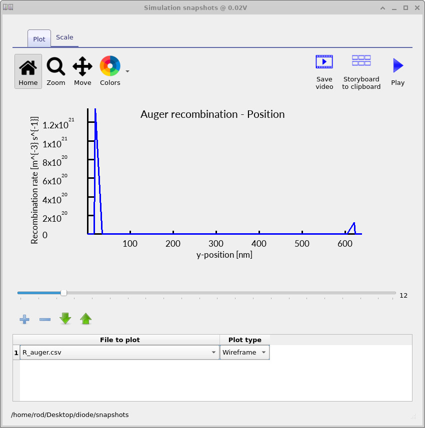

At very low bias (Figure ??), Auger recombination is already visible in the p+ and n+ contact layers. This occurs even near equilibrium because these regions are intentionally heavily doped, resulting in carrier concentrations high enough for three-particle (Auger) processes to dominate locally.
As the diode is driven into forward bias (Figure ??), the Auger recombination rate increases rapidly in magnitude but remains spatially confined to the contact regions. This localisation reflects the strong density dependence of Auger recombination: although carriers are injected across the junction, the highest carrier densities still reside in the degenerate contact layers.
At high forward bias (Figure ??), Auger recombination becomes extremely large in the contacts, dwarfing SRH recombination in magnitude. This behaviour is expected and physically correct. The role of Auger recombination here is not to limit the junction current directly, but to prevent unphysical carrier accumulation in regions where the carrier density would otherwise grow without bound under high injection.
Importantly, although the Auger recombination rate is numerically much larger than the SRH rate, it does not dominate the diode ideality or the turn-on behaviour. Those features are still controlled primarily by recombination in and near the depletion region. Auger recombination instead acts as a high-density stabilisation mechanism in the contact layers, ensuring realistic behaviour at large currents.