Advanced GaAs Device Simulation Software


1. Introduction
OghmaNano provides an advanced GaAs device simulation framework for modelling gallium arsenide structures in 1D, 2D, and 3D using a coupled drift–diffusion + Poisson solver. GaAs is a particularly important semiconductor because of its high electron mobility, direct bandgap, and widespread use in high-speed electronics, lasers, photodiodes, and advanced photovoltaic structures.
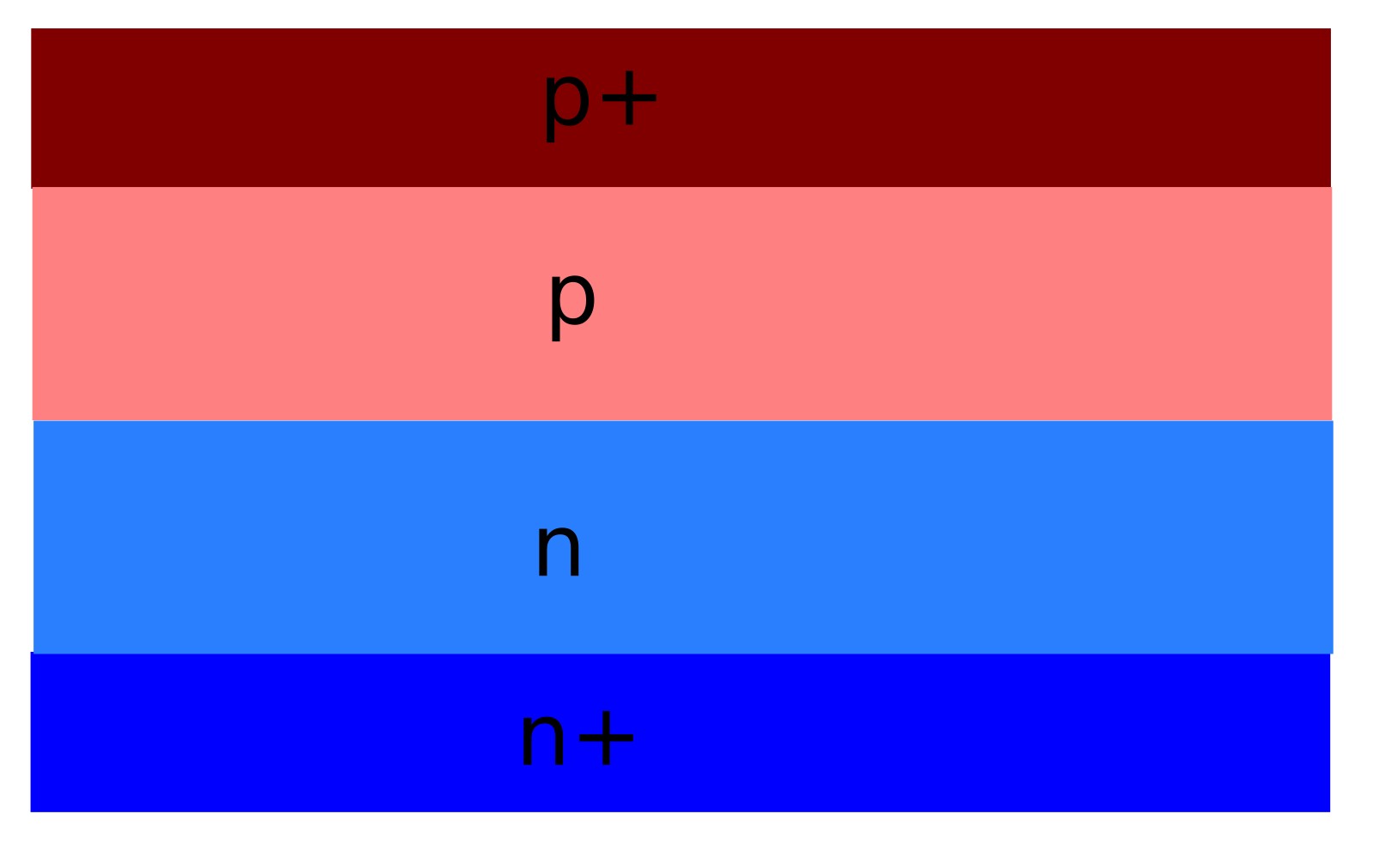
Rather than treating devices as idealised black boxes, OghmaNano resolves the internal state directly: band bending, depletion, quasi-Fermi levels, recombination, defects, carrier flow, and contact effects can all be inspected in space. This makes it possible to understand not just the final I–V curve, but why it takes that shape. A representative GaAs device context is shown in Figure ??, while a typical pn-junction structure is shown in Figure ??.
The same framework can be used for simple 1D pn diodes, 3D defect studies, MOS-capacitor electrostatics, and doped-resistor examples for teaching and research. A standard GaAs junction setup is shown in Figure ??, while a fully 3D defect problem is shown in Figure ??.
✨ What you can do with OghmaNano
- Simulate realistic GaAs pn junctions: study depletion width, built-in potential, dark I–V curves, and recombination-limited behaviour.
- Visualise 3D defects directly: add localised shunts or defect regions and see how they distort current flow and recombination.
- Study ohmic conduction: model doped GaAs resistors with uniform or graded doping and inspect the resulting potential and field distributions.
- Explore gate electrostatics: build MOS-capacitor structures and examine accumulation, depletion, and inversion in space.
- Compare 1D, 2D, and 3D: identify when higher dimensionality adds real physics and when it only adds runtime.
- Inspect internal variables: plot band edges, quasi-Fermi levels, SRH recombination, free-to-free recombination, and current-density components.
- Use GaAs as a teaching platform: demonstrate core semiconductor concepts with structures that are physically clean and visually intuitive.
Try a GaAs example.
👉 Start with the GaAs pn-junction diode tutorial, or jump to the 3D defect tutorial or 3D doped GaAs resistor tutorial.
2. Why GaAs is a useful device-physics platform
GaAs sits in an interesting position for simulation. Its high mobilities make transport fast, while its direct bandgap makes free-to-free recombination particularly relevant in high-quality material. This means GaAs examples often show very clearly how injection, recombination, and electrostatics interact. In a pn diode, for example, reducing the junction barrier leads to strong carrier injection, visible quasi-Fermi level splitting, and rapidly increasing current.
At the same time, GaAs is an excellent platform for showing where simpler models break down. A uniform pn junction can often be understood in 1D, but as soon as a localised defect, finite contact, or lateral inhomogeneity is introduced, the problem becomes genuinely 2D or 3D. That transition is one of the clearest lessons in device simulation, and it can be explored directly in the 3D defect workflow.
3. Core GaAs example workflows
OghmaNano’s GaAs examples are designed to cover three complementary classes of problem.
First, the GaAs pn-junction diode tutorial focuses on the standard 1D problem: doping profiles, depletion, SRH recombination, free-to-free recombination, dark I–V curves, and internal band diagrams. This is the cleanest route into GaAs drift–diffusion modelling and a very good teaching example.
Second, the 3D GaAs defect tutorial introduces a top-to-bottom defect that forces lateral current flow. This is where 3D becomes essential: current crowding, localised recombination, and contact-resolved JV curves appear in ways that cannot be reproduced by a 1D treatment. The follow-up tutorial, Part B, then removes the defect and shows how the same device collapses cleanly back to 3D→2D→1D once the lateral asymmetry disappears.
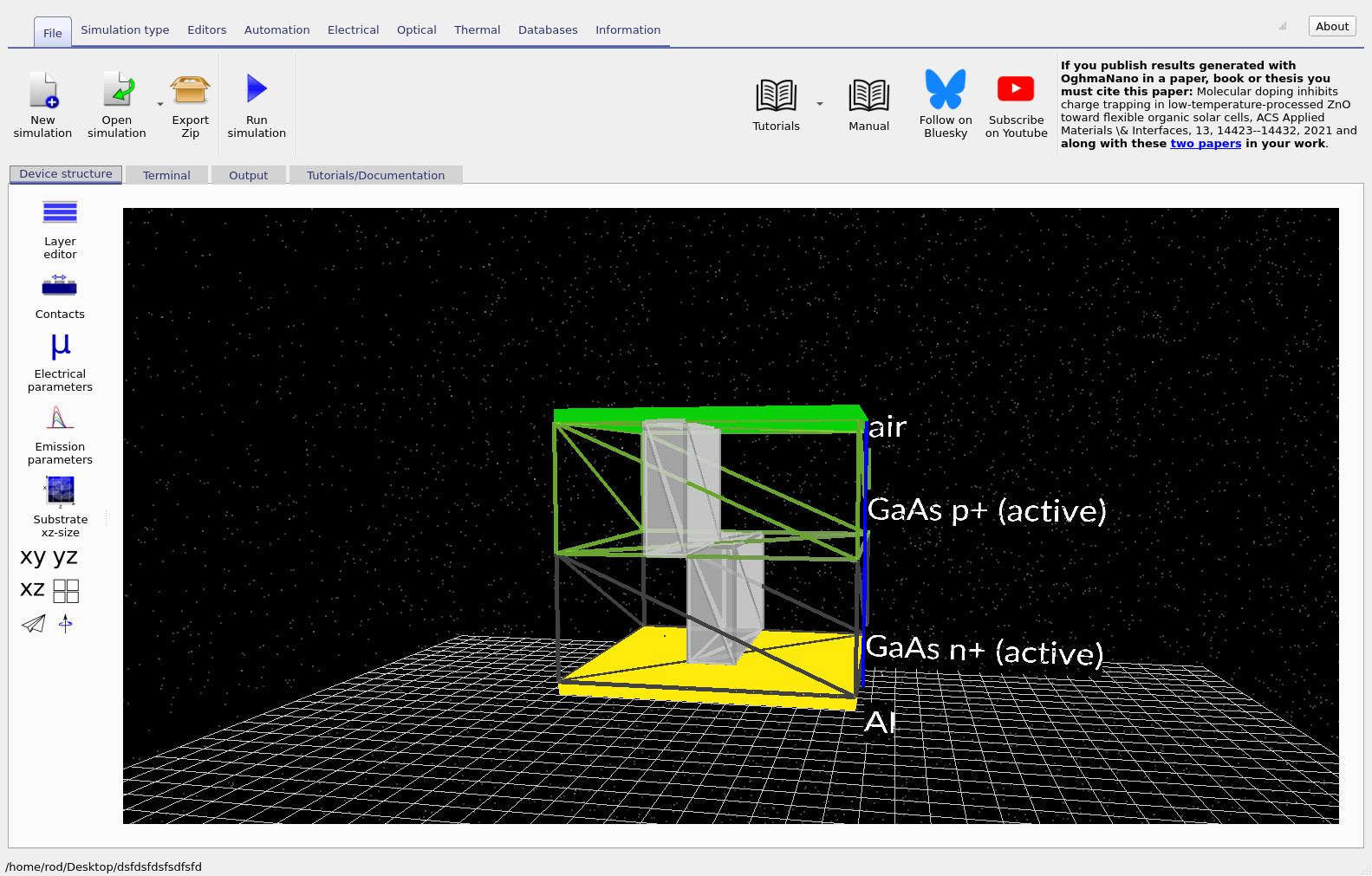
Third, the 3D doped GaAs resistor tutorial provides a simple but very useful example for understanding ohmic conduction, contact geometry, mesh scaling, and current-density visualisation in multidimensional drift–diffusion problems. The corresponding structure is shown in Figure ??.
4. Recombination, defects, and internal visualisation
One of the main advantages of the GaAs examples is that they expose the internal physics clearly. In the pn-junction tutorial, for example, both free-to-free recombination and Shockley–Read–Hall recombination can be plotted as a function of position and bias. This makes it possible to see the difference between broad, injected radiative recombination and more localised defect-mediated loss channels.
Likewise, in 3D examples, the snapshots viewer can be used to inspect current-density components, electrostatic potential, and carrier densities across the full structure. This is particularly valuable for defect problems, where the whole point is that the device is no longer laterally uniform.
For related theory, see: drift–diffusion modelling, Shockley–Read–Hall recombination, free-to-free recombination, and Poisson electrostatics.
5. Teaching, training, and research use
These GaAs demos work well both as research templates and as teaching examples. For teaching, they show how doping, electrostatics, current transport, and dimensionality interact in a semiconductor device. For research, they provide a starting point for modified junctions, local defects, non-uniform doping, contact studies, and more specialised III–V structures.
Because the examples range from clean 1D junctions to genuinely 3D non-uniform devices, they are also useful for teaching an often-missed modelling lesson: use the lowest dimensionality that still contains the physics you need. OghmaNano’s GaAs examples make that lesson unusually explicit.