Large-Area Device Simulation Software
1. Introduction
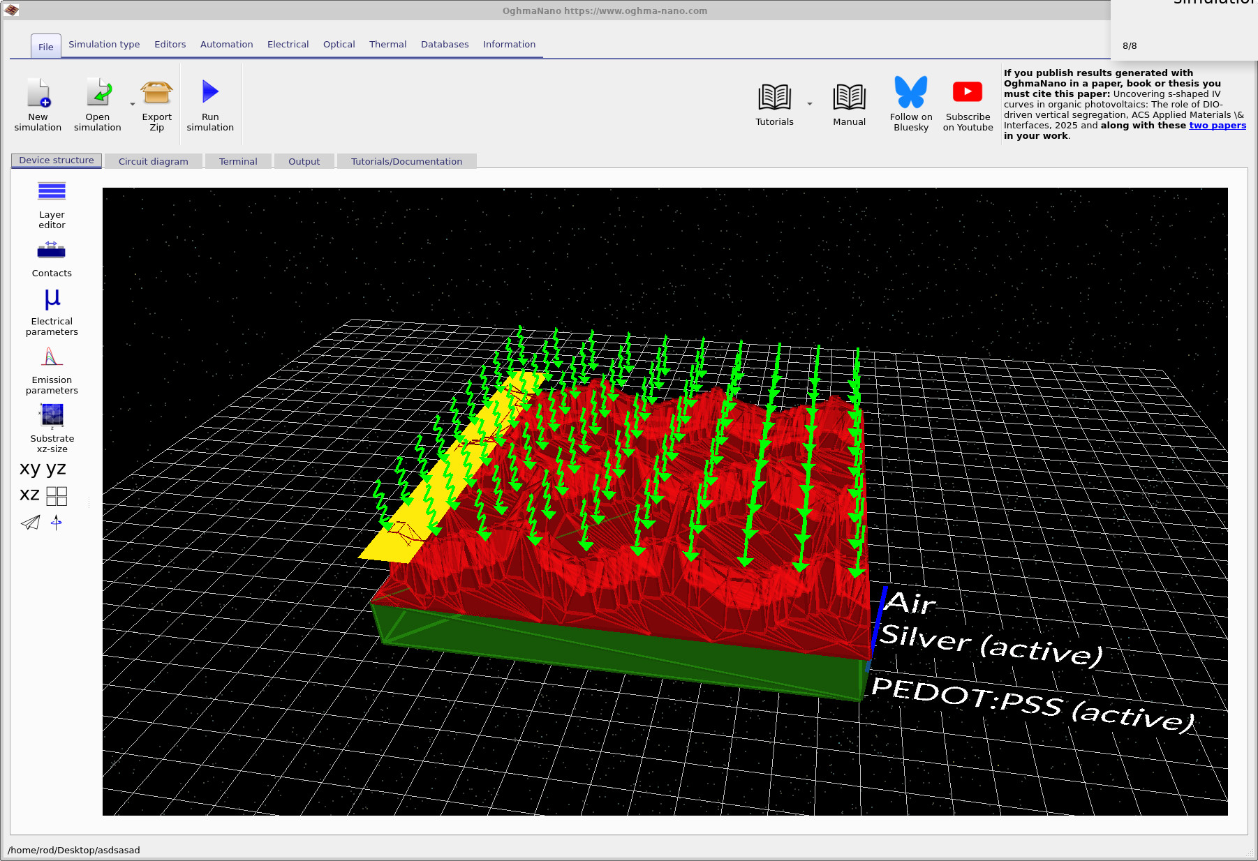
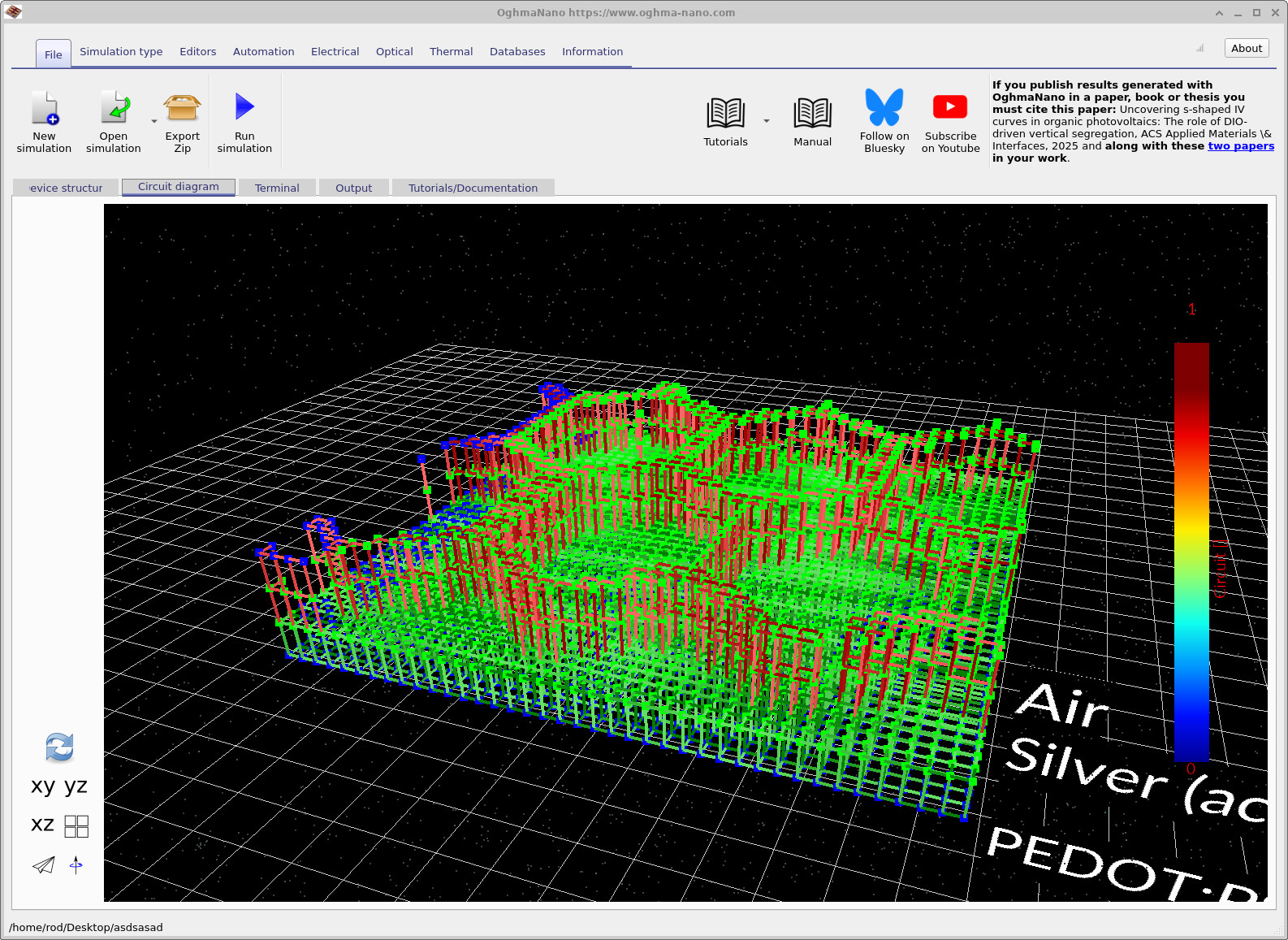
OghmaNano provides a large-area device simulation framework for modelling photovoltaic and optoelectronic structures limited by lateral current flow, contact resistance, and spatial non-uniformity. Instead of solving full 3D drift–diffusion everywhere, it converts the geometry into a spatially resolved resistor–diode network, enabling efficient device- and module-scale simulations. This allows realistic scaling beyond laboratory devices, where losses are dominated by current spreading in transparent conductors, metallic meshes, and contacts rather than vertical transport. OghmaNano solves a geometry-aware 3D circuit built directly from the layout, visualised in Figure ??, with the corresponding circuit representation shown in Figure ??. Arbitrary 3D geometries—such as hexagonal meshes, busbars, and patterned electrodes—can be generated or imported, and analysed for resistance, voltage drop, shading, and current crowding. The same workflow extends from stand-alone contacts to illuminated devices, as demonstrated by the large-area PM6:Y6 example in Figure ??.
A guided introduction is available in Figure ?? and Figure ??. The full workflow begins with Part A: setting up a 3D contact model.
✨ What you can do with OghmaNano
- Build realistic large-area geometries: define metallic meshes, transparent conductors, extraction bars, and custom 3D contact layouts.
- Generate 3D resistor–diode networks automatically: convert the geometry into a circuit model that captures lateral transport and local voltage loss.
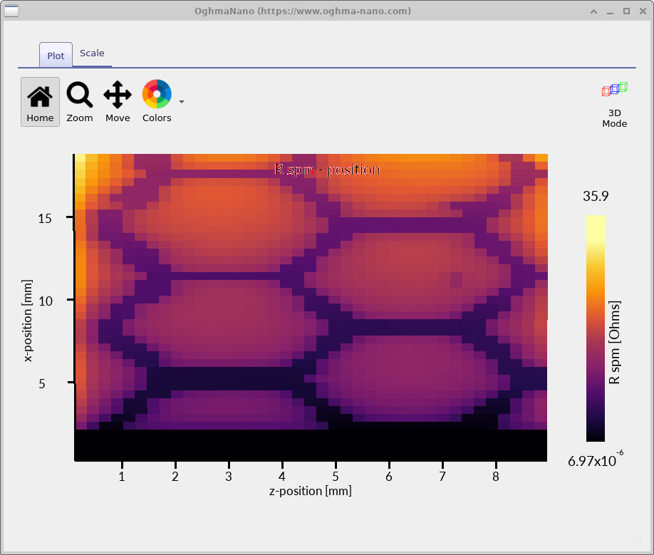
- Map resistance and current spreading: identify which regions of the structure dominate loss, as illustrated by the resistance map in Figure ??.
- Study contact engineering: test how mesh pitch, line width, material resistivity, and extraction geometry affect performance before fabrication.
- Include optical effects and shading: combine the large-area electrical model with optical calculations to study shadowing and non-uniform generation.
- Bridge from contacts to full devices: extend the same workflow from stand-alone current-collection structures to illuminated large-area cells and modules.
- Introduce non-idealities: represent printing defects, spatial thickness variation, material non-uniformity, and local resistivity changes.
Try a large-area example.
👉 Start with Part A: large-area contact simulation, then continue to Part B: running the scan and analysing resistance & voltage loss, Part C: editing and optimising contact geometries, or move on to the illuminated large-area PM6:Y6 solar-cell tutorial.
2. Why large-area devices need a different solver
For small-area devices, transport is mainly vertical, making drift–diffusion modelling appropriate. At large area, the limitation shifts to lateral transport through polymers, contacts, and metal grids, where current spreading and contact resistance dominate. Rather than solving full 3D drift–diffusion, OghmaNano builds a 3D circuit model where each volume becomes a resistor and diodes capture active behaviour. This retains correct large-area physics while remaining computationally efficient. The contact geometry can be inspected in Figure ??, while the generated network reveals current paths, bottlenecks, and voltage-loss regions.
3. Large-area contacts and current collection
In large-area devices, a transparent conductor alone is usually insufficient over long distances. A common solution is to combine a transparent current-spreading layer with a metallic mesh: the former collects charge locally, while the mesh transports it efficiently to the contacts. OghmaNano models this directly by defining the layered structure, contact regions, and geometry, then converting it into a 3D circuit network. This allows rapid comparison of mesh designs, material resistivities, and layouts without fabrication.
Start with: Part A, Part B, and Part C.
4. Resistance maps, voltage drop, and optimisation
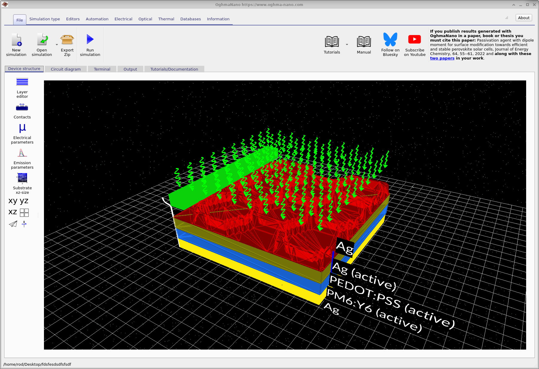
Once the circuit is built, OghmaNano scans the structure to compute the effective resistance to the extraction contact. The resulting maps highlight performance directly: low resistance near contacts and metal, and higher losses in poorly connected or central regions. This enables a clear design workflow: high resistance in cell centres points to mesh size, losses near contacts suggest extraction issues, and uniformly high resistance indicates poor conductor properties. The model shows where the design fails, not just how much. The same approach extends to illuminated devices, combining current spreading with diode behaviour and optics, as shown in the large-area PM6:Y6 tutorial.
5. From contact models to full illuminated devices
OghmaNano does not stop at resistive contacts. The same large-area framework can be extended to full devices by embedding diode elements into the network and supplying optical generation from a thin-film optical solver. In this case, lateral current collection is still handled by the 3D circuit model, but the local photovoltaic behaviour is captured through an illuminated diode equation. This is especially useful for large-area OPV and related thin-film device architectures, where current spreading and contact losses dominate at scale.
This allows you to bridge three levels of modelling within one environment:
- Contact-only models for current collection and sheet-resistance design.
- Large-area illuminated cells where diode behaviour and photogeneration are added.
- Complex 3D modules where current collection, geometry, and interconnection all matter simultaneously.
For related workflows, see: OPV simulation, OLED simulation, large-area PM6:Y6 solar-cell simulation, and complex 3D device and module structures.
6. Typical applications
This simulation framework is useful wherever current must spread laterally through a resistive layer before it reaches a highly conducting extraction contact. Typical applications include:
- large-area organic and perovskite solar cells,
- printed and flexible photovoltaics,
- OLED lighting panels,
- electrochromic and sensor devices,
- transparent electrode and mesh optimisation,
- module-level studies of contact design and shading.
In all of these cases, the central question is the same: how does geometry translate into electrical loss? OghmaNano answers that question directly by linking the 3D structure to a solved electrical network.