OghmaNano contains an advanced optical mode solver for calculating guided eigenmodes in one-dimensional slab waveguides, two-dimensional dielectric waveguides, and more complex cross-sectional optical structures. The solver is designed for problems in integrated photonics, slab waveguides, dielectric guides, fibers, and structured optical cross-sections. Rather than propagating light through time, the mode solver finds the stationary field distributions that can exist within a given refractive-index profile, together with their associated propagation constants and effective refractive indices.
The same mode-solving framework can be applied to 1D slab waveguides, 2D slab and box waveguides, and 2D complex waveguide cross-sections. Because the solver works directly with the transverse refractive-index distribution, it is particularly useful for studying modal confinement, polarization dependence, cutoff behaviour, and field patterns in structures that guide light by refractive-index contrast.
The user can define the refractive-index profile through the layer editor or by using free objects in the three-dimensional scene, then configure the solver from the Mode Calculator. In practice this makes it possible to move from a simple teaching example to a realistic integrated-photonics or fiber-style cross-section while staying within the same workflow and solver environment.
The optical mode solver finds guided solutions of Maxwell’s equations in the transverse plane. For a scalar transverse-electric formulation, the governing equation can be written as
\[ \nabla_{\perp}^{2} E + \left(k_{0}^{2} n^{2} - \beta^{2}\right)E = 0 \]
while for the transverse-magnetic formulation the solver uses
\[ \nabla_{\perp}\!\cdot\!\left(\frac{1}{n^{2}} \nabla_{\perp} H\right) + \left(k_{0}^{2} - \frac{\beta^{2}}{n^{2}}\right)H = 0 \]
Here \( \nabla_{\perp} \) acts in the plane transverse to propagation, \(n(x,y)\) is the refractive-index distribution, \(k_0\) is the free-space wavenumber, and \( \beta \) is the propagation constant of the mode. Solving this eigenvalue problem yields both the field profile and the effective index \(n_{\mathrm{eff}}=\beta/k_0\).
This is what makes the mode solver useful for guided-wave optics: instead of simulating a transient, it directly finds the optical states supported by a structure. From these solutions, one can determine whether a mode is guided or weakly confined, whether it is TE- or TM-like, and how confinement changes with geometry or wavelength.
The solver supports both transverse electric (TE) and transverse magnetic (TM) formulations. In slab and dielectric waveguides, these two polarizations behave differently at interfaces because the relevant field-continuity conditions are different. As a result, TE and TM modes may have slightly different effective indices, confinement strengths, and interface behaviour, even in the same structure.
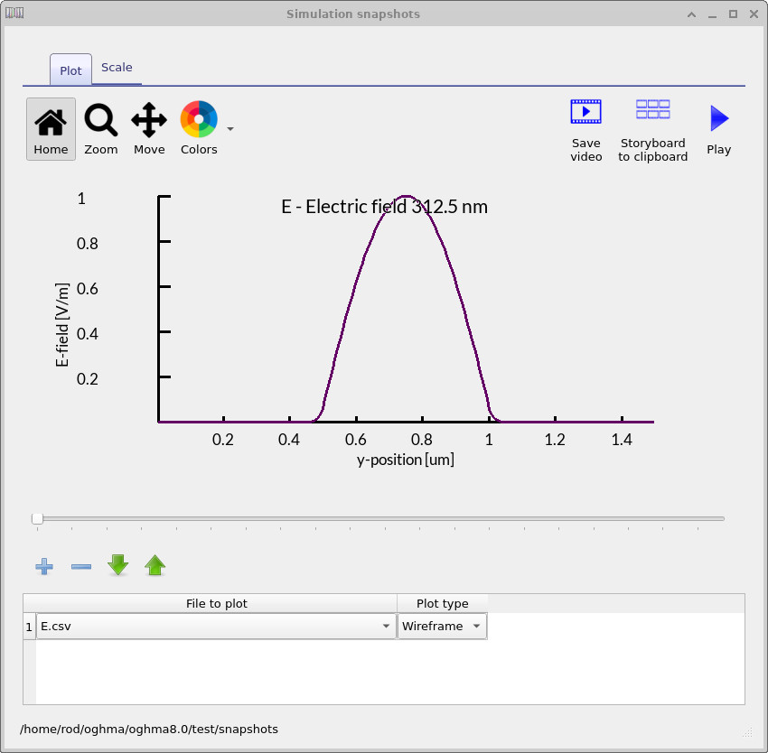
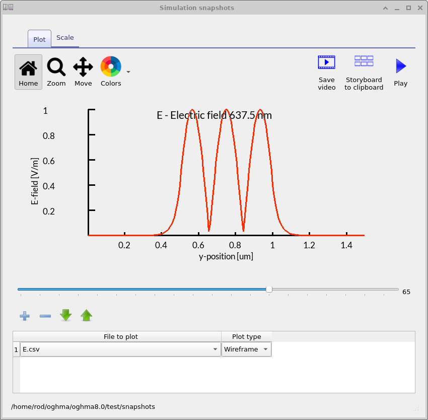
In a simple slab guide, the lowest-order mode is typically the most strongly confined and has no internal node across the core, as illustrated in Figure ??. As wavelength or core thickness changes, higher-order modes may appear, showing multiple lobes across the guide, as in Figure ??. These higher-order solutions are especially useful when teaching mode cutoff and understanding how confinement evolves in optical guides.
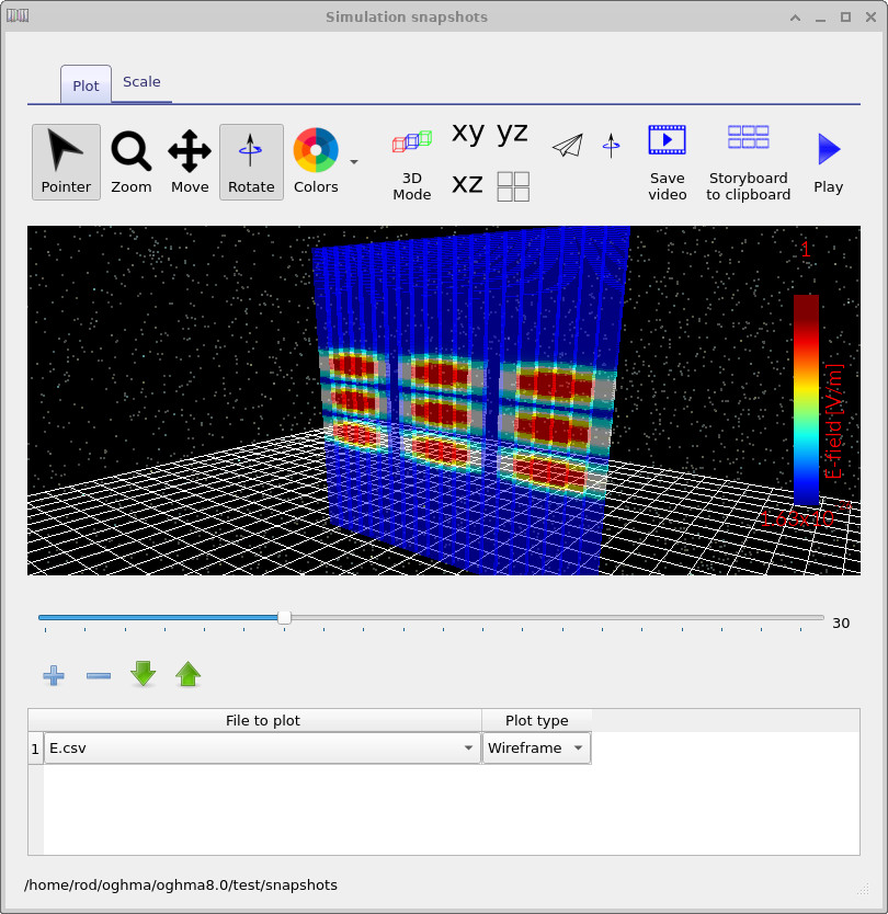
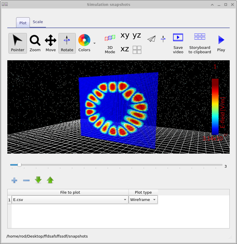
In two dimensions, the same ideas extend to waveguides with confinement in both transverse directions. This allows the solver to treat more realistic photonic structures, including box-like dielectric guides and non-trivial cross-sections where the field may become asymmetric or distorted by geometry. Examples are shown in Figure ?? and Figure ??.
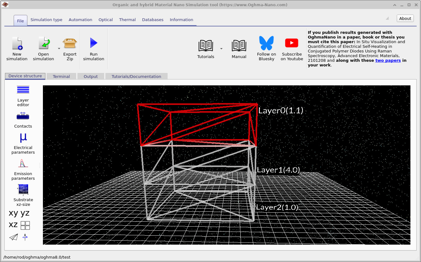
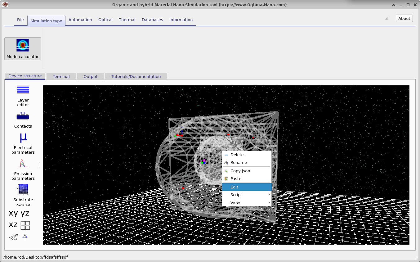
The mode solver fits naturally into the wider OghmaNano optical workflow. Simple slab structures can be defined in the layer editor, where the refractive index and thickness of each layer determine whether light can be confined. More complicated two-dimensional structures can be built from objects placed in the scene, making it possible to model fiber-like guides, off-centre inclusions, and other non-layered geometries.
Once the geometry is defined, the user configures the solver from the Mode Calculator. This is where polarization, wavelength range, solver tolerances, and eigenmode search settings are specified. The resulting field profiles are written to the output directory and explored through the snapshot viewer, where different modes can be stepped through interactively. This makes the solver useful not only as a design tool, but also as a visual teaching tool for understanding guided-wave physics.
Because the refractive-index distribution may vary strongly in space, mesh quality remains important. A sufficiently fine optical mesh is needed to resolve high-index contrast interfaces, narrow cores, and sharp field gradients. In practice, the mode solver therefore acts as both a numerical tool for calculating \(n_{\mathrm{eff}}\) and a diagnostic tool for checking whether the optical structure supports the intended modal pattern.
The optical mode solver can be used for a broad range of guided-wave problems. In its simplest form, it is ideal for studying slab-waveguide physics, including TE/TM polarization behaviour, cutoff conditions, and the appearance of higher-order modes. This makes it useful both for introductory photonics teaching and for fast design checks in layered dielectric systems.
In two dimensions, the solver becomes useful for integrated photonic waveguides, dielectric guides, rib or box guides, and fiber-like structures. Because the full transverse field distribution is available, the user can inspect mode shape, field symmetry, confinement, and leakage directly. This is especially important when validating optical cross-sections before using them in wider photonic-device workflows.
The solver is also a practical bridge between geometry and simulation. Structures created in the main OghmaNano environment can be checked rapidly for modal support before being used in other optical calculations. In this sense, the mode solver is not just a teaching module: it is a practical part of the optical design toolchain.
OghmaNano includes a set of guided tutorials for the optical mode solver. These take the user from simple one-dimensional slab guides through to two-dimensional waveguides and more complex cross-sections. They are intended both as a quick start for new users and as a source of practical examples for photonics problems.
Useful starting points include the 1D slab-waveguide mode-solver tutorial, the 2D slab and box-waveguide tutorial, and the 2D complex-waveguide tutorial. Taken together, these show how the same solver can be used for TE/TM comparison, modal cutoff studies, transverse-field inspection, and more complex geometries defined by objects rather than layers.
Try a mode-solver example.
Start with the 1D slab-waveguide tutorial for a quick introduction, then move on to 2D slab guides and complex two-dimensional waveguides.
These examples show how to define structures, run the eigenmode search, and inspect the resulting field profiles directly in the snapshot viewer.