1. Why perform parameter optimization?
When optimising a device, an engineer or scientist is often interested in determining the optimum structure rather than simply exploring how a single parameter varies. As a simple example, a perovskite solar cell consists of multiple layers, each of which has a thickness that influences device performance. The question then becomes: what is the optimum thickness of each layer?
If the perovskite layer is made very thick, a large fraction of the incident light will be absorbed. However, the downside is that charge carriers must travel further to escape the device, increasing their residence time and, consequently, the probability of recombination. Conversely, if the layer is made very thin, carriers can be extracted more efficiently, but fewer photons are absorbed in the first place.
The situation is further complicated by optical interference effects. Light reflects multiple times at the interfaces within the device, setting up standing-wave patterns that strongly depend on the thicknesses of all layers. As a result, optimising a single layer in isolation is rarely sufficient; instead, several layer thicknesses must be optimised simultaneously.
To address this type of multi-parameter optimisation problem, OghmaNano provides a Fast optimizer within the scan window, which can efficiently search the parameter space and identify favourable device configurations.
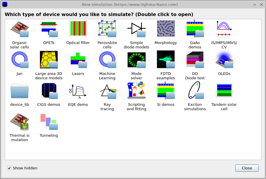
2. Opening the example
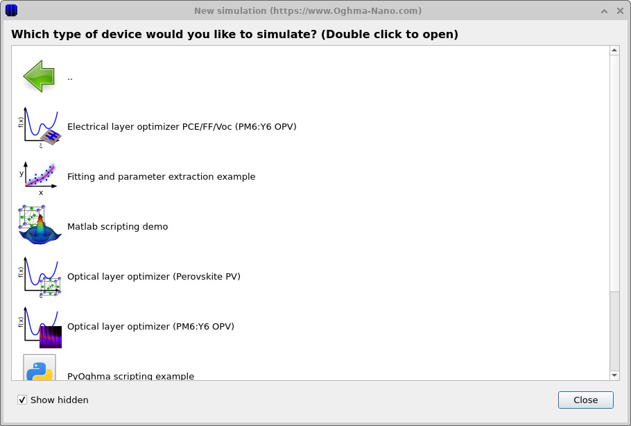
In the New simulation window, under the Scripting and fitting sub-topic, several examples demonstrate multi-parameter optimisation workflows:
- Electrical layer optimizer: Varies the thicknesses of two active layers in an organic solar cell and plots PCE, FF, and VOC as a function of layer thickness.
- Optical layer optimizer (Perovskite PV): Varies the thicknesses of two layers in a perovskite solar cell and plots the current generated in each layer.
- Optical layer optimizer (OPV): Varies the thicknesses of two layers in an OPV device and plots the current generated in each layer.
The example discussed on this page can be accessed via the New simulation button in the main window. This opens the New simulation browser shown in ??. From there, double-click Scripting and fitting to display the list of automation examples (??), then double-click Optical layer optimizer (Perovskite PV) to open the example referenced here.
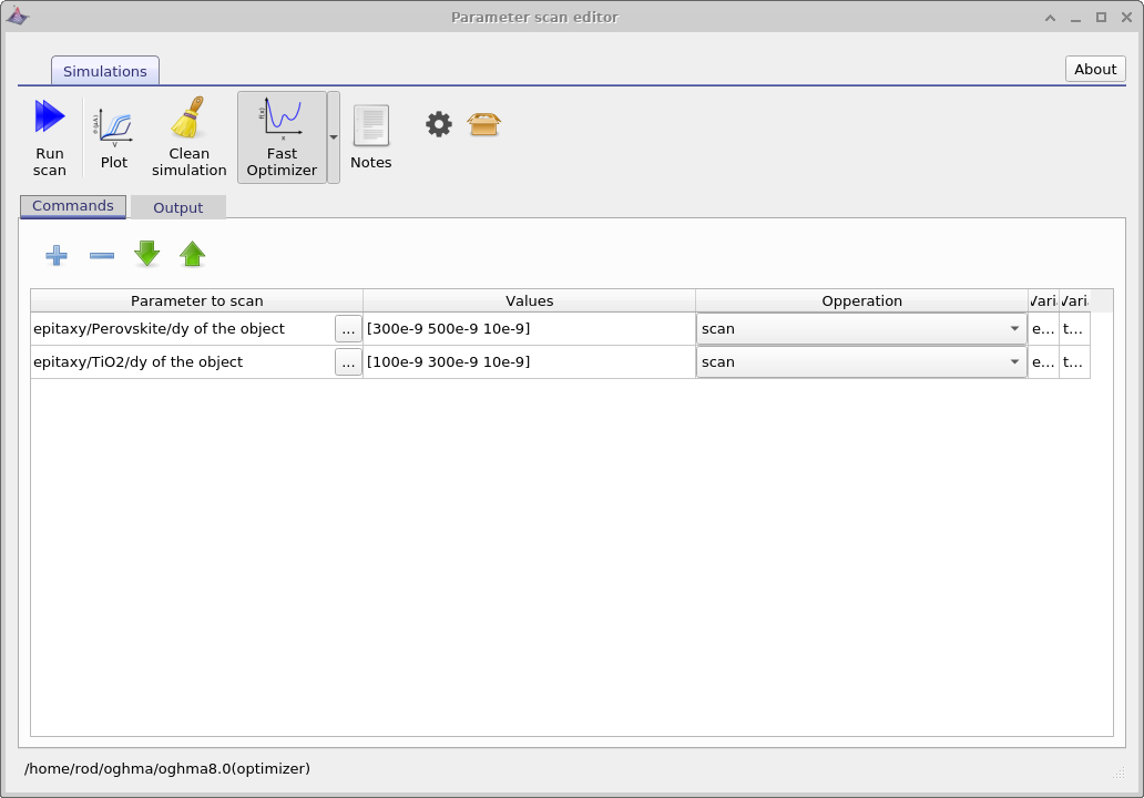
3. Using the multi parameter optimizer
Once the simulation has been opened, navigate to the scan tool, which can be found in the Automation ribbon. Clicking the Parameter scan icon reveals a scan that has already been configured, labelled optimizer. Opening this scan brings up the window shown in Figure ??.At first glance, this scan window looks identical to the scan windows described in the previous section. The key difference is that the Fast optimizer button is enabled. When this mode is active, individual scan results are not written to disk. Instead, the relevant simulation metrics are collected internally and written out in a single table at the end of the optimisation run.
In this example, the thickness (dy) of the perovskite layer is varied between 300 nm and 500 nm in steps of 10 nm, while the thickness (dy) of the TiO2 layer is varied from 100 nm to 300 nm, also in steps of 10 nm. Try running the simulation. Once it has finished, use your file manager to navigate to the simulation directory and open the folder named optimize. Inside this folder you will find a CSV file called optimizer_output.csv. Opening this file in Excel or LibreOffice produces a table similar to that shown in Figure ??.
If you examine figure 17.8 carefully you can see the first two columns are labelled epitaxy.layer2.dy and epitaxy.layer1.dy . These are the layer thicknesses we decided to change in the scan window. For every subsequent layer in the device there are two columns, labelled layerX/light_frac_photon_generation and layerX/J. These refer to the fraction of the light absorbed with in the layer and the maximum current this layer would produce if all the light absorbed within the layer were turned into current. Clearly if light is absorbed within the active layer it has a good chance of being turned into current, however if light is absorbed within the back metallic contact then there is little chance of that light being turned into electrical current. If you use the sorting tools included within Excel/LibreOffice you can figure out which device structures produce the most current.
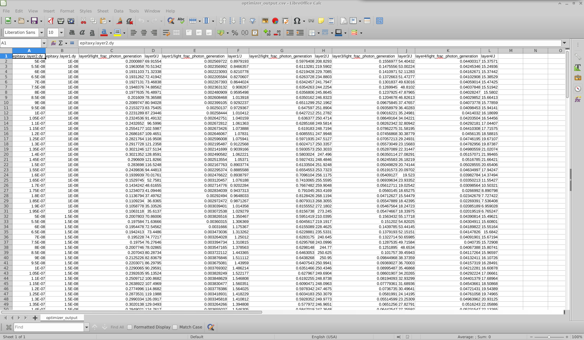
optimizer_output.csv file opened in LibreOffice Calc, showing layer thickness parameters alongside calculated outputs such as current density and photon generation for each layer.