Exciton Simulation Tutorial
1. Introduction
In this tutorial we will investigate how to simulate exciton dynamics in organic photovoltaic (OPV) devices. When a photon is absorbed in an organic semiconductor, it generates a bound electron–hole pair known as an exciton. In OPV devices, these excitons must drift or diffuse to a donor–acceptor interface where they can dissociate into free charge carriers. This process can be modeled using an exciton dissociation equation, which describes both exciton transport and their eventual conversion into electrons and holes. In OghmaNano, these exciton dynamics are introduced on top of the standard drift–diffusion equations to capture the full photophysical picture. A more detailed discussion of when exciton modeling is required (and when it can be omitted) is provided in Excitons and geminate recombination.
2. Getting started
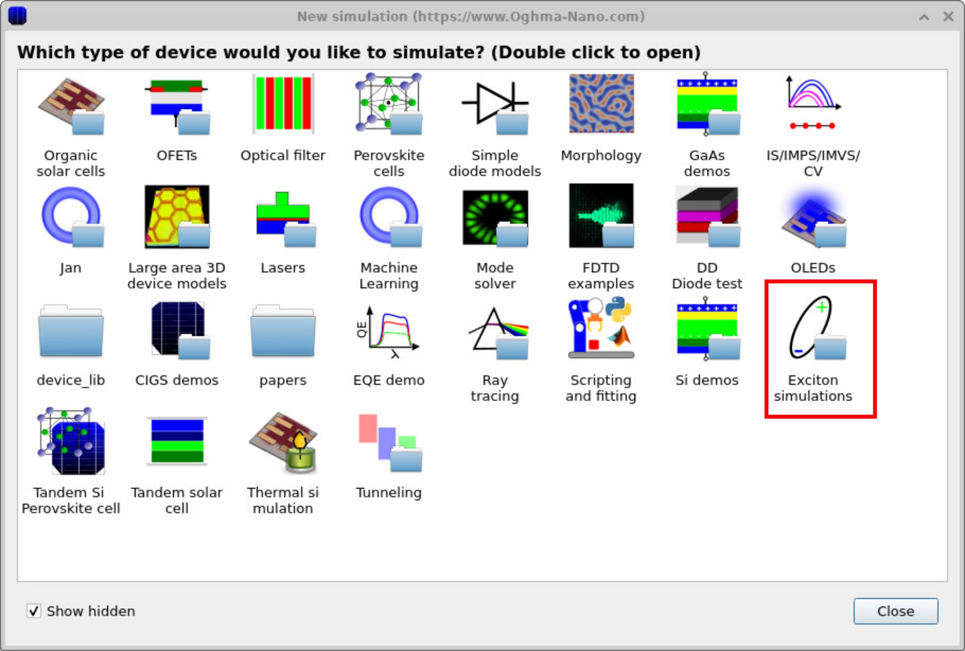
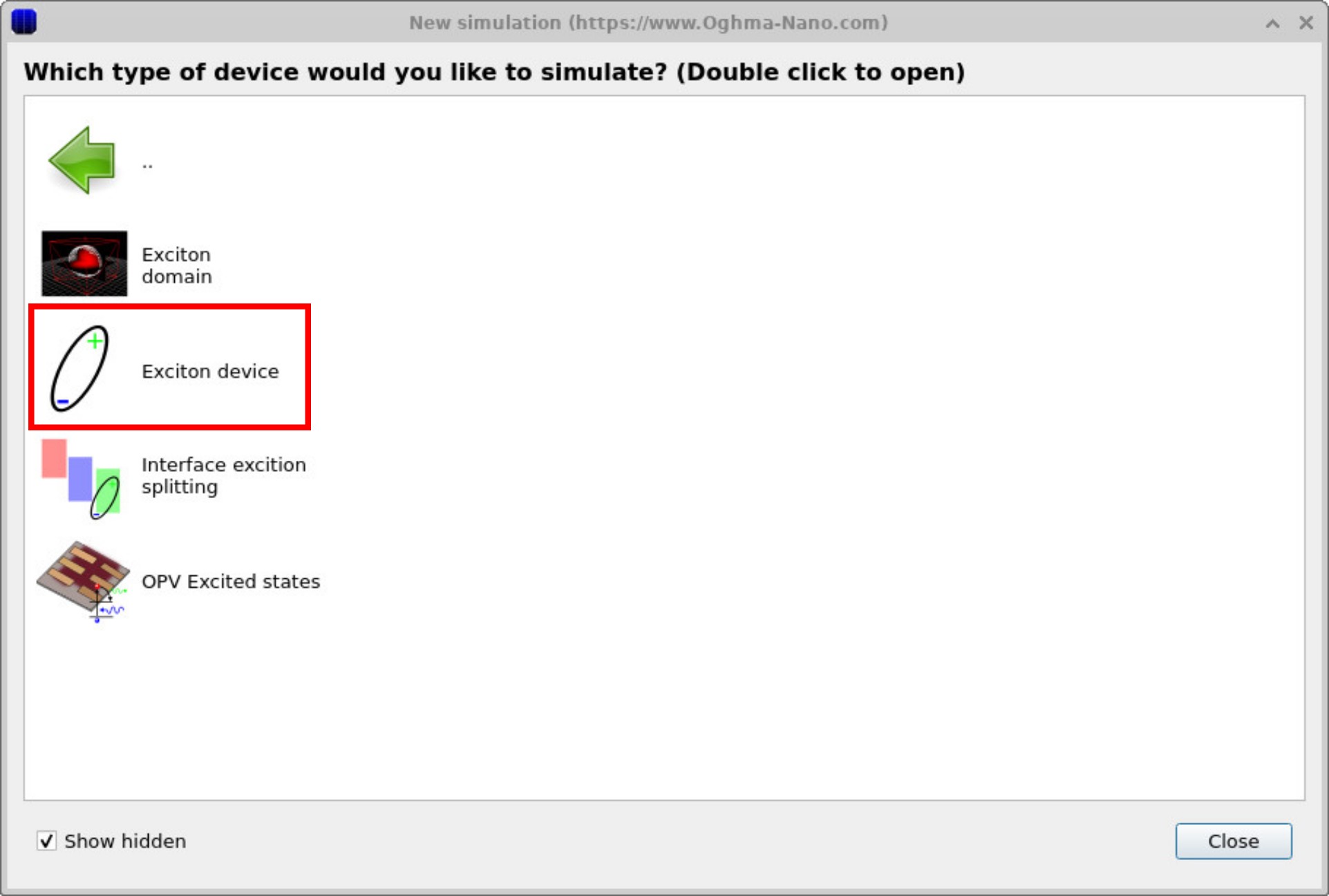
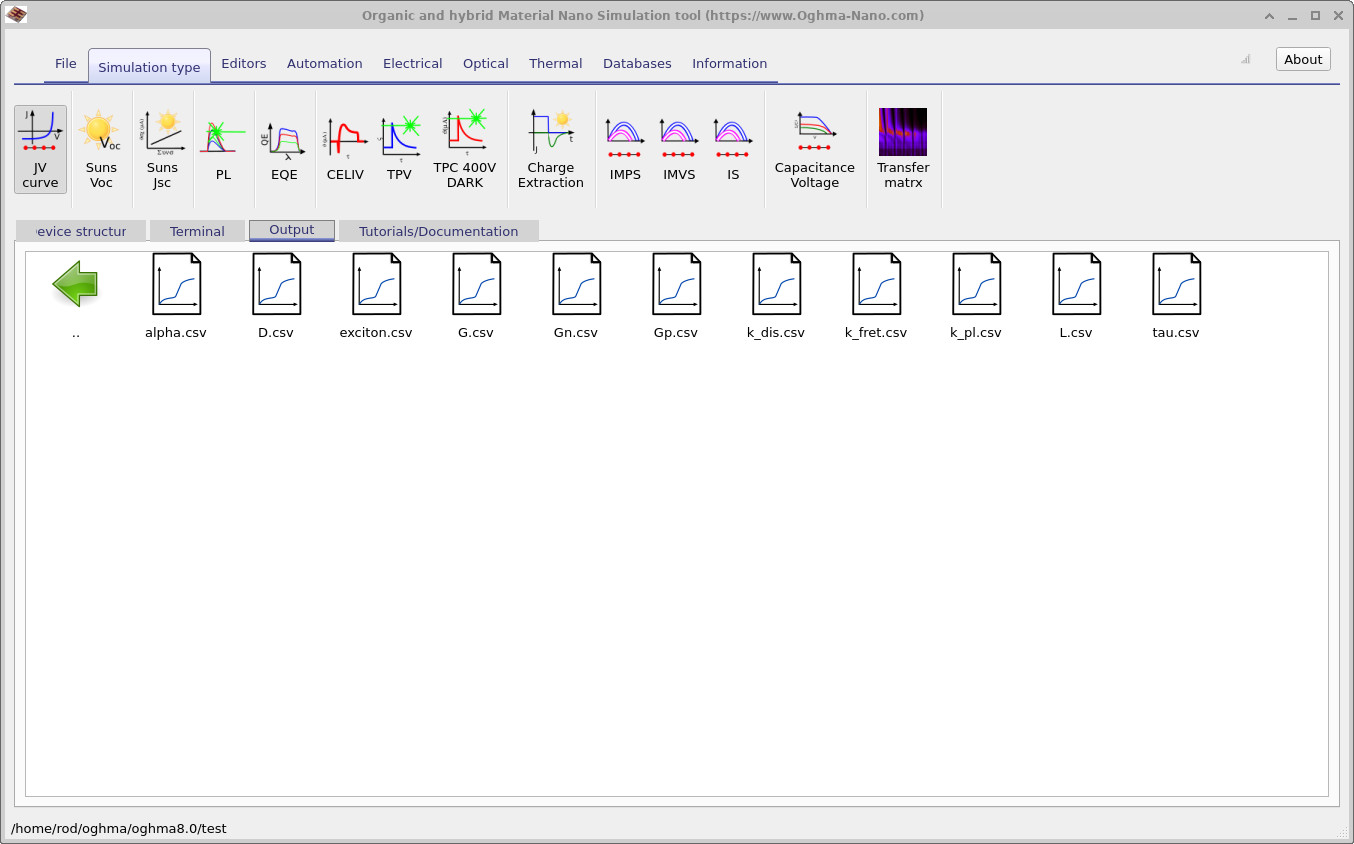
From the New simulation tab in the file ribbon, click to open the New simulation window (see Figure 1a). In this window you will find many categories of preconfigured examples. Double-click on the Exciton simulations folder to open the submenu of available exciton-related examples (see Figure 1b). For this tutorial we will use the Exciton device template, which provides a simple starting point for simulating exciton generation, transport, and dissociation in OPV structures.
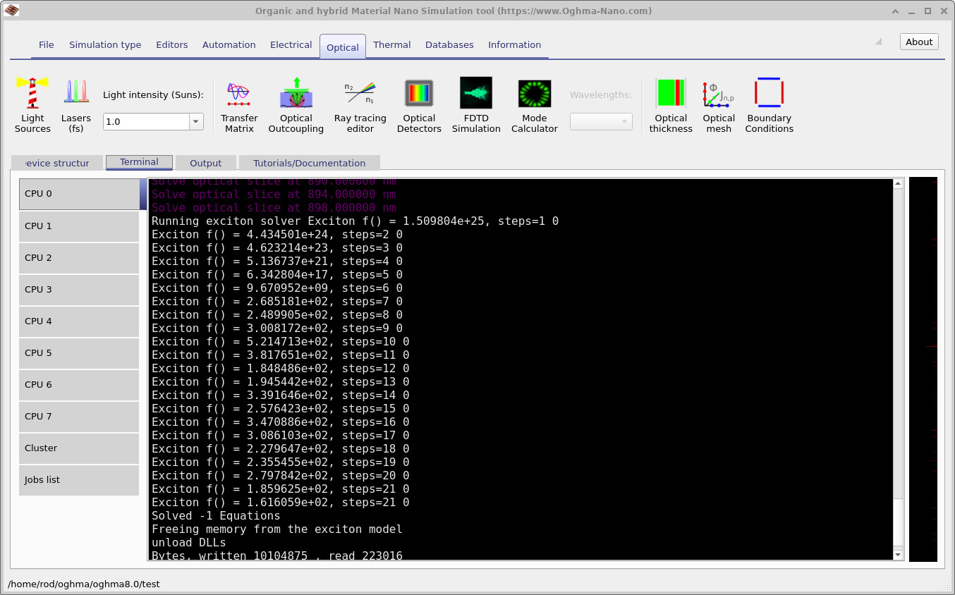
3. Run the simulation & inspect exciton outputs
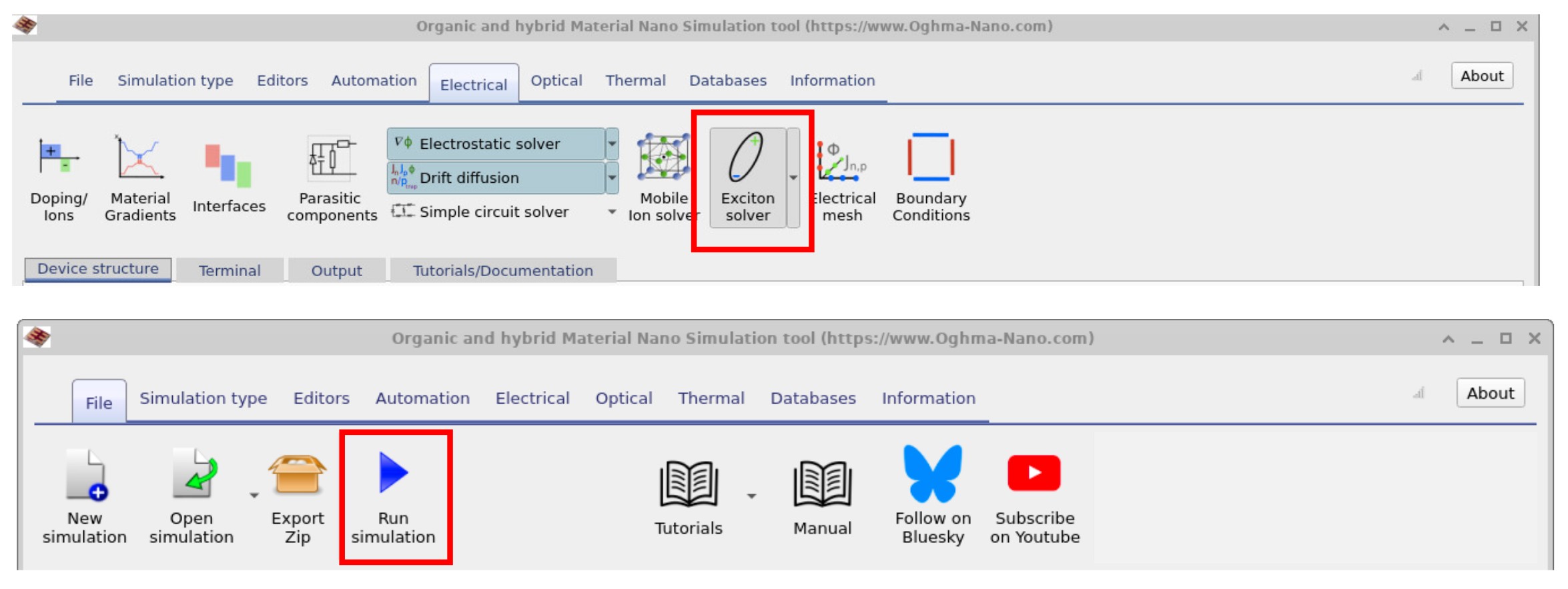
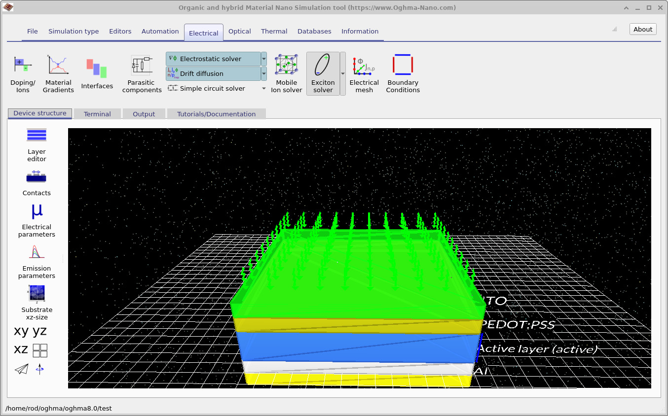
Once the device is opened, you will be able to see the stack in the main window. Before running the simulation, go to the Electrical tab and check that the Exciton solver button is depressed — it usually is by default, but it’s worth confirming (??). This ensures that exciton dynamics are enabled in the model. Once this is done, return to the File menu and press the Run simulation button to execute the model (??).
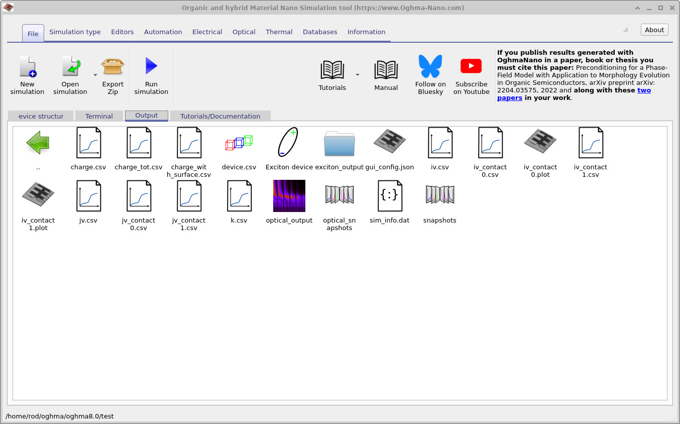
Once the simulation has finished, you can inspect the results in the
Output tab (??).
This lists all of the files written to disk, including exciton-related outputs.
By double-clicking on jv.csv, you can plot the JV curve
(??).
The plot looks like a standard JV curve you would obtain from any device simulation,
but in this case the Exciton solver was enabled, meaning exciton dynamics
are included in the underlying physics.
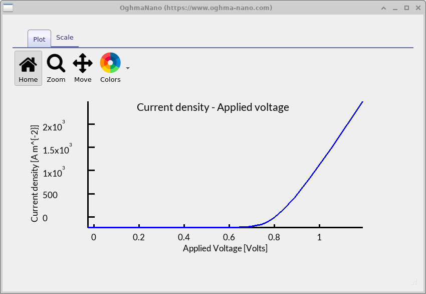
jv.csv.
Although it looks like a standard JV curve, the Exciton solver is enabled.
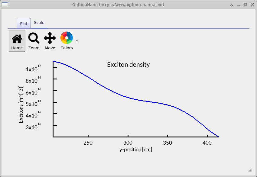
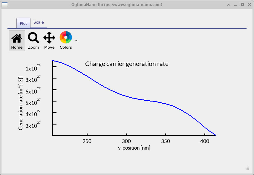
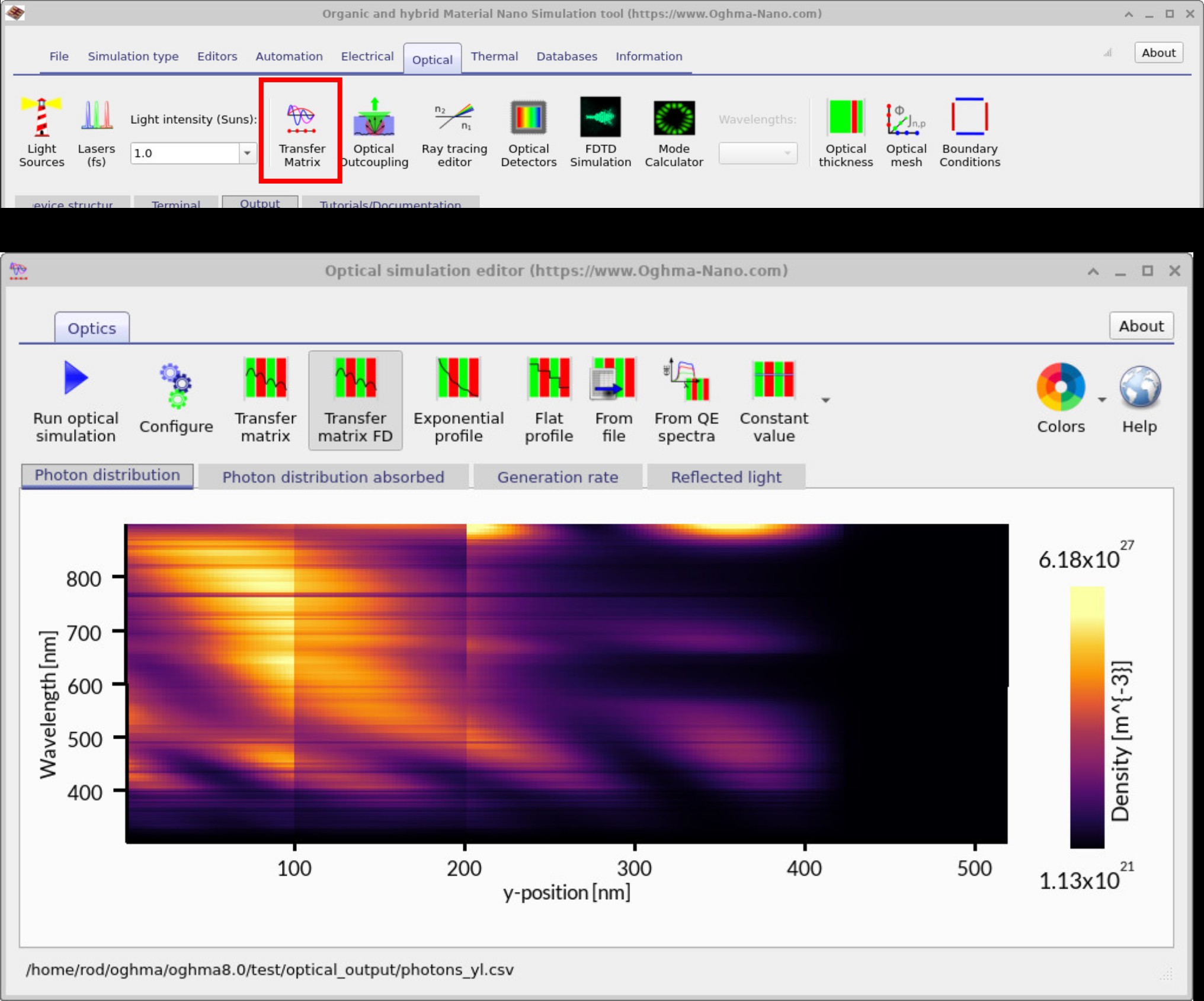
If you double-click on the exciton_output folder within the output directory, you can access the detailed results of the exciton solver (see ??). This directory contains all solver outputs, including constants as a function of position and calculated quantities derived from the exciton dynamics. For example, double-clicking on exciton.csv produces a plot of the exciton distribution across the device thickness (see ??). Similarly, Gn.csv gives the electron generation rate as a function of position, while Gp.csv shows the hole generation rate (see ??). In the case of a simple 1D device, these two generation rate files are effectively identical.
exciton_output folder in the simulation output directory.
4. Exciton transport equation and parameters
The exciton distribution within the device is governed by the exciton transport equation:
\[ \frac{\partial X}{\partial t} = \nabla \!\cdot \!\big(D\,\nabla X\big) + G_{\mathrm{optical}} - k_{\mathrm{dis}}\,X - k_{\mathrm{FRET}}\,X - k_{\mathrm{PL}}\,X - \alpha\,X^{2} \]
Here \(X(\mathbf{r},t)\) is the exciton density (m\(^{-3}\)); \(D\) is the exciton diffusion coefficient (m\(^2\)s\(^{-1}\)); \(G_{\mathrm{optical}}\) is the local exciton generation rate supplied by the optical model (proportional to absorbed photons); \(k_{\mathrm{dis}}\) is the dissociation rate to free charges; \(k_{\mathrm{FRET}}\) is the Förster resonance energy transfer rate; \(k_{\mathrm{PL}}\) is the radiative decay rate; and \(\alpha\) is the exciton–exciton annihilation coefficient (m\(^3\)s\(^{-1}\)). When this model is enabled, the electronic drift–diffusion equations use a generation term defined as \(G = k_{\mathrm{dis}}\,X\), optionally restricted to interfacial regions if configured.
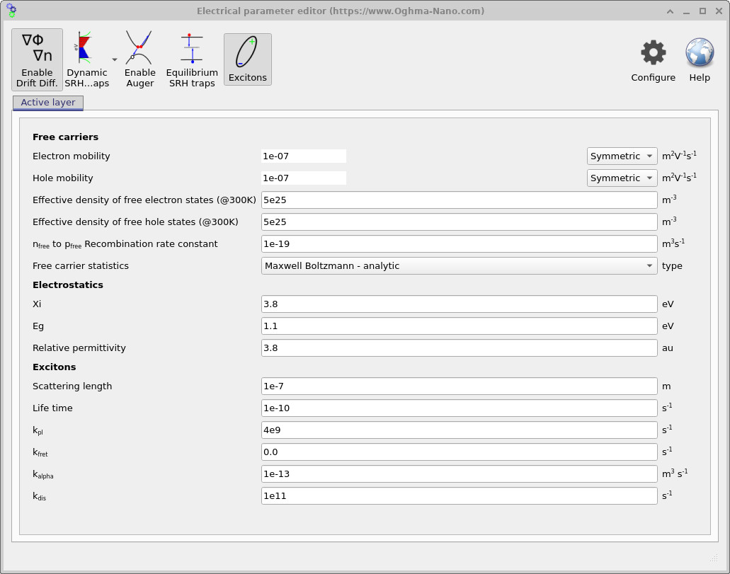
All of these parameters can be viewed and modified in the Electrical parameter editor, accessible from the main menu (see ??). The exciton-specific fields are grouped under the Excitons heading. These are summarised in the table below.
| Parameter | Meaning | Units |
|---|---|---|
| Scattering length | Effective diffusion length of excitons before scattering. | m |
| Lifetime | Average time an exciton survives before decay or dissociation. | s |
| kPL | Radiative decay rate (photoluminescence). | s⁻¹ |
| kFRET | Förster resonant energy-transfer rate. | s⁻¹ |
| kα | Exciton–exciton annihilation coefficient. | m³ s⁻¹ |
| kdis | Dissociation rate constant, converting excitons into free charges. | s⁻¹ |
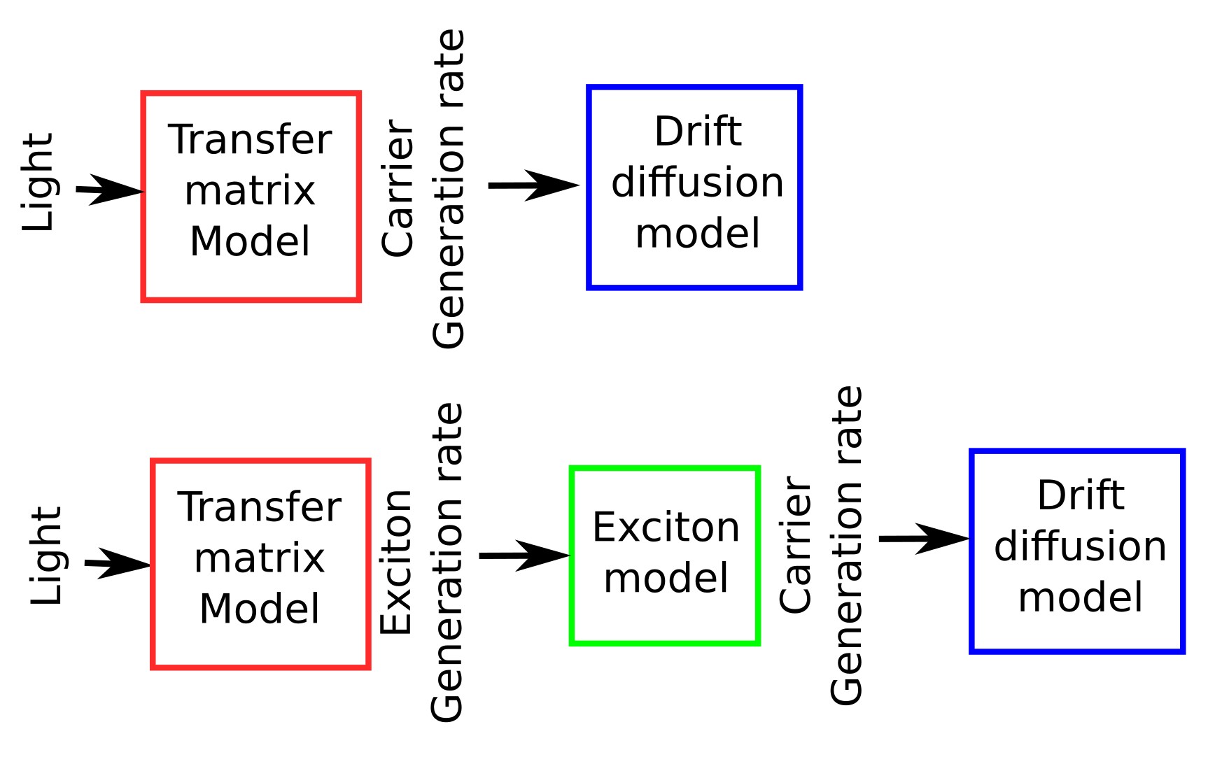
5. How the solver fits in with the simulation process
When the exciton solver is turned off (top of ??), the transfer-matrix optics computes the carrier generation rate and passes it straight to the drift–diffusion solver. When the exciton solver is on (bottom of ??), the optics instead provide an exciton generation rate to the exciton solver. The exciton solver then evolves that population—diffusing, transferring (FRET), dissociating, radiatively decaying, and annihilating—using the parameters set in the Electrical parameter editor, and outputs the final carrier generation rate for the drift–diffusion solver. In short, the exciton solver inserts itself between optics and electrical transport so you can model exciton physics without changing the optical setup or the drift–diffusion equations.
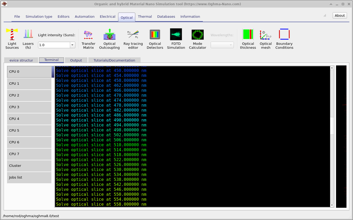
The sequence of operations in the exciton-enabled simulation is illustrated in ??. First, the optical solver is executed, computing the photon absorption profile slice by slice across the device. Next, the exciton solver runs, where the generated excitons are propagated, transferred, or dissociated until the solver converges, typically within a few tens of steps. Finally, the exciton generation rate is examined as a function of both device depth and wavelength, as calculated by the transfer matrix model. Together, these outputs form the pipeline that links the optical model to the exciton solver, and ultimately to the drift–diffusion equations.
💡 Tasks: Try these simple edits to explore the exciton model (Hint, change them by one to two orders of magnitude to see an effect.):
- Change the exciton lifetime in the Electrical parameter editor and rerun the simulation.
- Reduce the dissociation rate (kdis) and observe its effect on carrier generation.
- Increase the exciton–exciton annihilation coefficient (α) to simulate stronger exciton–exciton interactions.
- Compare the JV curve with the exciton solver enabled vs. disabled.
✅ Expected results
- Longer exciton lifetimes lead to higher exciton densities and increased carrier generation.
- Lower dissociation rates reduce the photocurrent since fewer excitons are converted into free carriers.
- High annihilation rates broaden or suppress the exciton density profile, lowering efficiency.
- JV curves with the exciton solver enabled may show reduced JSC compared to the standard drift–diffusion model, especially if trapping or annihilation is significant.
📘 Return to the introduction to organic electronics for a broader overview of the topic.