Simple circuit simulations
1. Introduction
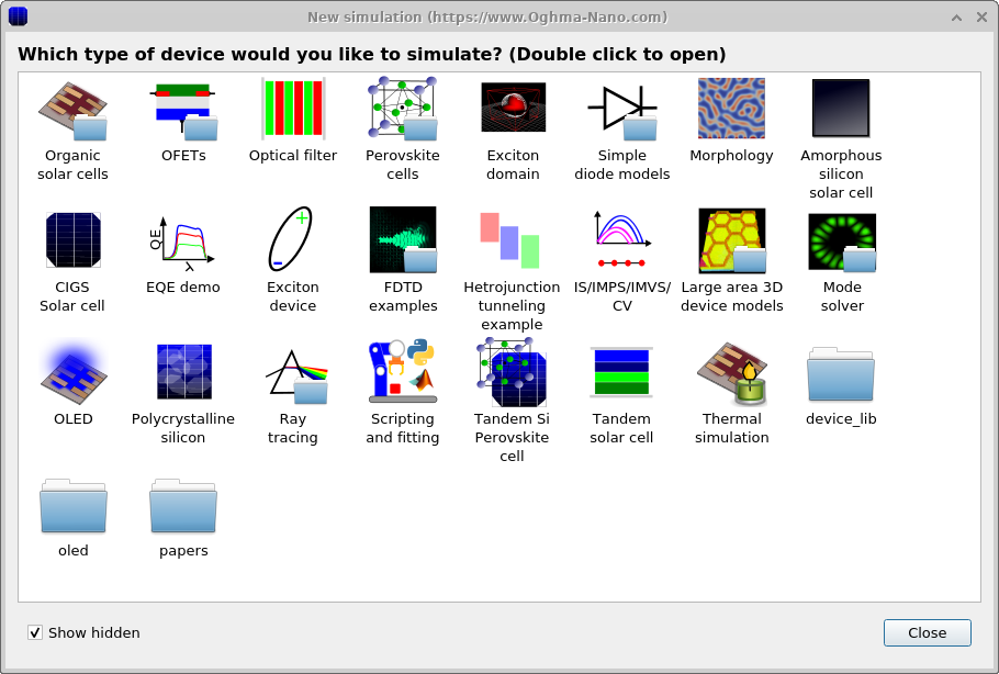
Although full drift–diffusion simulations are a powerful way to analyze device behavior in detail—capturing effects such as recombination rates, carrier mobilities, and other microscopic processes—they are also inherently complex to run and interpret. They require many material parameters, which are often unavailable, and in many cases such fine-grained detail is not necessary. Sometimes you simply want to diagnose a shunt path, assess series resistance, or gain a quick understanding of overall device behavior. In such situations, it is often more practical to use simplified electrical models. A simple equivalent circuit consisting of resistors, capacitors, and ideal diodes is often sufficient. To support this, OghmaNano provides a built-in circuit solver, similar in spirit to LTspice, that allows you to apply arbitrary voltages to arbitrary circuit networks and obtain realistic electrical responses. This solver is a direct drop-in replacement for the drift–diffusion engine: applied voltages are defined in the same way, and all experimental modes—such as time domain, frequency domain, and EQE—remain compatible. In addition, the transfer matrix model used to calculate optical absorption can be coupled to the diodes, allowing photocurrent to be simulated consistently. Several example circuit simulations are included in the software and can be found in the Simple Diode Model folder of the new simulation window (see Figure 1).
In this tutorial, we will use the simple circuit solver to model a PM6:Y6 solar cell in a straightforward way and gain a basic understanding of its behavior.
2. Getting started
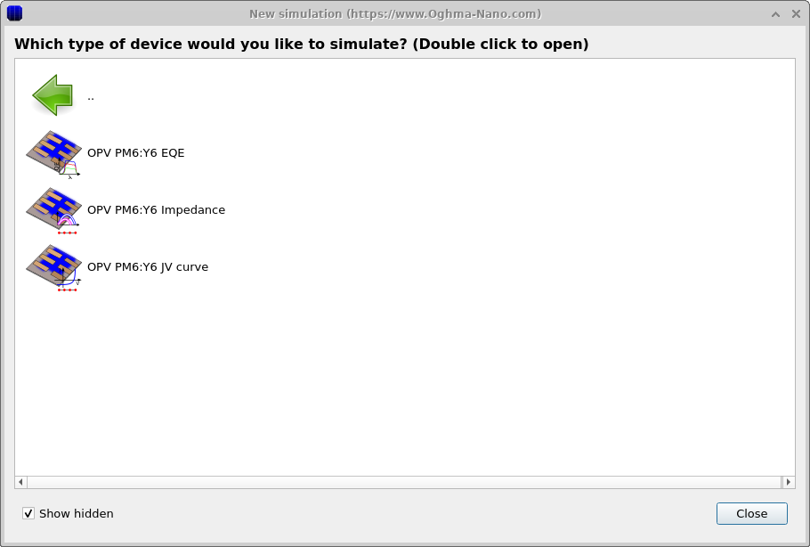
From the New simulation tab in the file ribbon, click to open the New simulation window (see Figure 1a). If you then double-click on Simple Diode Models, the software will display a submenu of available circuit examples (see Figure 1b). For this tutorial we will use the OPV PM6:Y6 JV curve example. We begin with the JV curve because it is the simplest circuit-based simulation to run.
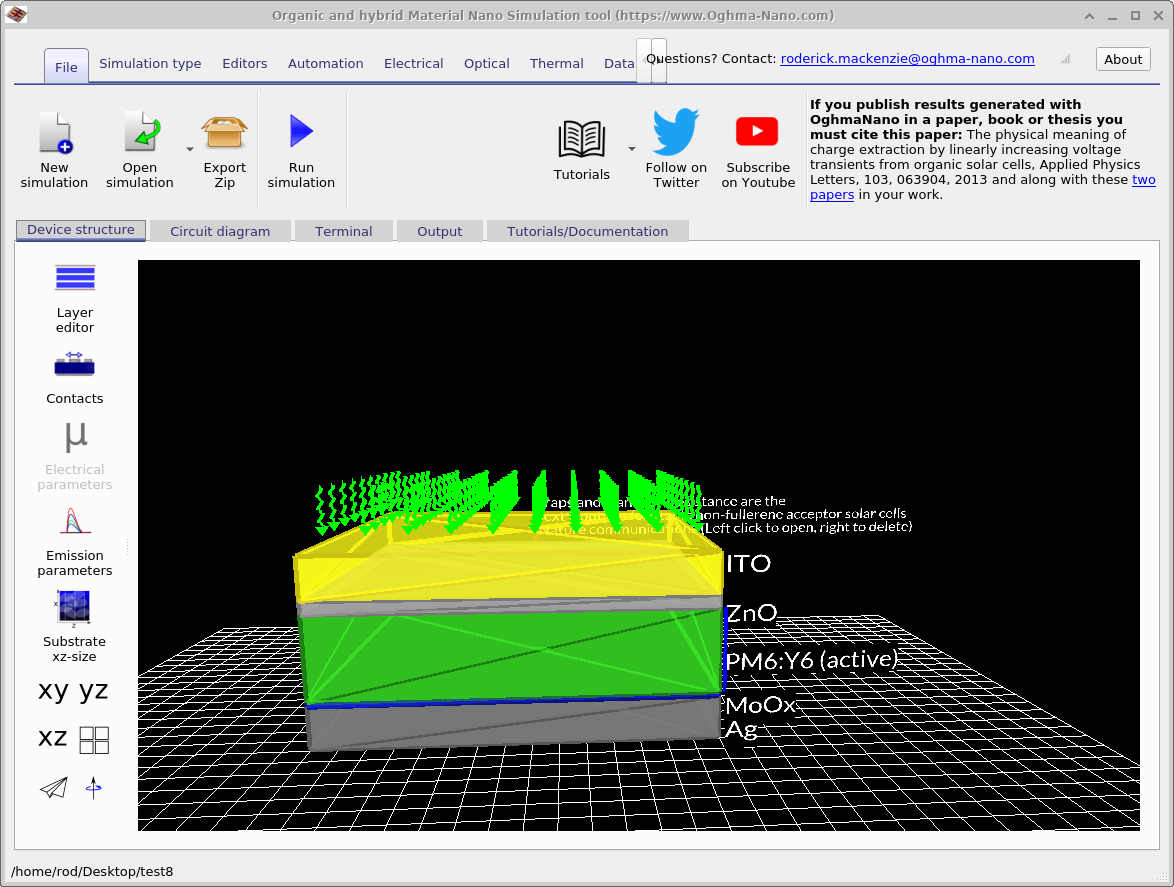
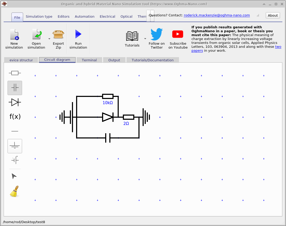
Once you have saved your new simulation, a window resembling the standard OghmaNano simulation interface will open. This is shown in Figure 3. It looks just like a normal simulation window, except that the Electrical Parameter Editor is greyed out. You will also notice that a second tab has appeared called Circuit Diagram. Clicking on this tab opens the circuit diagram editor, shown in Figure 4. Here the device is represented by a simple equivalent circuit consisting of a diode, a series resistance, a shunt resistance, and a capacitor. This provides the most basic solar cell model. The capacitor accounts for geometric capacitance from the contacts, which will be important later when we explore time- and frequency-domain simulations.
3. Editing the circuit
On the left-hand side of Figure 4 you can see a set of standard electrical components available in the circuit editor. These include a resistor, capacitor, diode, wire, ground, and battery. There are also two tools: a pointer for selecting and editing components, and a brush tool used for deleting them. Each button is described in more detail in the table below.
| Component/Tool | Equation | Description |
|---|---|---|
| Resistor | \(V = IR\) | Models ohmic resistance in the circuit. |
| Capacitor | \(I = C \tfrac{dV}{dt}\) | Stores and releases charge, representing geometric or parasitic capacitance. |
| Diode | \(i(t,V) = I_{0}\!\left(e^{\tfrac{qV}{nkT}} - 1\right) - I_{\text{light}}\) | Represents an ideal diode; \(I_{\text{light}}\) is taken from optical simulations. |
| Non-linear element | \(i(t,V) = \left(\tfrac{I_{0} \cdot V}{V_{0} + d}\right)^m\) | User-defined non-linear element for advanced circuit modelling. |
| Wire | — | Ideal wire with no parasitic parameters. |
| Earth | — | Ground reference set at 0 V. |
| Battery | — | Applies voltage to the circuit, taken from the contact marked change in the contact editor. |
| Pointer | — | Used to select and edit circuit elements. |
| Brush | — | Used to delete circuit elements. |
By clicking on any circuit element with any tool apart from the brush, you can change the values of the components as seen in [fig:circuit_edit_component], and zoomed in [fig:circuit_edit_component_zoom].
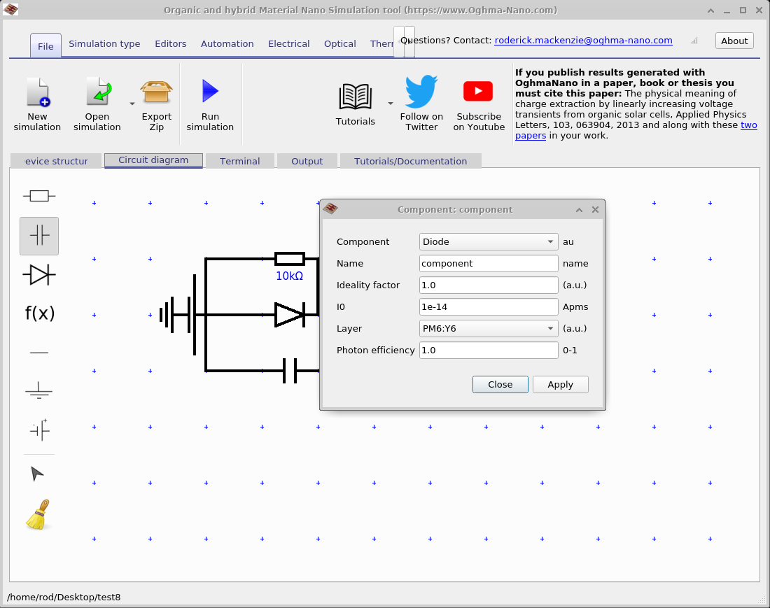
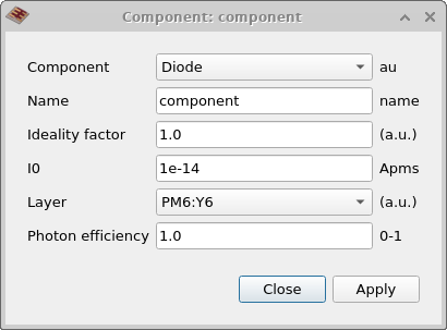
When you click on any component in the circuit editor, an edit box appears that allows you to change its parameters. Most of these settings are straightforward and easy to understand. The most detailed configuration appears for the diode model, which has several additional parameters. This edit box is shown in Figure 5, and the options are explained in the table below.
| Parameter | Description |
|---|---|
| Component | Selects what type of component the circuit element represents. |
| Name | Human-readable label for the component; you can choose any name. |
| Ideality factor | The diode ideality factor n. |
| I0 | Saturation current in the diode equation. |
| Layer | The layer the diode represents; the light current is calculated from generation in this layer. |
4. Running the circuit editor
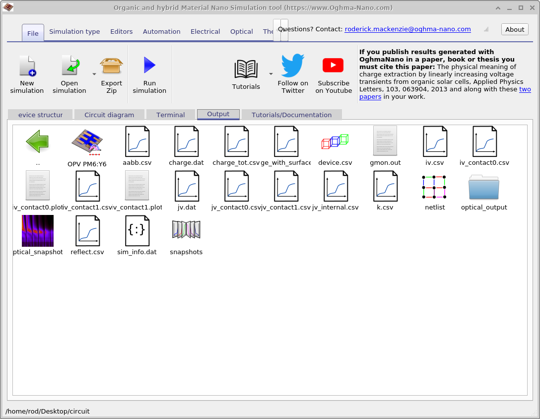
Go to the main simulation window, locate the Play button (▶), and click it — or simply press F9 — to run the simulation. Once started, OghmaNano first evaluates the selected optical model (e.g. Transfer Matrix or Ray Tracing) and then couples its output into the circuit solver to generate the device’s photocurrent. A JV sweep is then performed in exactly the same way as in full drift–diffusion simulations.
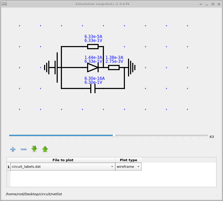
In addition to the standard output files, the circuit solver also produces a Net list. This is shown in
Figure 11.2. Double-clicking the
netlist file opens a window that displays the voltage across and current through every component in the
circuit. You can use the slider to step through each simulation point (time or voltage). Note that the net list is
only created if Write everything to disk is enabled in the simulation editor.
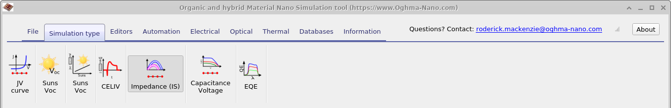
5. More advanced simulation types
real_imag.csv).
Up to this point we have performed a standard JV simulation, but because the circuit solver is fully integrated
with all the other tools in OghmaNano, you can also run a wide range of advanced analyses. By selecting
different modes from the Simulation types ribbon in the main menu, you can perform
Suns–VOC, Suns–JSC, C–LIV simulations,
Impedance Spectroscopy, Capacitance–Voltage, and EQE measurements.
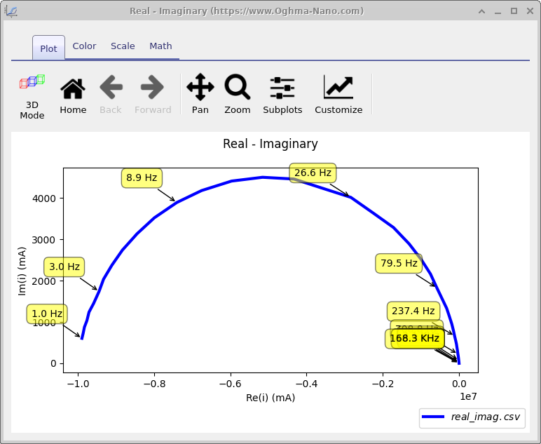
An example is shown in Figure 9,
where the real and imaginary components of the impedance response (real_imag.csv) are plotted for the
circuit model. All of these tools operate exactly as they do in full drift–diffusion simulations, but here they
carry the additional advantage of being coupled directly to the optical model at the same time.
6. Using the fitting/scan tools with circuit models
The circuit models are exposed in the json tree just like the drift diffusion material paramters and therefore you can also use the fitting and scan tools to either fit the data to experiment or to scan through circuit values.