SCLC Simulation Tutorial: Mott–Gurney Law and Mobility Extraction
Space-charge limited current (SCLC) is the transport regime where injected carriers dominate and the current is limited by their motion through the film, not by generation. In an ideal, trap-free device, the current density follows the Mott–Gurney law: \( J = \frac{9}{8}\,\varepsilon\,\mu\,\frac{V^2}{L^3} \), with dielectric constant \( \varepsilon \), mobility \( \mu \), voltage \( V \), and thickness \( L \). SCLC measurements (often using hole-only or electron-only diodes) are widely used to extract mobility and assess trap effects. In this quick start, you will configure an SCLC structure, run a JV sweep, locate the J ∝ V² region, and see how traps or thickness shift the curve and the extracted mobility.
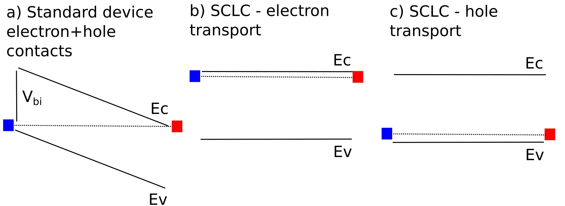
In ?? we compare contact configurations that control which carriers can enter the device. In panel (a) the standard structure has electron- and hole-selective contacts, creating a built-in potential and allowing both electrons and holes to be injected/extracted. By adjusting the contact energetics or adding/selecting transport/blocking layers, you can enforce single-carrier injection: in panel (b) an electron-only device (SCLC) is formed by providing low barriers to the conduction band at both contacts while blocking the valence band (hole injection), and in panel (c) a hole-only device (SCL) is formed by aligning the valence band at both contacts while blocking the conduction band (electron injection). Compared to the standard device in (a), the single-carrier cases (b,c) suppress recombination and force current to be governed by space-charge-limited transport, which is ideal for extracting carrier mobility and contact effects.
The derivation of the Mott–Gurney equation, together with a detailed discussion of the physical assumptions and limitations of SCLC theory - including trap-free transport, ohmic injection, negligible diffusion current, and single-carrier transport — can be found in the sections Derivation of the Mott–Gurney equation and Validity conditions of the Mott–Gurney equation.
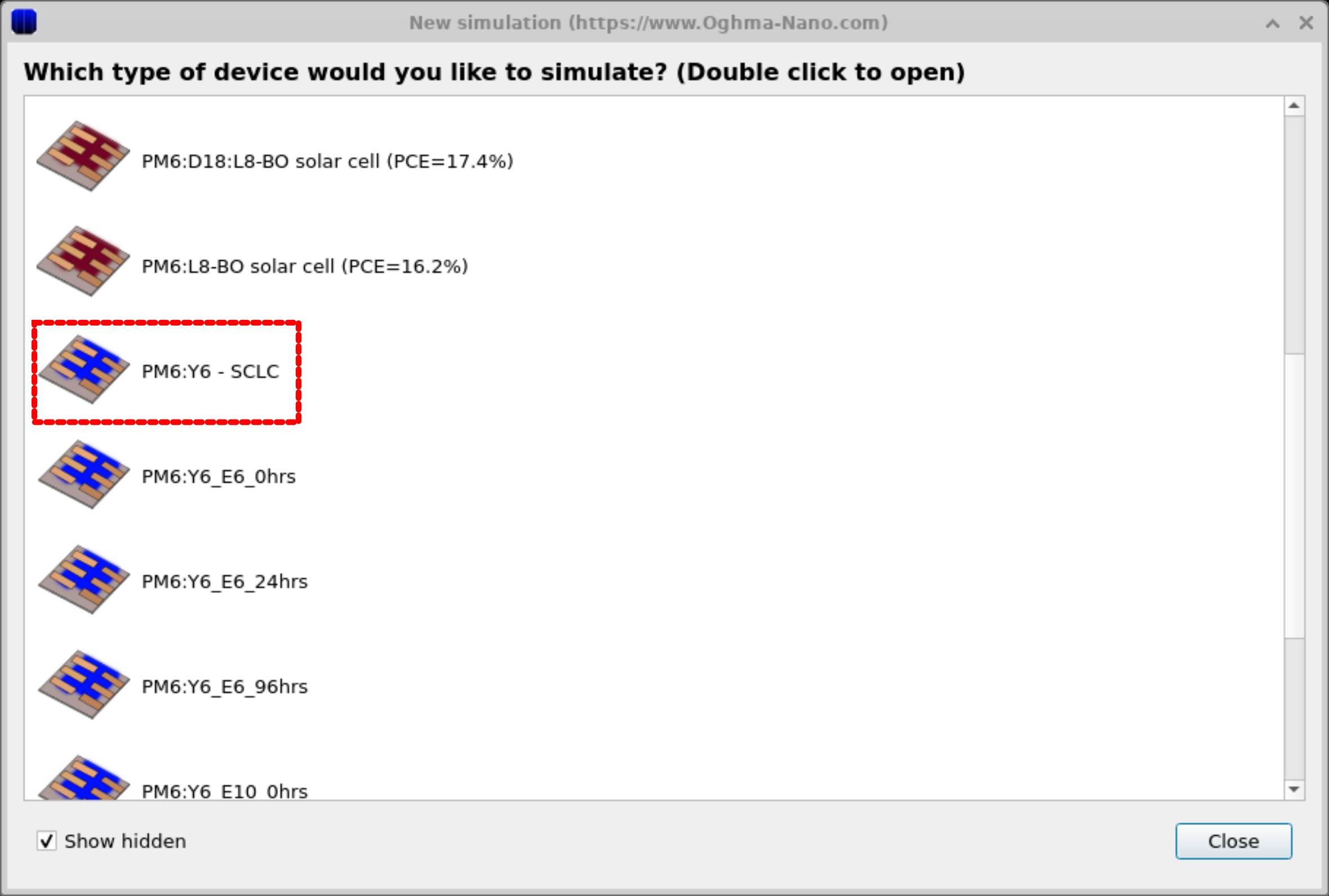
Step 1: Create a new SCLC simulation
Start OghmaNano from the Windows Start menu. The main OghmaNano window will appear as shown in ??.
Step 2: Check the contacts are set up for SCLC
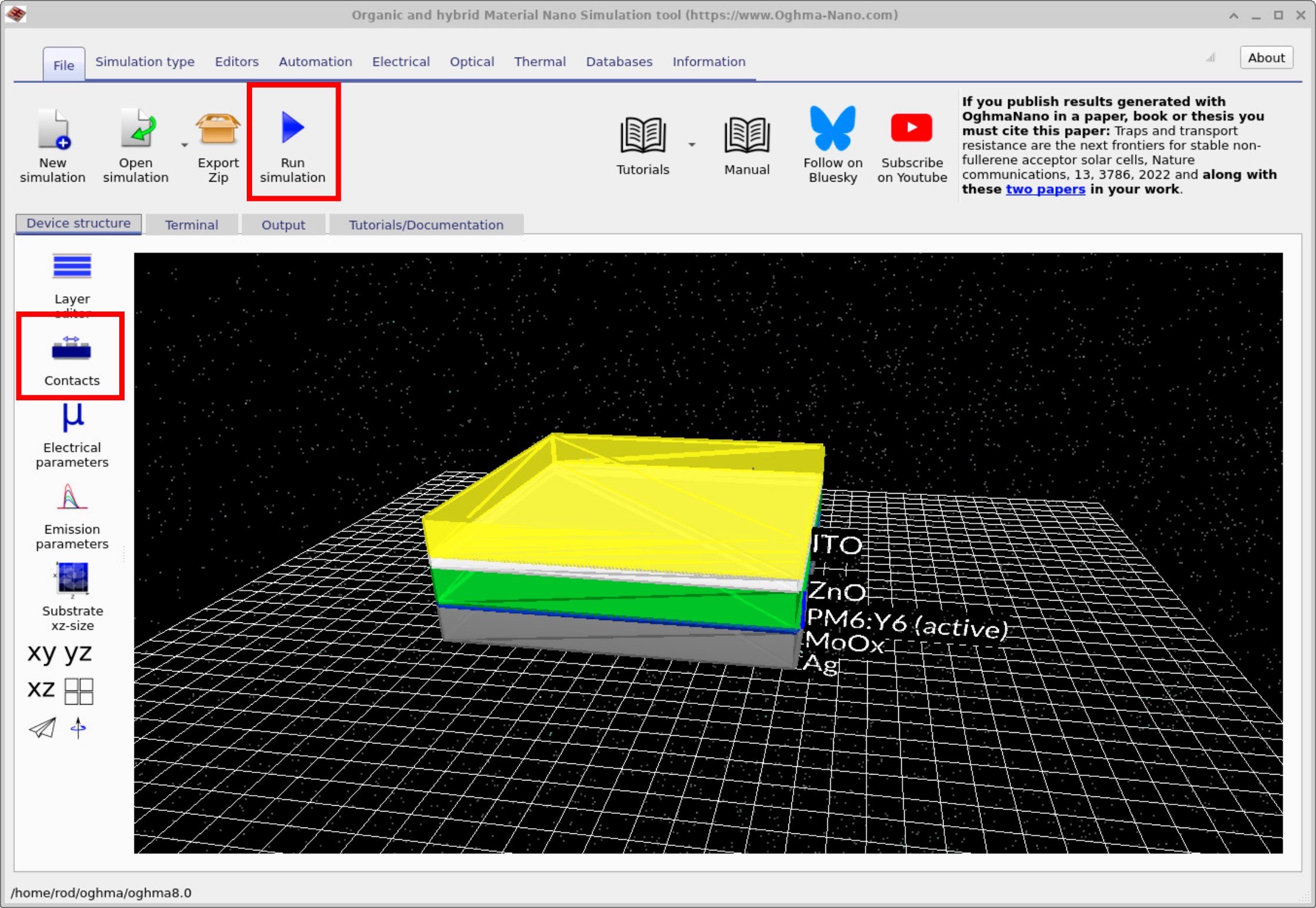
Once you have saved the SCLC example, the main window (??) will appear. This shows the 3D representation of the device. The two key buttons we will be using in this window are the Run Simulation button and the Contacts button.
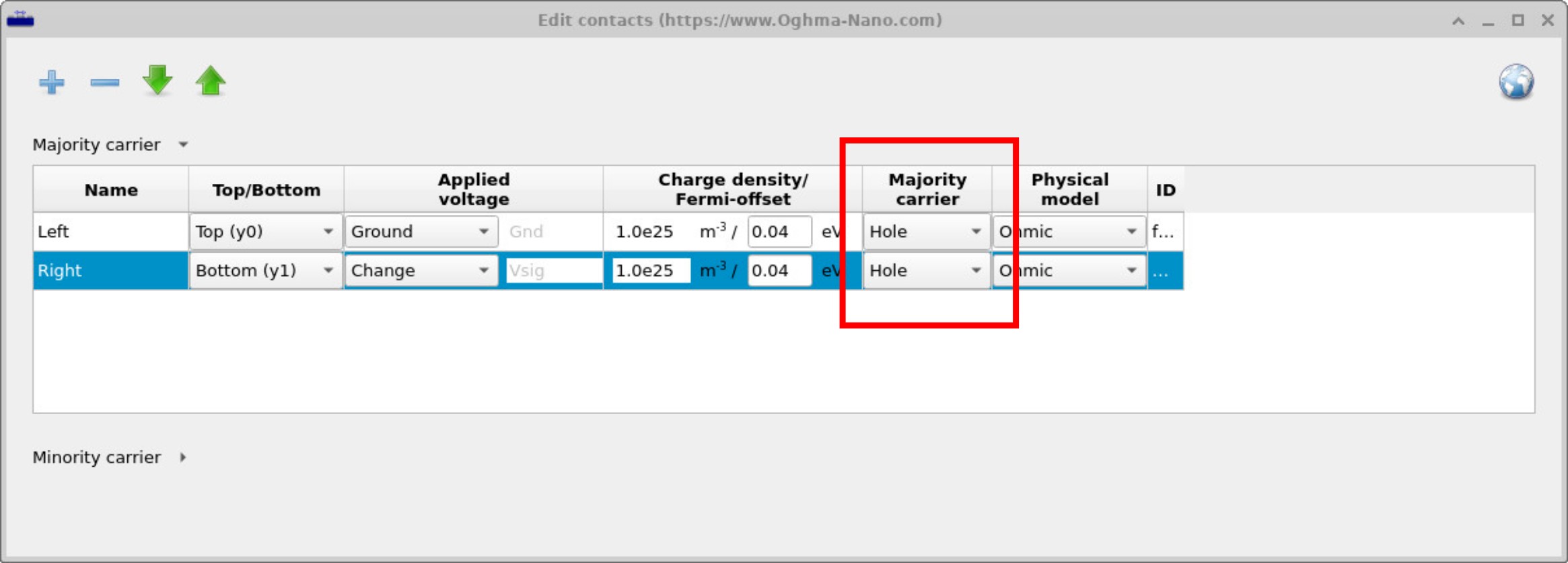
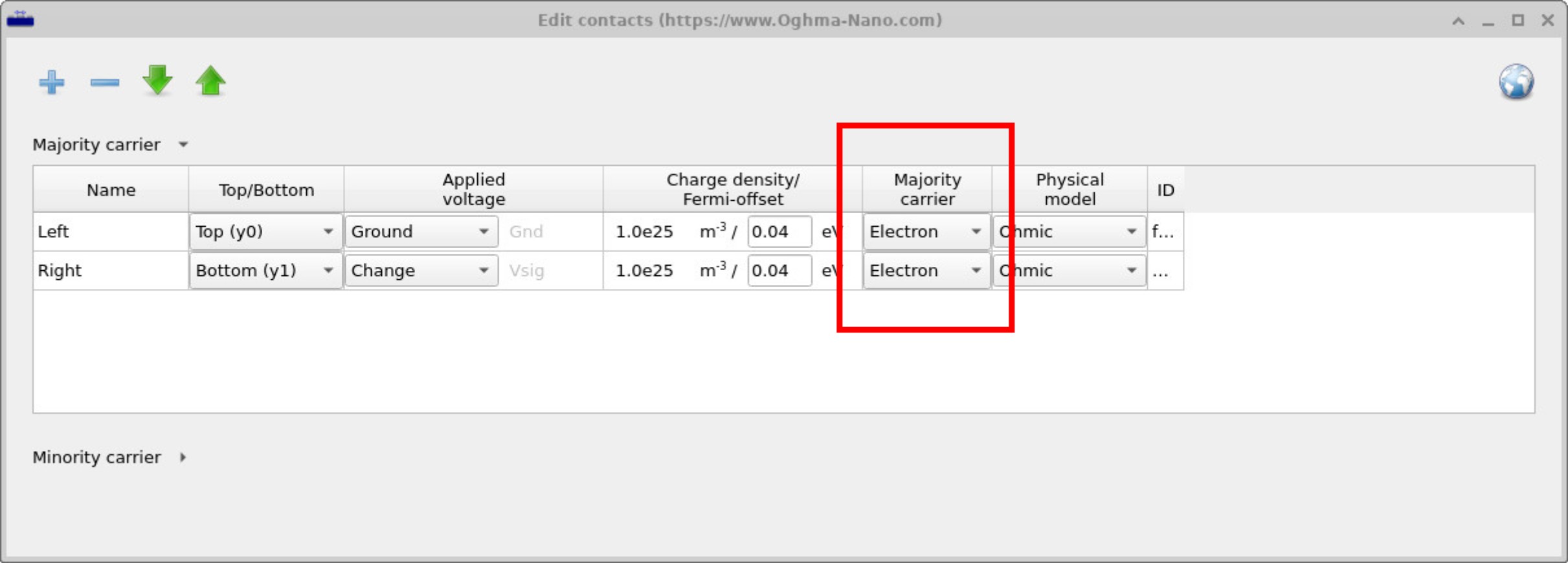
Before running the simulation by clicking Run Simulation (or pressing F9), we first need to examine the contacts. In the main window (??), the Contacts button is highlighted in the lower red box. Clicking this opens the contact editor. The contact editor allows both contacts to be set to the same carrier type. For example, they can both be defined as Hole contacts (??) or both as Electron contacts (??). In other words, you select one carrier type and apply it to both sides of the device.
This setup is very different from a solar cell, where the two contacts must be different—one electron contact and one hole contact. It does not matter which side is which, but the asymmetry is essential to separate charges and drive current. In SCLC measurements, however, the symmetry is deliberate. If both contacts are set to Electron, the device measures the electron mobility. If both are set to Hole, it measures the hole mobility. The logic is simple: the contacts inject the carrier type they are configured for, and that carrier dominates transport through the device.
Step 3: Check the simulation is running in the dark
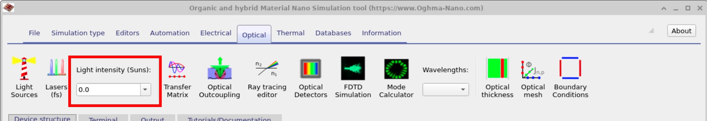
SCLC is almost always performed in the dark. Before running the experiment, make sure the simulation is also in dark conditions. This is done from the Optical ribbon by setting Light intensity (Suns) to 0.0, as shown in ??.
Step 4: Turn on parameter sweep output
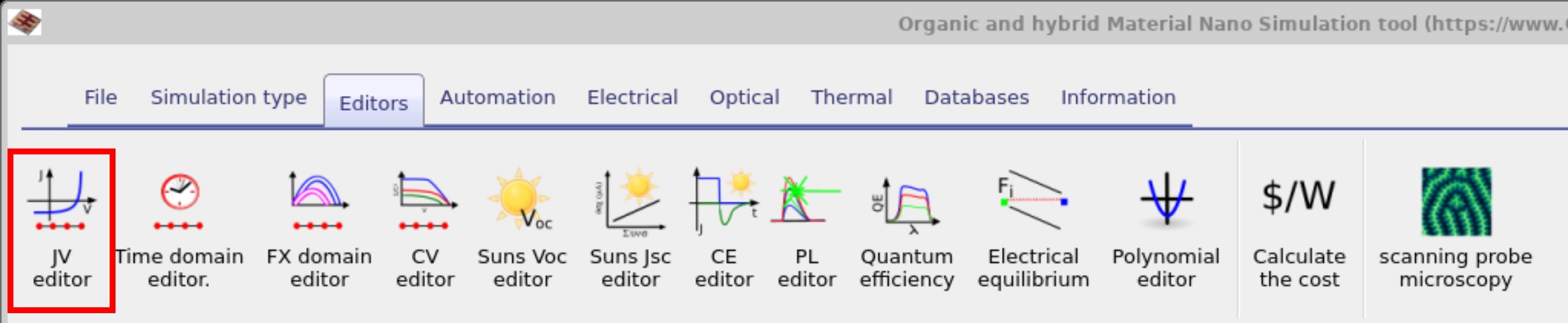
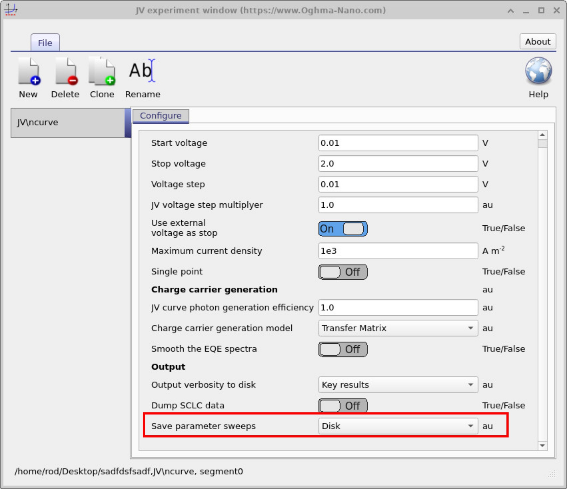
The final step before running the SCLC simulation is to open the JV editor, which you can access from the Editors → JV editor ribbon in the main window (??). This brings up the JV configuration window (??).
In this window, make sure that Save parameter sweeps is set to Disk, as shown at the bottom of ??. Enabling this option ensures that key device parameters—such as mobility, carrier densities, and other electrical quantities—are recorded as a function of applied voltage. Instead of producing simple 1D snapshots, the software integrates these values across the device and stores them so they can be plotted against voltage later. This is essential for SCLC analysis because it lets us see how the mobility evolves with voltage and determine the values extracted from the SCLC curves.
By default, this feature is often turned off because writing sweep data to disk can slow down simulations. In most cases you want to minimise disk output to keep runs efficient. However, for SCLC it is worth enabling despite the extra time required, since without it you would not be able to properly analyse mobility trends in the device.
Step 5: Run the SCLC simulation
Once the SCLC simulation is fully prepared—by setting both contacts to either Hole or Electron, ensuring the light is off, and enabling the Save Parameter Sweep option—you are ready to run. Return to the main window and start the simulation by clicking the Play button or pressing F9.
When the run completes, open the Output tab
(??).
Here you will see the standard simulation output, including jv.csv
and the sweep directory. Double-clicking on jv.csv opens the JV plot
(??),
which shows a typical SCLC curve. Pressing L followed by Shift+L
switches both axes to logarithmic scaling, making it easier to identify
the SCLC regime in the data.
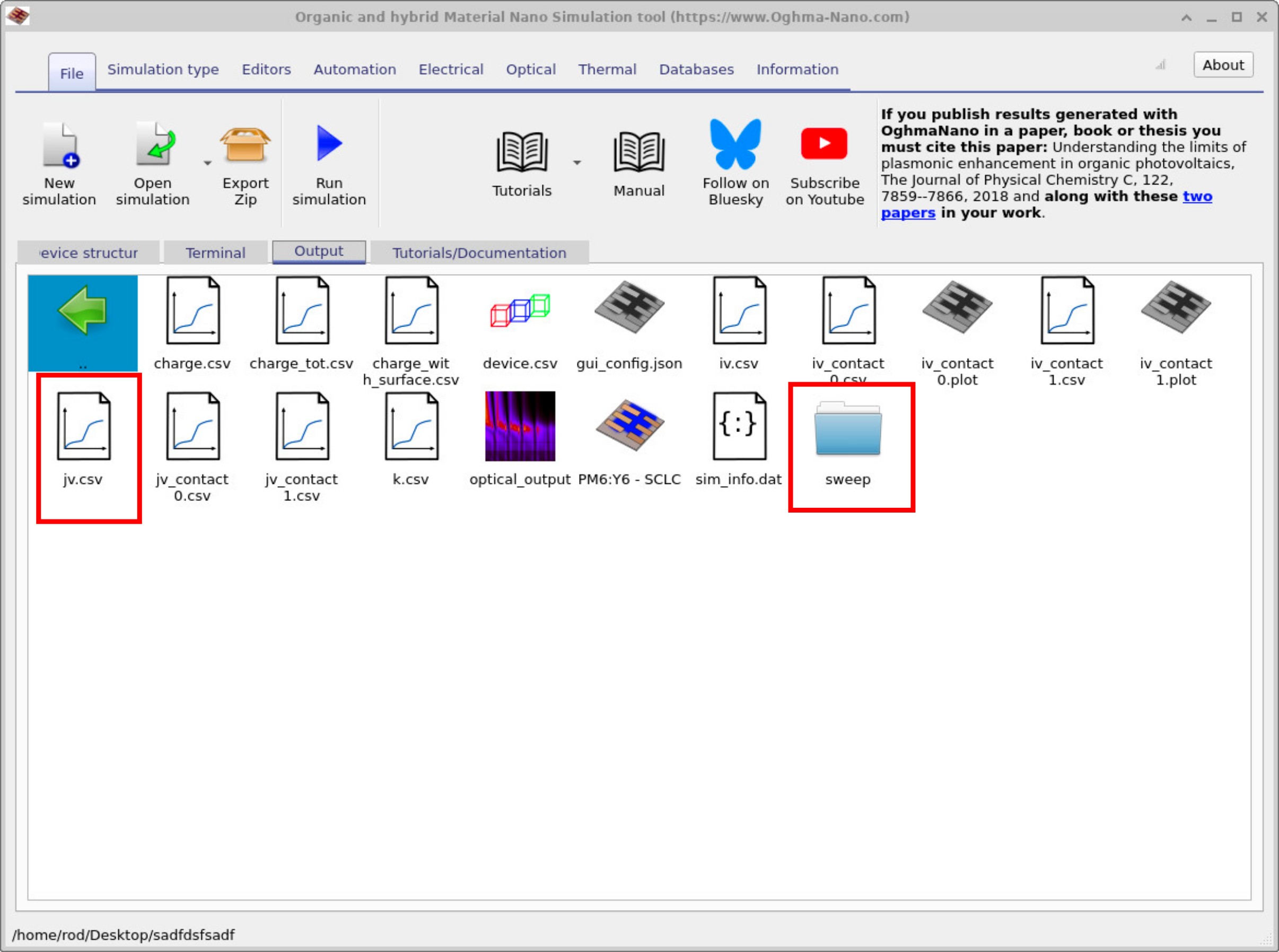
sweep directory.
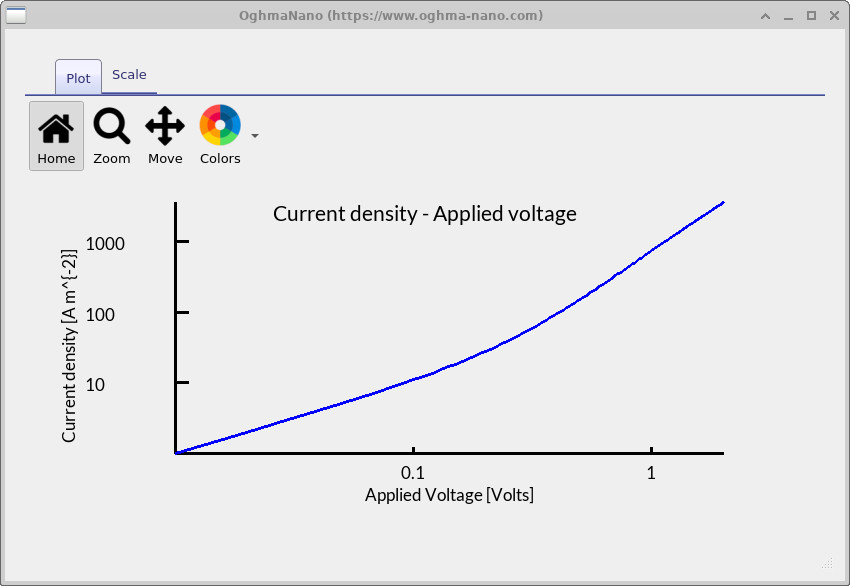
jv.csv and press L then Shift+L to plot on log–log axes. The JV curve reveals the SCLC regime.
Step 6: Extract mobility using the Mott–Gurney law
To determine the charge carrier mobility from an SCLC measurement, we use the Mott–Gurney law, which relates the measured current density to the applied voltage under trap-free conditions. The key step is to identify the SCLC regime in the JV curve, measured in the dark (??). The SCLC regime occurs once carrier injection from the contacts is efficient enough that the current is no longer limited by thermally generated carriers, but instead by the build-up of space charge in the device. In this regime the current density increases quadratically with voltage, following the relation \( J \propto V^2 \).
On a log–log plot of current density versus voltage, the SCLC regime can be recognised by a straight-line region with a slope of approximately 2.0. At lower voltages the slope is closer to 1.0, reflecting ohmic conduction dominated by equilibrium carriers. At higher voltages the current may deviate from quadratic behaviour again if trap filling, series resistance, or high-field effects become important. The mobility should therefore be extracted specifically from the intermediate voltage region where the slope is near 2, as this corresponds to the trap-free SCLC condition assumed in the Mott–Gurney law.
The Mott–Gurney expression assumes trap-free transport, ohmic injection, a single carrier type, uniform mobility, negligible diffusion current, and no significant series resistance. For a trap-free space-charge-limited current, the current density is given by
$$ J = \frac{9}{8}\,\varepsilon \mu \frac{V^2}{L^3}. $$
Rearranging for the mobility:
$$ \mu = \frac{8}{9} \cdot \frac{J L^3}{\varepsilon V^2}. $$
Substituting representative values:
- \( L = 100~\text{nm} = 1.0\times10^{-7}~\text{m} \;\;\Rightarrow\;\; L^3 = 1.0\times10^{-21}~\text{m}^3 \)
- \( \varepsilon_r = 3.0 \), \( \varepsilon_0 = 8.85\times10^{-12}~\text{F·m}^{-1} \), so \( \varepsilon = 2.655\times10^{-11}~\text{F·m}^{-1} \)
- \( V = 1.0~\text{V} \)
- \( J \approx 1.0\times10^{3}~\text{A·m}^{-2} \)
Now:
$$ \mu = \frac{8}{9} \cdot \frac{ (1.0\times10^{3})(1.0\times10^{-21}) } { (2.655\times10^{-11})(1.0^2) } = 3.35\times10^{-8}~\text{m}^2\text{V}^{-1}\text{s}^{-1}. $$
In cgs units, this corresponds to approximately \(3.35\times10^{-4}~\text{cm}^2\text{V}^{-1}\text{s}^{-1}\).
This worked example shows how the mobility can be extracted directly from the JV curve in the SCLC regime, using the Mott–Gurney relation.
Step 7: Plot simulated mobility inside the device
One of the real strengths of simulation is that you are not restricted to the
predictions of analytical models. Instead, you can look directly inside the
simulated device and examine how physical quantities evolve as the voltage is
applied. In this case, we can explore the results stored in the sweep folder,
shown in
??.
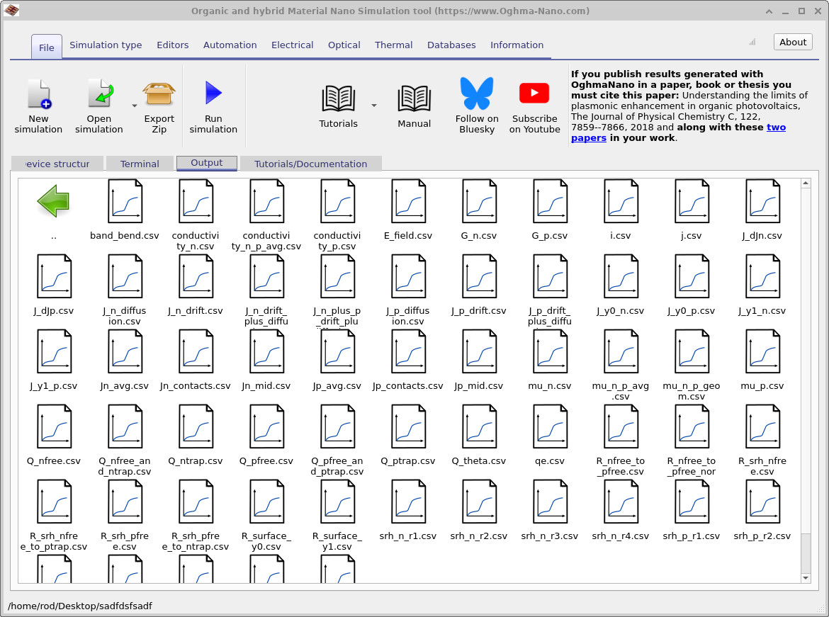
Opening this folder brings up a list of files
(??)
that contain device parameters saved as a function of voltage. These include
generation rates, carrier densities, recombination rates, and many other quantities.
For mobility analysis, the key files are mun.csv and mup.csv,
which report the simulated electron and hole mobilities. The file you choose depends
on whether you configured the device with electron or hole contacts earlier.
In this example, we are interested in electron transport, so we examine the
mun.csv output, shown in
??.
This plot reveals how the mobility changes with applied voltage.
The increasing trend arises in devices that contain traps. As the bias grows, more traps are filled and additional carriers are released into free states, leading to an apparent rise in mobility. This behaviour goes beyond the simple Mott–Gurney description and highlights the value of simulation: it not only reproduces the current–voltage curve, but also lets us see the underlying physical processes that shape device performance.
sweep directory, which can be accessed from the
Output tab. Here, many device parameters are stored and can be plotted as
a function of voltage.
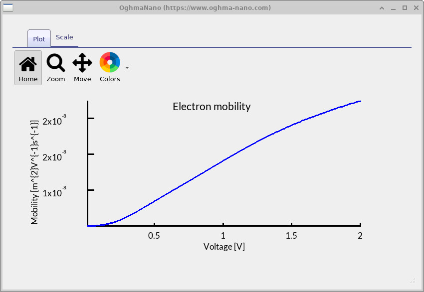
sweep directory, open the electron mobility result to view mobility as a function of voltage.
Comparing the analytical result from Section 5 with the numerical result from Section 6, we obtain an analytical mobility of approximately \(3.35\times10^{-8}\ \mathrm{m^2\,V^{-1}\,s^{-1}}\) versus a simulated value of about \(2\times10^{-8}\ \mathrm{m^2\,V^{-1}\,s^{-1}}\) for the SCLC case. The discrepancy is relatively small here, but it highlights a common outcome when contrasting analytical and numerical approaches: simplified analytical models (e.g., ideal, trap-free Mott–Gurney assumptions, perfectly ohmic injection, uniform fields, no series resistance or field-dependence) can differ from full device simulations that resolve traps, spatial variations, and non-ideal contacts. As a result, analytical and numerical values need not match exactly—even in SCLC—yet their trends should be consistent.
← Return to the introduction to organic electronics for a broader overview of the topic.