OghmaNano’s electrical model is a fully-coupled 1D/2D drift–diffusion solver designed for both crystalline and highly disordered semiconductors — including organics, perovskites, and amorphous silicon. While it shares the same core drift–diffusion framework as many other tools, it goes further by explicitly solving the Shockley–Read–Hall (SRH) trapping and recombination equations as a function of both energy and position.
This approach captures effects such as:
When simulating ordered materials, trap states can simply be disabled for a standard crystalline semiconductor model.
The solver uses a finite-difference discretisation of the coupled drift–diffusion, continuity, and Poisson equations, solved self-consistently via Newton–Raphson iteration. Adaptive time-stepping is available for transient simulations, ensuring stability across fast and slow processes. Optical generation profiles from the built-in optical solvers (uniform, exponential decay, or full transfer matrix) can be coupled directly into the electrical simulation.
In organics, the conduction and valence bands correspond to the LUMO and HOMO levels:
$$E_{LUMO} = -\chi - q\phi$$ $$E_{HOMO} = -\chi - E_g - q\phi$$The internal electrostatic potential distribution is obtained by solving Poisson’s equation:
$$\nabla \cdot \epsilon_0 \epsilon_r \nabla \phi = q (n_{f} + n_{t} - p_{f} - p_{t} - N_{ad} + - N_{ion} + a)$$where:
Free carriers can be treated using either:
Maxwell–Boltzmann statistics:
$$n_{l} = N_c \exp\left(\frac{F_n - E_{c}}{kT}\right)$$ $$p_{l} = N_v \exp\left(\frac{E_{v} - F_p}{kT}\right)$$Fermi–Dirac statistics:
$$n_{free}(E_{f},T) = \int^{\infty}_{E_{min}} \rho(E) f(E,E_{f},T) \, dE$$ $$p_{free}(E_{f},T) = \int^{\infty}_{E_{min}} \rho(E) f(E,E_{f},T) \, dE$$where:
$$f(E) = \frac{1}{1 + e^{(E-E_f)/kT}}$$For Fermi–Dirac statistics, free carriers are assumed to move in a parabolic band:
$$\rho(E)_{3D} = \frac{\sqrt{E}}{4\pi^2} \left( \frac{2m^{*}}{\hbar^2} \right)^{3/2}$$The average carrier energy is then:
$$\bar{W}(E_{f},T) = \frac{\int^{\infty}_{E_{min}} E \rho(E) f(E,E_{f},T) \, dE}{\int^{\infty}_{E_{min}} \rho(E) f(E,E_{f},T) \, dE}$$
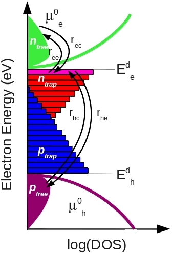 Figure 2: A 0D energy slice through the model. |
To describe charge becoming trapping into trap states and recombination associated with those states the model uses Shockley-Read-Hall (SRH) theory. A 0D depiction of this SRH recombination and trapping is shown in figure 2. The free electron and hole carrier distributions are labeled as \(n_{free}\) and \(p_{free}\) respectively. The trapped carrier populations are denoted with \(n_{trap}\) and \(p_{trap}\), they are depicted with filled red and blue boxes. SRH theory describes the rates at which electrons and holes become captured and escape from the carrier traps. If one considers a single electron trap, the change in population of this trap can be described by four carrier capture and escape rates as depicted in figure 2. The rate \(r_{ec}\) describes the rate at which electrons become captured into the electron trap, \(r_{ee}\) is the rate which electrons can escape from the trap back to the free electron population, \(r_{hc}\) is the rate at which free holes get trapped and \(r_{he}\) is the rate at which holes escape back to the free hole population. Recombination is described by holes becoming captured into electron space slice through our 1D traps. Analogous processes are also defined for the hole traps.
For each trap level the carrier balance
$$\frac{\delta n_t}{\partial t}=r_{ec}-r_{ee}-r_{hc}+r_{he}$$is solved, giving each trap level an independent quasi-Fermi level. Each point in position space can be allocated between 10 and 160 independent trap states. The rates of each process \(r_{ec}\), \(r_{ee}\), \(r_{hc}\), and \(r_{he}\) are give in table 1 below. The escape probabilities are given by:
$$e_n=v_{th}\sigma_{n} N_{c} exp \left ( \frac{E_t-E_c}{kT}\right )$$and
$$e_p=v_{th}\sigma_{p} N_{v} exp \left ( \frac{E_v-E_t}{kT}\right )$$where \(\sigma_{n,p}\) are the trap cross sections, \(v_{th}\) is the thermal emission velocity of the carriers, and \(N_{c,v}\) are the effective density of states for free electrons or holes. The distribution of trapped states (DoS) is defined between the mobility edges as
$$\rho^{e/h}(E)=N^{e/h}exp(E/E_{u}^{e/h})$$
Table 1: SRH capture escape rates |
where, \(N_{e/h}\) is the density of trap states at the LUMO or HOMO band edge in states/eV and where \(E_{U}^{e/h}\) is slope energy of the density of states. The value of \(N_{t}\) for any given trap level is calculated by averaging the DoS function over the energy (\(\Delta E\) ) which a trap occupies:
$$N_{t}(E)=\frac{\int^{E+\Delta E/2}_{E-\Delta E/2} \rho^{e}{E} dE}{\Delta E}$$The occupation function is given by the equation,
$$f(E_{t},F_{t})=\frac{1}{e^{\frac{E_{t}-F_{t}}{kT}}+1}$$Where, \(E_{t}\) is the trap level, and \(F_{t}\) is the Fermi-Level of the trap. The carrier escape rates for electrons and holes are given in table 1.
Free-to-free recombination is described using equation
$$R_{free}=k_{r}(n_{f}p_{f}-n_{0}p_{0})$$Auger recombination is included in the model as
$$R^{AU}=(C^{AU}_{n}n+C^{AU}_{p}p)(np-n_{0}p_{0})$$where \(C^{AU}_{n}\) and \(C^{AU}_{p}\) are the Auger coefficient of electrons and holes in \(m^6 s^{-1}\). This can be set in the electrical paramter editor.
To describe charge carrier transport, the bi-polar drift-diffusion equations are solved in position space for electrons,
$$\boldsymbol{J_n} = q \mu_e n_{f} {\nabla E_{c}} + q D_n {\nabla n_{f}}$$and holes,
$$\boldsymbol{J_p} = q \mu_h p_{f} {\nabla E_{v}} - q D_p {\nabla p_{f}}$$Conservation of charge carriers is forced by solving the charge carrier continuity equations for both electrons,
$$\nabla \boldsymbol{J_n} = q (R-G+\frac{\partial n}{\partial t})$$and holes
$$\nabla \boldsymbol{J_p} = - q (R-G+\frac{\partial p}{\partial t})$$where \(R\) and \(G\) are the net recombination and generation rates per unit volume respectively.
Three optical generation profiles are available:
OghmaNano’s drift–diffusion engine now supports 1D, 2D, and full 3D device geometries with the same coupled physics (Poisson + electron/hole continuity, SRH trapping/recombination, optional ionic/excitonic terms). This lets you prototype quickly in 1D, validate lateral effects in 2D, and then study realistic architectures in 3D without changing tools.
For power users, the solver exposes a Lua microcode layer that controls the Newton iteration schedule and active physics at each micro-step. This enables ADI-style axis sweeps, block solves, and custom update schedules without recompiling the core.
solve_pos_*), e/h currents (solve_je_*/solve_jh_*), SRH traps, ions, singlets.step_x, step_y, step_z (−1, 0, +1).a = dd_solver()
local count, cont = 0, true
while cont do
-- Pass 1: Z-dominant
a.set_newton_state("x")
a.step_x, a.step_y, a.step_z = 1, -1, -1
a.solve_pos_x, a.solve_pos_y, a.solve_pos_z = false, true, true
a.solve_je_x, a.solve_je_y, a.solve_je_z = 0, true, true
a.solve_jh_x, a.solve_jh_y, a.solve_jh_z = 0, true, true
a.solve_srh_e, a.solve_srh_h = true, true
a.solve_nion, a.solve_singlet = false, false
local e1 = a:run()
-- Pass 2: X-dominant
a.set_newton_state("z")
a.step_x, a.step_y, a.step_z = -1, -1, 1
a.solve_pos_x, a.solve_pos_y, a.solve_pos_z = true, true, false
a.solve_je_x, a.solve_je_y, a.solve_je_z = true, true, false
a.solve_jh_x, a.solve_jh_y, a.solve_jh_z = true, true, false
local e2 = a:run()
local tot = e1 + e2
print(("iter=%d residual=%.3e"):format(count, tot))
cont = not (tot < 1e-7 or count > 10)
count = count + 1
end
set_newton_state("x"|"y"|"z"|"all") — select block/state for the next micro-step.step_x, step_y, step_z — sweep direction per axis: +1 forward, -1 reverse, 0 freeze.solve_pos_* — include Poisson coupling along that axis in the Jacobian.solve_je_*, solve_jh_* — include electron/hole current equations per axis.solve_srh_e, solve_srh_h — update trap populations (electrons/holes).solve_nion, solve_singlet — optional ionic/excitonic updates this pass.:run() — executes one micro-iteration and returns a scalar residual.This advanced control is ideal for tackling tough bias points, heavy trapping, or mobile-ion dynamics in full 3D meshes, and for prototyping new iteration strategies without recompilation.
Want to dive deeper?
👉 Check out the core physical modules in the manual and start simulating right away.