Advanced OFET and 2D Device Simulation Software
1. Introduction
OghmaNano provides an advanced OFET simulation framework for modelling organic field-effect transistors and related 2D thin-film devices using a self-consistent multi-physics approach. The simulator combines drift–diffusion transport, Poisson electrostatics, contact boundary conditions, and trap-state modelling to resolve how charge moves through planar transistor structures.
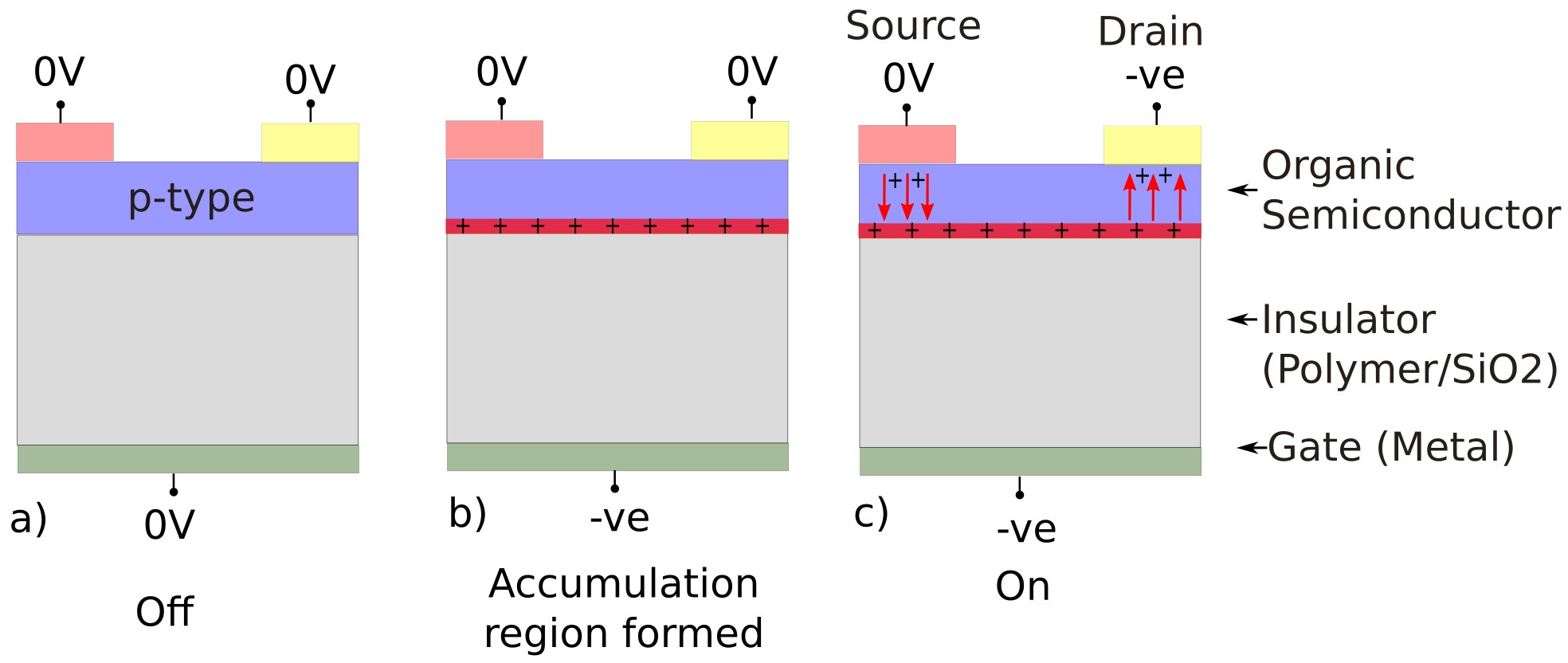
Unlike 1D device models, OFET simulation requires the lateral and vertical geometry of the device to be treated explicitly. Gate, source, and drain fields interact across strongly anisotropic structures, and current is controlled by a thin accumulation channel at the semiconductor–insulator interface. OghmaNano therefore solves OFETs directly in 2D, allowing the user to study accumulation, depletion, injection, contact effects, and channel formation in realistic layouts. The basic operating principle is illustrated in Figure ??, while the default simulation geometry is shown in Figure ??.
This makes the software useful both for interpreting transistor measurements and for virtual device design before fabrication. A guided walk-through is available in Figure ??, and the full tutorial sequence begins with Part A: simulate your first OFET.
✨ What you can do with OghmaNano
- Simulate realistic OFET geometries: define top-gate or bottom-gate structures with explicit source, drain, and gate geometry.
- Model gate-controlled channel formation: resolve surface charge accumulation, depletion, and lateral current flow in 2D.
- Include trap-limited physics: account for trap states and energetic disorder in the semiconductor bulk or at the semiconductor–dielectric interface.
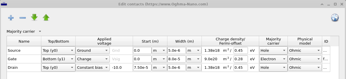
- Study contact engineering: investigate source/drain injection, gate biasing schemes, and contact placement using the contact editor shown in Figure ??.
- Visualise internal operation: plot 2D and 3D maps of potential, charge density, trap occupancy, and current flow.
- Work with challenging device dimensions: simulate large aspect-ratio transistor structures that are poorly captured by 1D approximations.
- Extract physically meaningful parameters: interpret transfer and output curves in terms of mobility, trap density, threshold behaviour, and contact effects.
Try an OFET example.
👉 Start with the Quick Start OFET tutorial, then move on to visualising OFET results in 2D and 3D, editing electrical parameters, and solver stability and meshing.
2. Why OFET simulation needs a 2D model
In an OFET, the gate does not drive current directly through the device. Instead, it creates an electric field across the dielectric, which induces a thin conducting channel at the semiconductor–insulator interface. Once this channel is formed, the source–drain bias drives current laterally along it. This behaviour is inherently two-dimensional: the vertical field from the gate controls the lateral current flow between source and drain.
For this reason, physically realistic OFET simulation requires more than a simple 1D approximation. OghmaNano resolves the internal electrostatic potential, carrier density, and current distribution directly in 2D, making it possible to understand how geometry, bias, and material parameters shape transistor behaviour.
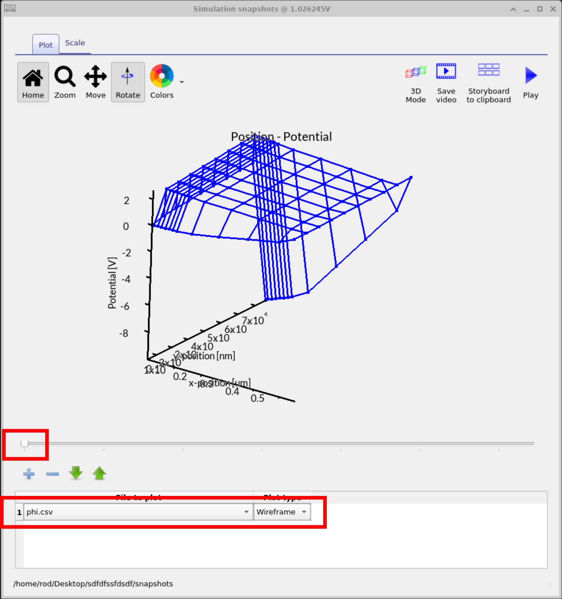
The resulting internal state can be visualised directly. For example, the electrostatic potential map shown in Figure ?? shows how the gate and drain biases redistribute the internal field across the device. This kind of output is particularly useful when diagnosing channel formation, fringe fields, or failure to turn on properly.
3. Device structure, contacts, and active layers
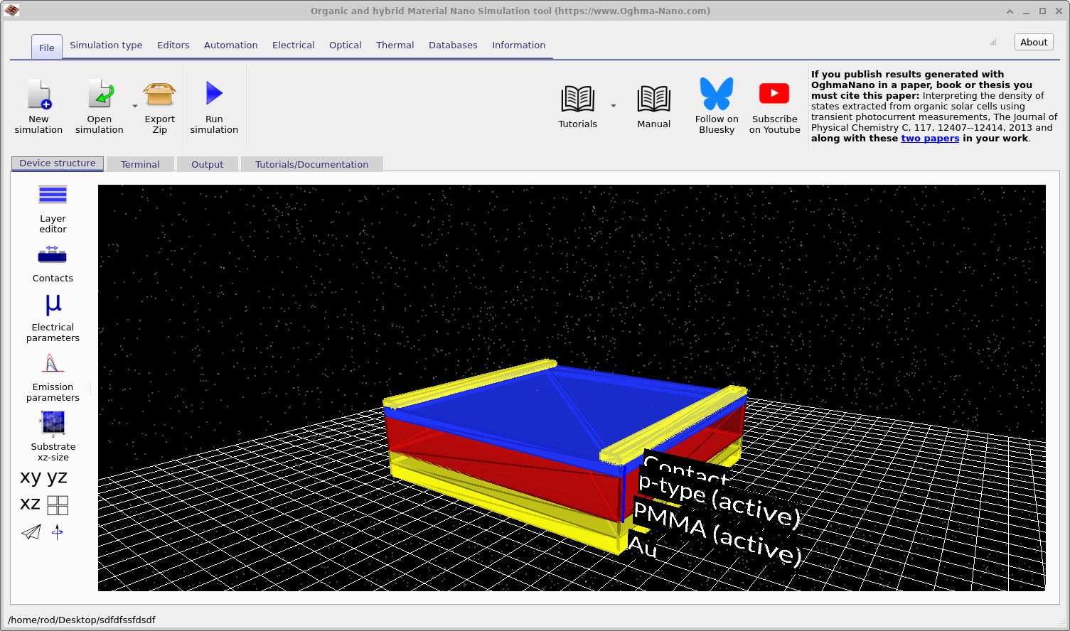
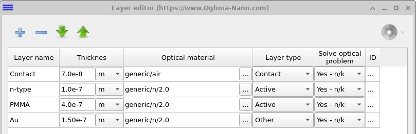
The transistor stack itself is defined in the layer editor shown in Figure ??. In OghmaNano, layers can be marked as electrically active or inactive, making it possible to separate conducting semiconductor regions from passive dielectric layers and structural elements.
The contact geometry is then defined in the contact editor shown in Figure ??. This is important for 2D transistor simulation because contact position and width affect how the solver applies source, gate, and drain boundary conditions across the mesh.
This makes it possible to study not only standard OFET layouts, but also more specialised structures where geometry, dielectric thickness, or contact placement strongly influence the measured response.
4. Visualising internal transistor operation
One of the strengths of OghmaNano is that it does not stop at the external transfer curve. During each simulation, the software writes internal solver variables to the snapshots directory, allowing the user to inspect electrostatic potential, charge density, trap density, and related quantities as a function of bias.
These outputs can be viewed in both 2D and 3D using the snapshots viewer, making it possible to track how the internal state evolves during the voltage sweep. This is especially valuable for OFETs, where the spatial location of the conducting channel and the effect of the gate field are central to device operation.
Useful next steps include visualising OFET results in 2D and 3D, editing semiconductor and insulator parameters, and understanding solver stability and meshing in 2D transistor simulations.