OFET Simulation (Organic Field-Effect Transistor): Quick Start and JV Analysis
This OFET simulation tutorial introduces the basic theory of organic field-effect transistors before guiding you through a 2D p-type OFET simulation in OghmaNano.
1. Basic theory of a p-type Organic Field-Effect Transistor (OFET)
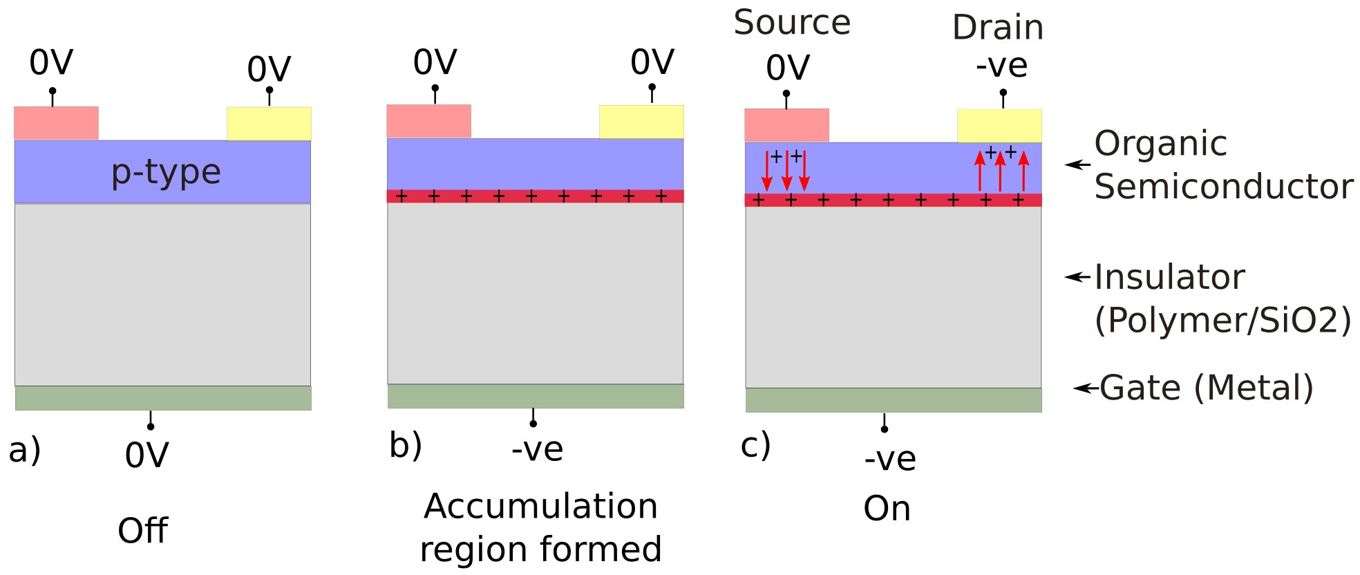
?? shows the structure of a typical OFET. A thin organic semiconductor layer (blue) is deposited on top of an insulating polymer/SiO2 layer (grey). Two contacts, the Source and Drain, are positioned on the top of the semiconductor to inject and collect charge carriers, while a third contact, the Gate (green), is located beneath the insulator to control the device operation.
In operation, the Gate electrode modulates the flow of charge carriers between the Source and Drain through the organic semiconductor layer. Applying a voltage to the Gate generates an electric field across the insulator, this causes a thin layer of charge to build up at the semiconductor-insulator interface (red), this is very much like the layer of charge that develops when a potential is applied to a capacitor. Depending on the material system, the dominant carriers can be holes (p-type) or electrons (n-type), in a p-type material a -ve potential is applied to form a layer of holes (this can be seen in ??b:). When a bias is applied between Source and Drain, these carriers drift through the induced channel and the device is turned on (??c). If the voltage applied to the gate is turned off, the charge channel disappears and the flow of charge carriers between Source and Drain stops. Generally, current level is governed by the Gate voltage: below a certain threshold, the channel remains insulating, while above it, channel conductivity increases with Gate bias. This field-effect control enables the OFET to operate as a switch or, in the linear regime, as an amplifier, with performance determined by factors such as carrier mobility, threshold voltage, and contact resistance.
The operation of the OFET is illustrated in ??a–c:
- Initial state — off (??a). With all terminals at 0 V, no charge is induced at the semiconductor–insulator interface. There is no conducting path between the Source and Drain, so the device remains off.
-
Gate bias - channel formation (??b).
Applying a negative voltage to the Gate creates an electric field across the insulator.
The field electrostatically attracts holes to the semiconductor–insulator interface,
forming a thin accumulation layer (the channel). With
VDS=0the device still carries no current, but the conductive channel is established. -
Drain bias - current flow (??c).
Applying a negative Drain voltage relative to the Source
(
VDS<0, Source ≈ 0 V) injects holes from the Source into the channel. Holes drift along the Gate-induced channel toward the Drain, producing the Drain current. A more negative Gate bias strengthens the accumulation channel and increases the current.
In essence, the gate’s electric field induces a conductive channel at the semiconductor–insulator interface. Current flows between source and drain only when this channel is present, allowing the OFET to operate as a voltage-controlled switch or as an amplifier. Removing the gate bias depletes the channel and turns the device off.
The description above illustrates a p-type OFET, where holes are the majority carriers. OFETs can also operate as n-type devices, in which electrons form the conduction channel (and a +ve voltage is applied to the gate), or as ambipolar devices, capable of transporting both holes and electrons depending on the applied bias. Although all three modes are possible, p-type OFETs remain the most common, because hole transport in organic semiconductors is typically more stable in ambient conditions and easier to achieve experimentally.
2. Quick start: running an OFET simulation
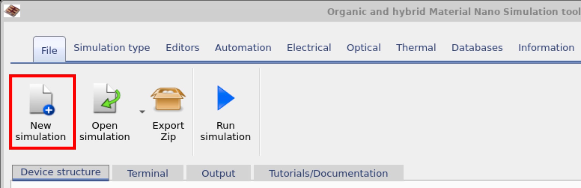
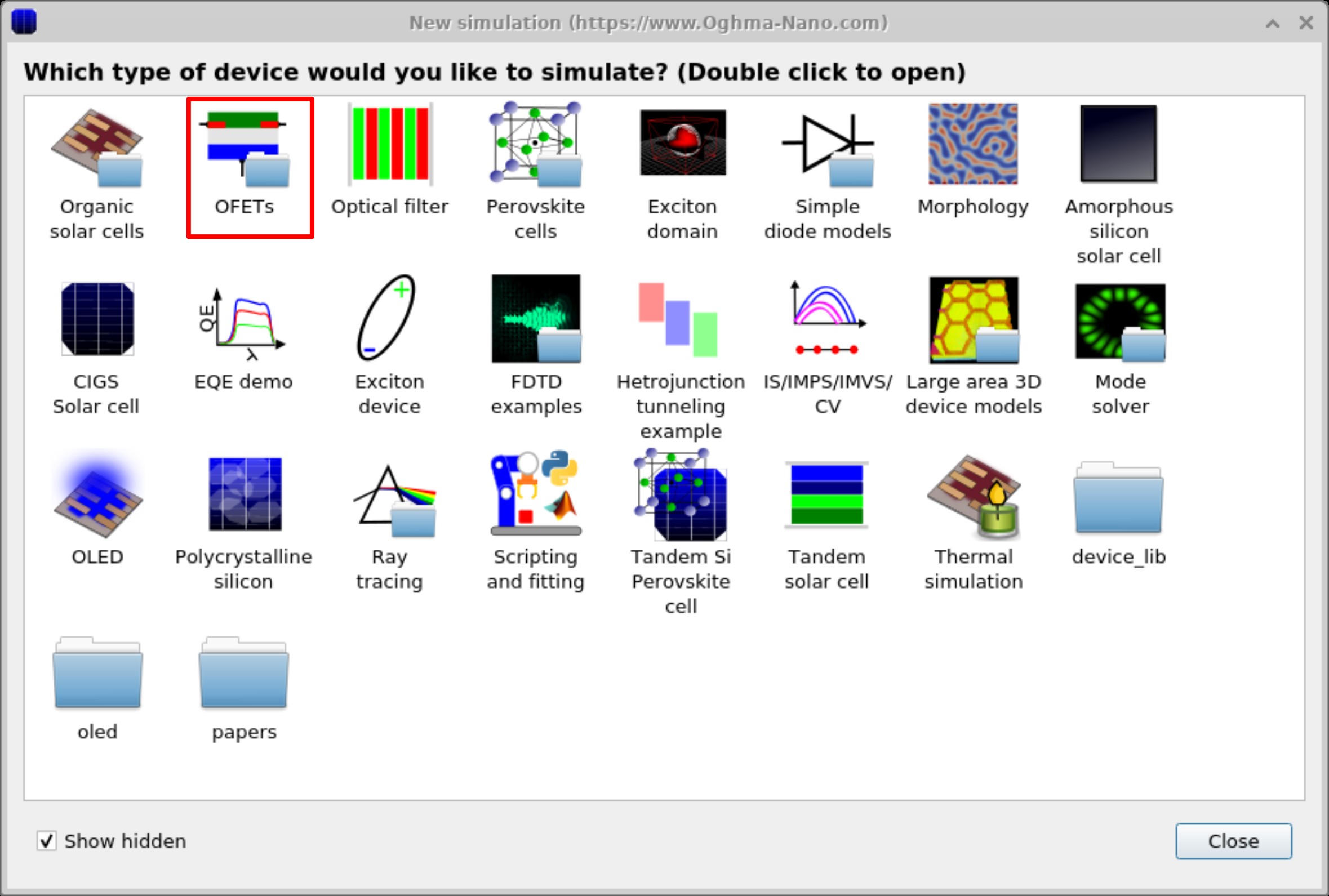
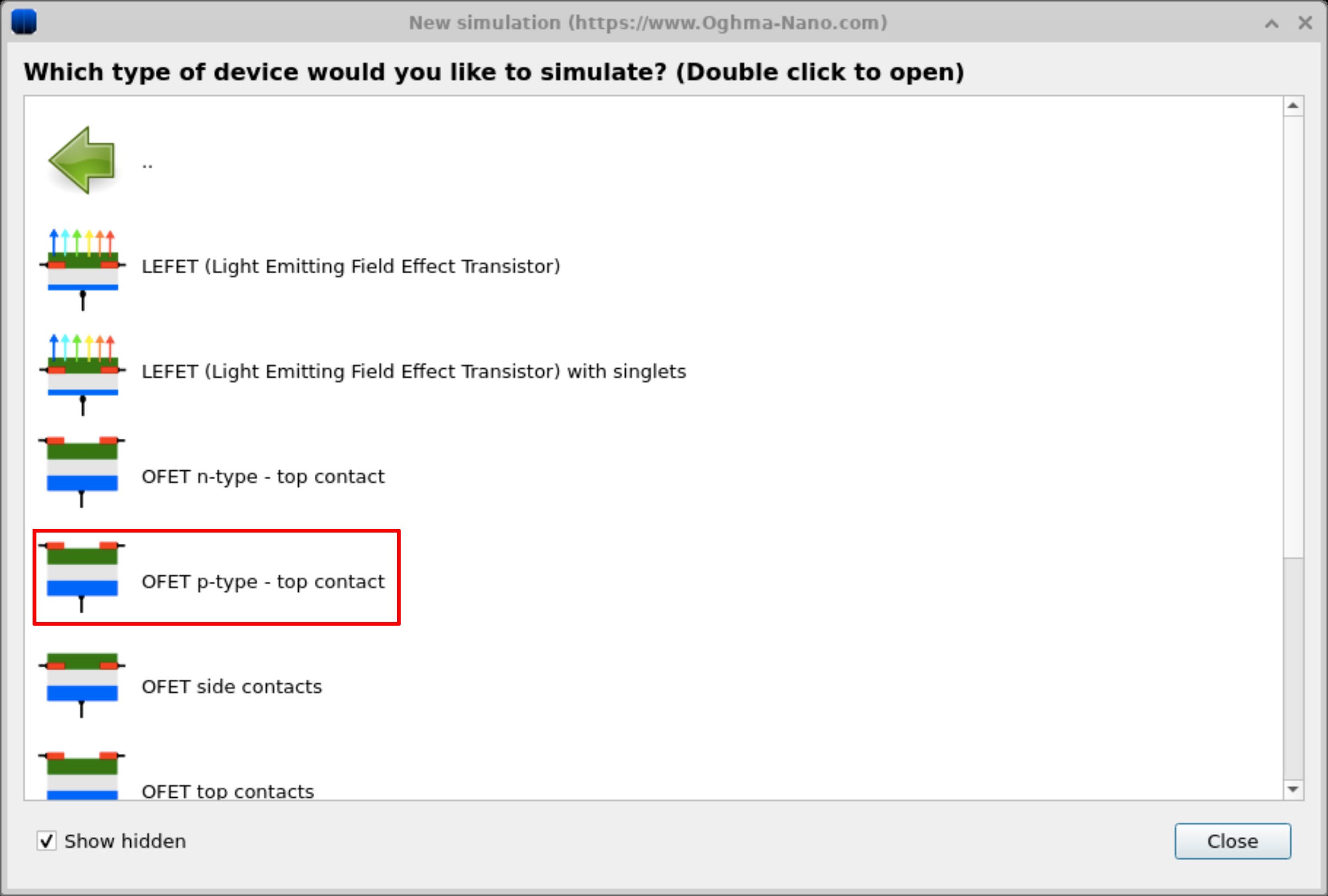
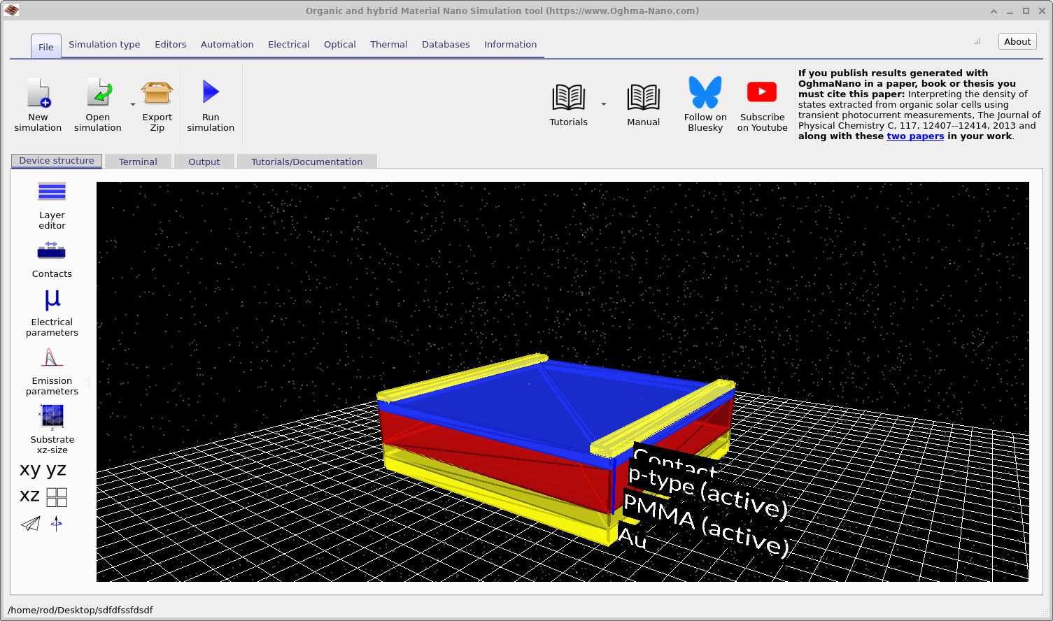
In this tutorial, we will focus on p-type MOSFETs with top contacts. P-type semiconductors are the most widely used in organic electronic devices because they typically exhibit higher hole mobility. To make a new OFET simulation, click on the New simulation button in the OghmaNano main window (??). Then in the new simulation window and double click on the OFET simulations (see figure ??). This will bring up the OFET sub menu, where other types of OFETs are also stored. For this example we will be looking using the "OFET p-type top contact" (??), double click on this and save the new simulation to disk.
Once you have saved the new simulation window, you should get a window looking like ??. Click and hold the left mouse button on the black background, then drag to rotate the simulation window and view the device in 3D. You can see that the device has three contacts, a gate, source and a drain. The source and drain are shown on the top of the simulation as gold bars, a semiconductor layer is shown in blue and an insulating later shown in red. The gate contact is visible at the bottom of the structure.
3. Running your first OFET simulation
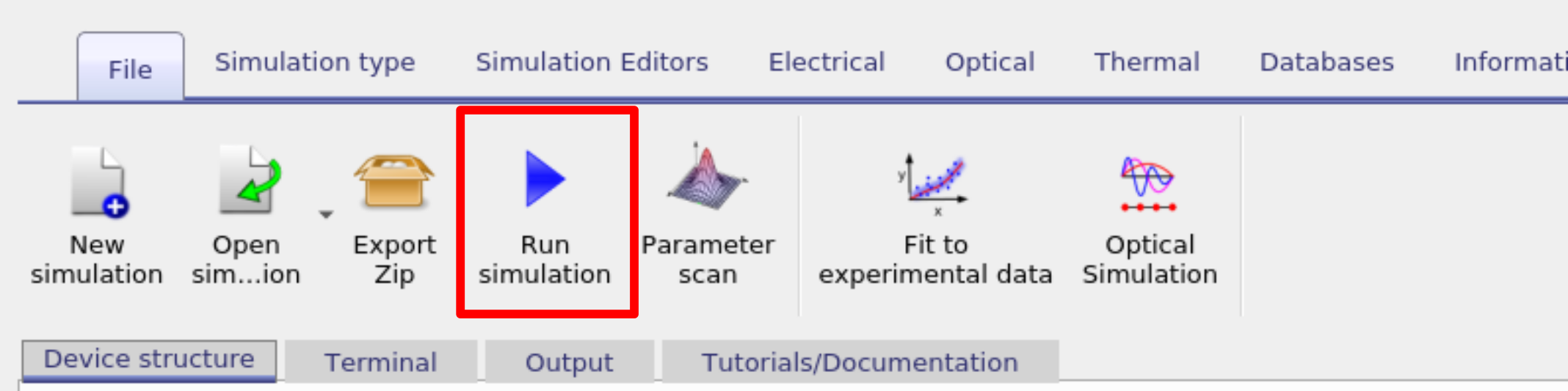
To start the simulation, click the Play button. Compared with 1D simulations, 2D simulations typically take longer because the solver must handle a mesh an increased number of mesh points. If traps are enabled, carrier capture/escape equations are also solved at every mesh point, further increasing the computational load. Generally speaking increasing the dimensionality of a problem quickly increases runtime and memory requirements.
jv_contact_0.csv, jv_contact_1.csv, jv_contact_2.csv), alongside
summary and diagnostic files such as charge.csv, device.csv, and sim_info.dat.
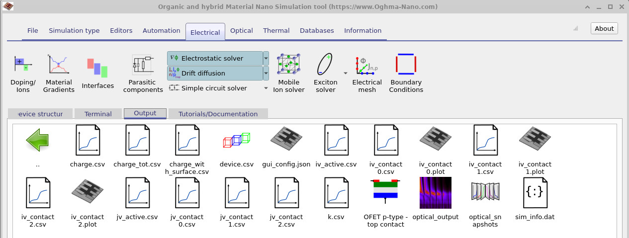
When the simulation finishes, open the Output tab. You’ll see more files than in a 1D case because an OFET has multiple contacts. This is because a JV curve is produced for each contact, each curve represents the current the flows or leaves the device through that contact. A summary of the files produced is given below.
| File name | Description |
|---|---|
| contact_iv0.dat | Current vs voltage curve for contact 0 |
| contact_iv1.dat | Current vs voltage curve for contact 1 |
| contact_iv2.dat | Current vs voltage curve for contact 2 |
| contact_jv0.dat | Current density vs voltage curve for contact 0 |
| contact_jv1.dat | Current density vs voltage curve for contact 1 |
| contact_jv2.dat | Current density vs voltage curve for contact 2 |
| snapshots/ | Simulation snapshots |
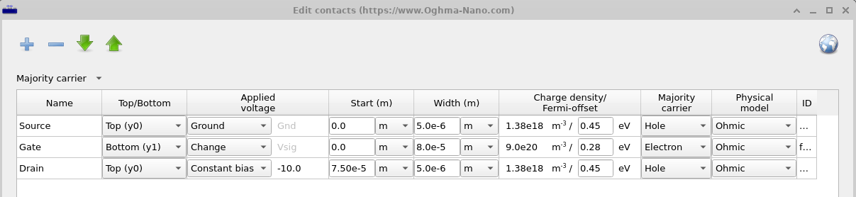
Double-click on the files jv_contact_0.csv, jv_contact_1.csv, and jv_contact_2.csv to inspect each contact’s curve. Contacts in OghmaNano are labelled from 0 to N in the order they are defined in the contact editor (see Figure
??), so in
this case Contact 0 will be the source, contact 1 will be the gate and contact 2 will be the drain. The contact editor has been described in detail in section 3.1.8, however because this is a 2D simulation another two extra columns have appeared. They are start and width. These define the start position of the contact on the x-axis and width which describes the width of the contact on the x-axis. The source starts at \(0~m\) and extends to \(5 \mu m\), the drain starts at \(75~\mu m\) and extends to \(5 \mu m\), while the gate starts at \(0~m\) and extends to cover the entire width of the device which is \(80~ \mu m\). Notice also that under the column Applied Voltage, the source is marked Ground this
means that 0V will be applied to the ground, the gate is marked change meaning that our voltage ramp as defined in the JV editor will be applied to this contact, and the drain is marked constant bias with a voltage of 10V, this means that a constant voltage of 10V will be applied to this contact. And thus we are scanning the gate contact while applying a constant voltage between the source and the drain.
??, ?? and ?? show the JV curves at each of the three OFET contacts. By looking at ?? and ?? you can see that as the gate voltage becomes more negative so does the current at the source and drain. We are applying a negative voltage to attract holes to the channel so that it can conduct. You can also see that there is no current at the Gate, this is because current is being blocked by the dielectric.
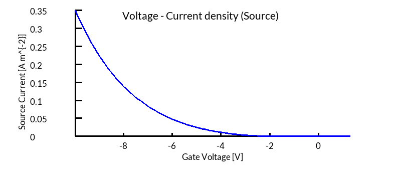
jv_contact0.csv - the source) of the OFET.
The negative sign indicates current leaving the device through this terminal.
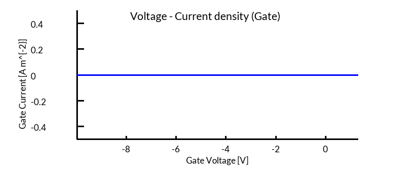
jv_contact1.csv - the gate).
Current remains close to zero because the gate is insulating.
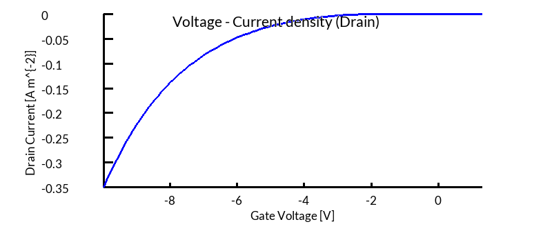
jv_contact2.csv - the drain).
The positive current corresponds to charge injection into the device.
👉 Next steps:
- Continue to Part B to learn about visualising OFET results in 2D and 3D, exploring current flow, charge densities, and device fields in more detail.
- Return to the introduction to organic electronics for a broader overview of the topic.