OFET Solver Stability: Mesh, Convergence and Simulation Errors
This section explains how to diagnose solver stability and convergence problems in 2D OFET simulations. One-dimensional simulations are usually stable and fast, but as the dimensionality increases from 1D to 2D and 3D, the number of coupled equations and linking terms grows rapidly. Poor mesh choices, unrealistic mobility values, badly resolved contacts or overly large bias steps can therefore cause the drift–diffusion solver to fail to converge.
Here we will deliberately push a few simple setups to provoke non-convergence, then diagnose why it happens and how to fix it. By reproducing these common failure modes yourself, you’ll learn to recognise the symptoms and apply the right remedies (e.g., adjusting the mesh, reducing bias step size, or moderating extreme material parameters) to recover a stable solution.
1. Solver instability from unrealistically low mobility
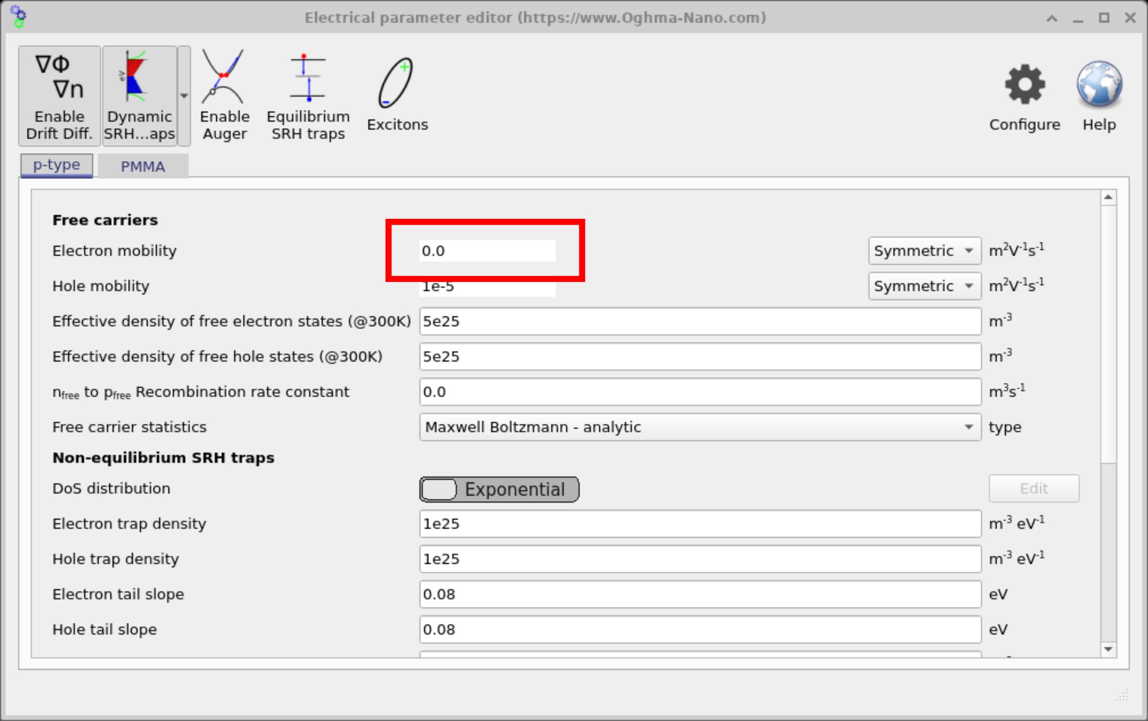
In many cases, convergence problems arise from non-physical input values. To illustrate this, we deliberately set the carrier mobility to 0 and examine the resulting errors. Of course, mobility is never truly zero in a real material—it always has a finite value—but this example shows what happens when the solver is given an unrealistic parameter. Mobility is configured in the
OFET electrical parameters editor. If the value is set outside a physically meaningful range, the drift–diffusion equations can become ill-conditioned or fail to converge.
Open the Electrical Parameters editor (Main window → Device tab) and set the mobility to 0, as shown in ??. Now run the simulation. You should see an error screen similar to ??, with two red boxes: a vertical box around the residual summary and a horizontal box near the crash message.
If you look at the vertical red box you can see f()=2.54e2 followed by other lines where f() is very large (e.g.
1e15, 1e5, 1e8, 1e7). Here, f() is the solver
residual error: a measure of how well the coupled equations are currently satisfied. Ideally, the solver residual would be exactly zero, although in practice this can never be achieved. A residual in the range of 1e−10 to 1e−8 indicates very good convergence, while values around 1e−1 are still acceptable.
By contrast, residuals in the hundreds (e.g. 2.54e2) - especially when accompanied by component values as large as 1e15-are a clear sign that the solver is struggling and the system has become unstable.
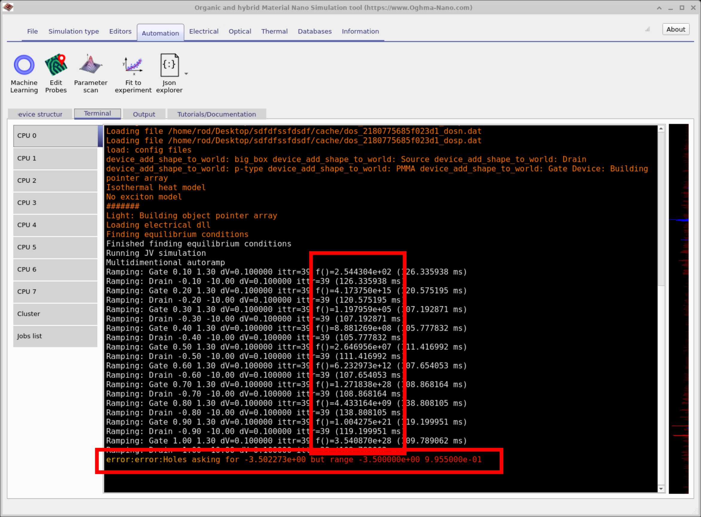
The horizontal red box typically reports why the run finally aborts: Holes asking for 3e5 but only defined in range [min, max]. This means the computed quasi-Fermi level has gone outside the tabulated range. Before starting, the model pre-tabulates relationships such as quasi-Fermi level vs. carrier density over a large energy range domain - indeed far larger than one would typically expect to find in a device. When the solver becomes unstable, the model can request unrealistic values far beyond that range; at that point the solver cannot evaluate the needed quantities and stops.
In short, by setting mobility to an unphysical value (μ = 0) we forced the equations into a regime that makes no physical sense, so the numerical method fails: large residuals, followed by a request for values outside the precomputed tables, and then a crash. It is important to note that this outcome is not a weakness of the model or a software bug.
By entering non-physical parameters, the solver is pushed into a regime where no mathematically or physically valid solution exists, and therefore it cannot provide a meaningful result.
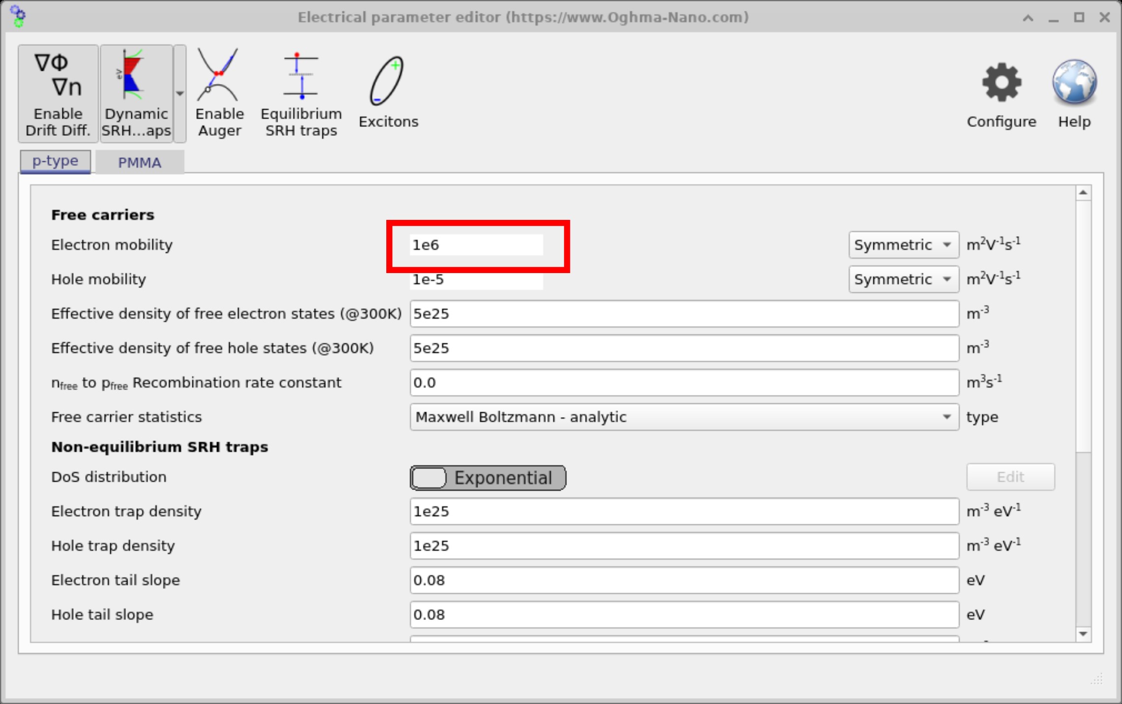
2. Solver instability from unrealistically high mobility
In this example we set the carrier mobility to μ = 1×10⁶ m²·V⁻¹·s⁻¹. This is an
intentionally unphysical value for a semiconductor drift–diffusion model: such a magnitude might be
associated with metallic conduction regimes rather than hopping/ band transport in organic or typical
semiconductors. In practice, you would not use a value this large for OFET simulations.
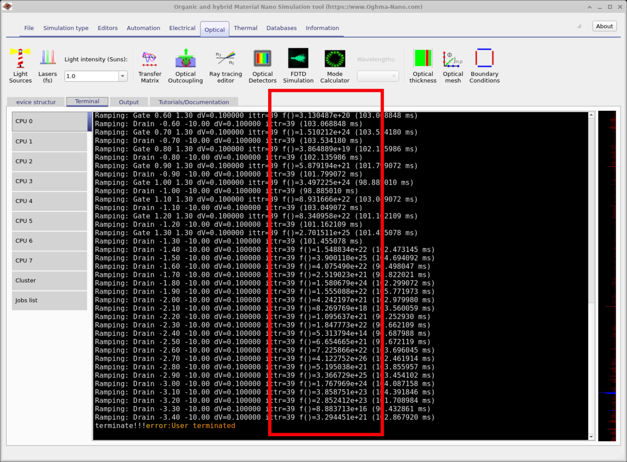
If you run the simulation with this setting, you can observe the solver struggling to converge. In the residual
readout (the box that reports f()) you will see extremely large errors—e.g.
1e24, 1e19, 1e21—that do not decay. It is normal for residuals to be
elevated during the first few iterations as the solver finds a consistent state, but they should quickly settle
toward small values. Persistently huge residuals are a clear indication that the system has become numerically
stiff or non-physical due to the chosen parameters.
The takeaway: avoid unrealistically high mobilities. Excessive transport coefficients make the PDE system very stiff, causing poor conditioning and non-convergence. Use physically reasonable μ values for your material system and re-run with moderate bias steps to restore stable behaviour.
3. Bad device structures and unresolved contacts
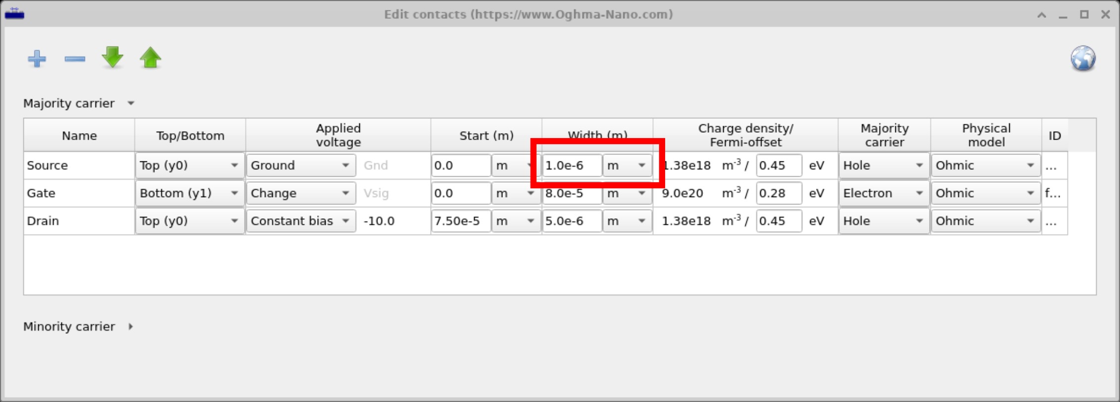
In this example we open the contact editor and set the contact width of the Source to a very small value (see ??) , to one micron. At first glance this may not seem problematic, but it creates a subtle issue: the simulation is based on a finite-difference mesh, where quantities such as electric field and carrier density are calculated only at the defined mesh points.
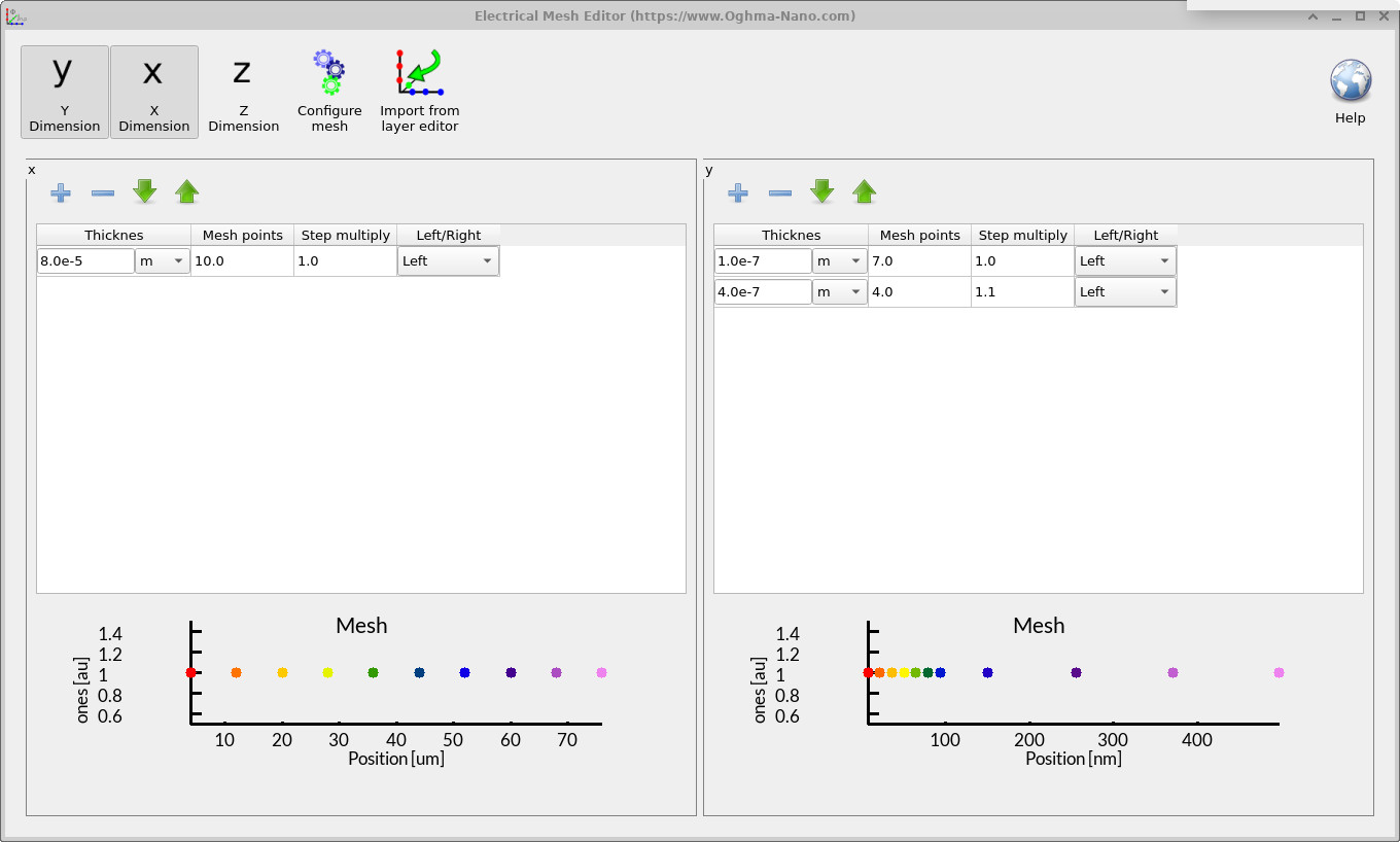
If you inspect the Electrical Mesh Editor (found under the Electrical tab), you will notice that this ultra-thin one-micron contact falls between mesh points (see ??). As a result, the contact is effectively “missed” by the finite-difference grid and never properly applied to the device structure. This creates a mismatch between the defined geometry and the numerical mesh, preventing the simulation from converging.
To fix this, you can either increase the thickness of the contact so that it overlaps at least one mesh point, or increase the mesh density (i.e. add more points) in the finite-difference grid so the contact is captured correctly.
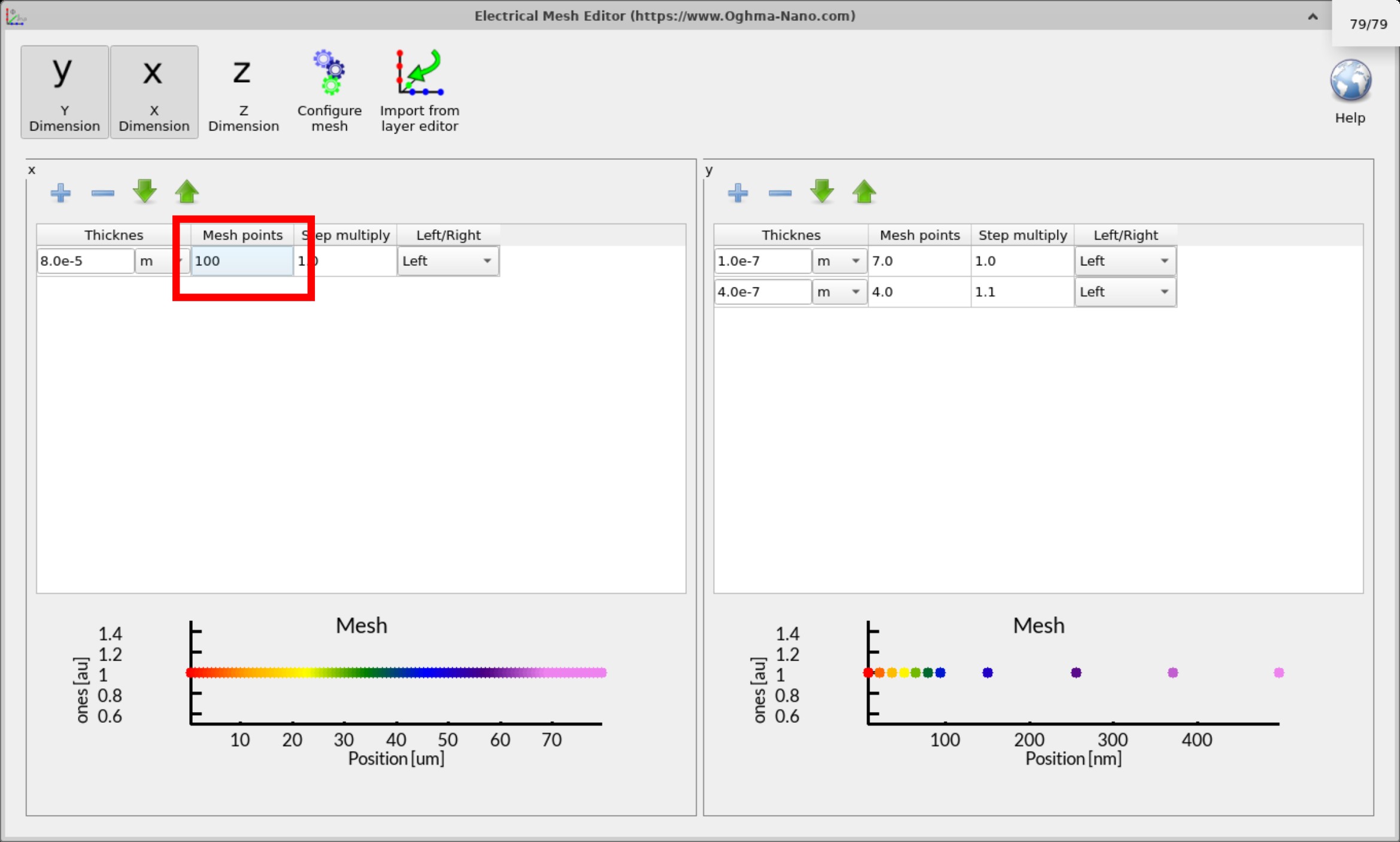
4. Mesh density, convergence and over-refinement
A common preconception when starting with finite-difference models is that more mesh points automatically produce more accurate results. The reasoning often goes: “five mesh points must be poor, but one thousand must be excellent.” In practice, this is not the case.
OghmaNano uses a discretization method called the Scharfetter–Gummel scheme, which accurately interpolates quantities such as carrier density and potential between mesh points. The solver does not simply assume straight-line behaviour between nodes; instead, it uses an exponential fitting approach that captures transport physics with high accuracy even on relatively coarse meshes. This means you can achieve good accuracy with surprisingly few points.
Increasing the mesh density does not just increase runtime—it can actually reduce stability and accuracy. A finer mesh generates a larger system of equations, making the numerical problem harder to solve. As a result, the matrix becomes stiffer, residuals may increase, and the solver can struggle to converge.
There is always a trade-off between capturing the physics, keeping the simulation time reasonable, and avoiding
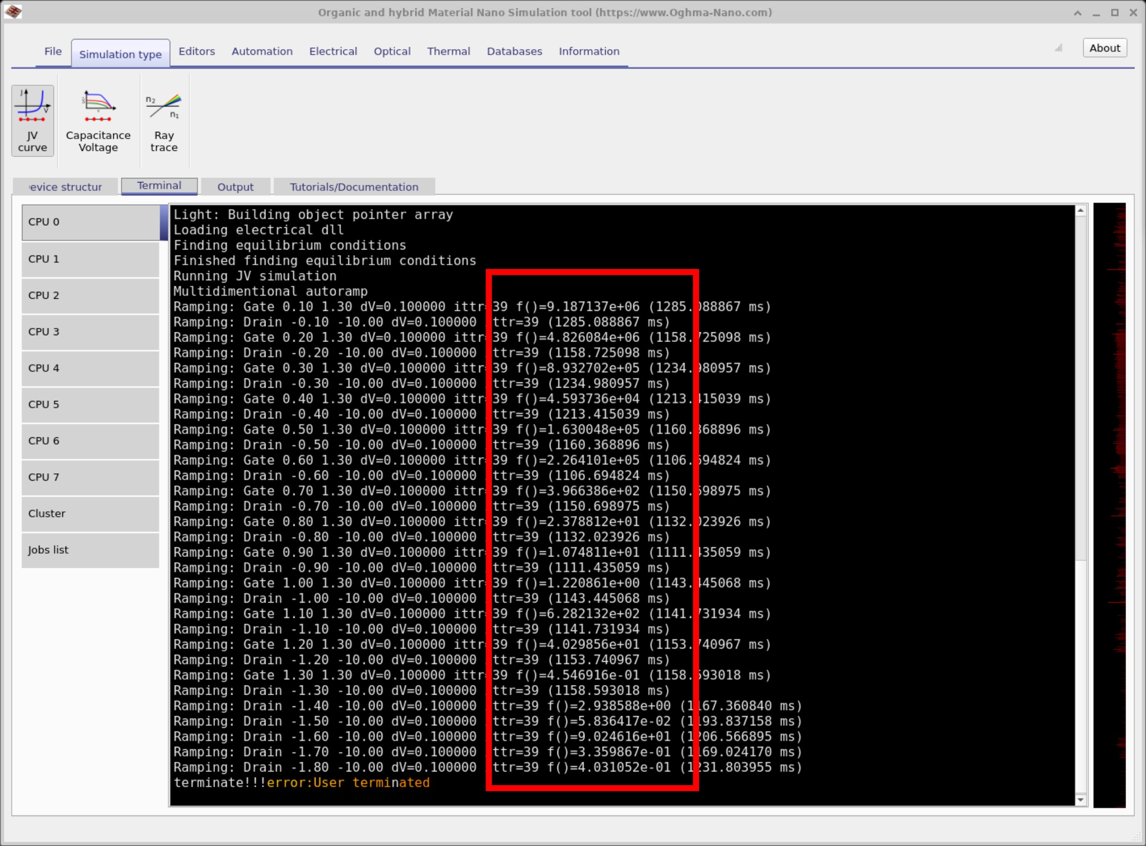
unnecessary numerical error. The figures below illustrate this: with 100 mesh points across the
device, the solver initially reports very large residuals (e.g. 1e6, 1e5). Only after
many iterations does it settle down to reasonable values of f(). This instability arises because the
mesh is excessively fine, making the system difficult for the solver to handle.
👉 Next steps:
- Return to the introduction to organic electronics for a broader overview of the topic.