OFET Electrical Parameters: Mobility, Traps, Permittivity and Contacts
This section explains how to configure OFET electrical parameters in OghmaNano, including carrier mobility, trap density, dielectric permittivity, recombination models and contact boundary conditions. These parameters determine how the drift–diffusion and Poisson equations are solved across the semiconductor and dielectric layers.
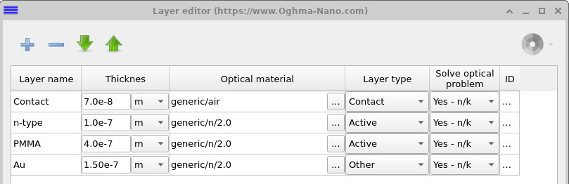
1. OFET layer editor: active layers, contacts and insulators
An OFET is built from a stack of layers, and you can edit their thicknesses in the Layer editor (Main window → Device structure tab). The editor allows you to view and modify the stack, add or remove layers, and assign a type to each one. OghmaNano supports three layer types:
- Contact layers — define the device terminals (e.g., source, drain, gate) and act as boundary conditions. They do not have electrical parameters, since their role is to set voltages or currents.
- Active layers — regions where the drift–diffusion and Poisson equations are solved. These layers carry charge and determine the electrical behaviour of the device. Only active layers appear in the Electrical parameters editor, where you can set mobilities, trap densities, permittivity, and related properties.
- Other layers — passive layers that are neither contacts nor electrically active. They may represent substrates, encapsulation, or optical spacers, and are ignored in the electrical solver.
In short, setting a layer to active tells OghmaNano to solve the drift–diffusion and Poisson equations across that region of the device. Contact layers remain fixed as boundary conditions, while other layers are structurally present but electrically inactive and excluded from the electrical solver.
2. Setting OFET electrical parameters
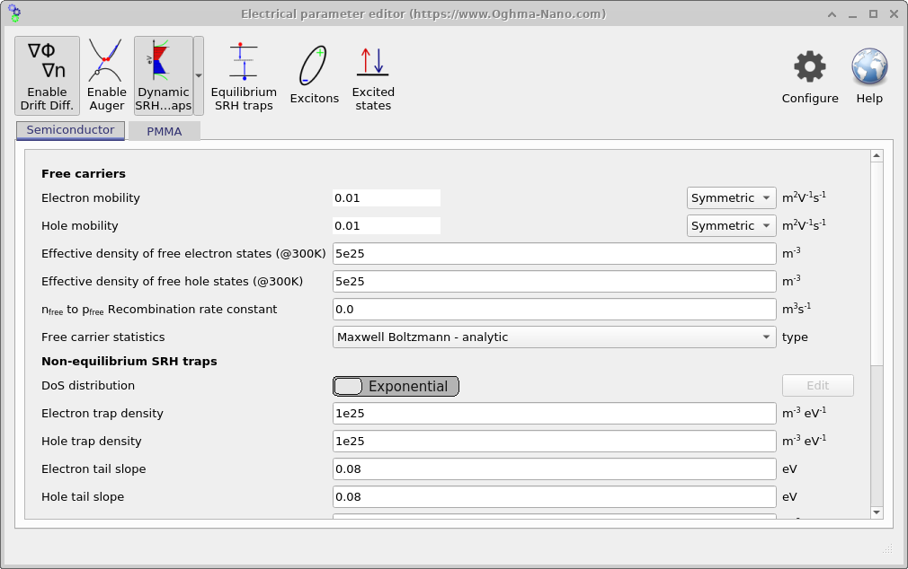
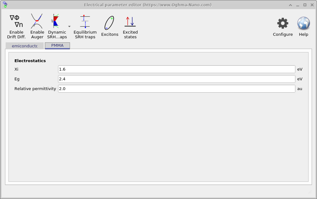
Once a layer has been marked as active in the Layer editor, its properties can be further defined in the Electrical Parameters editor. This is where you configure how charge transport, trapping, and electrostatics are modelled during simulation (see Section 3.1.9 for details). ?? shows the settings for the semiconducting layer, where you can specify mobilities, densities of states, trap parameters, and recombination models. ?? shows the corresponding settings for the PMMA insulator, where only electrostatic properties such as permittivity and band offsets are required. Notice the Enable Drift Diff. button at the top left: when enabled, the drift–diffusion equations are solved for that layer, including carrier motion. For the semiconductor this is switched on, since charge transport must be simulated, while for the PMMA insulator it is left off because the material does not conduct. Although it is possible to enable drift–diffusion everywhere and simply assign very low mobilities to insulating layers, this approach increases runtime and can reduce numerical stability. Disabling drift–diffusion in true insulators is therefore recommended.
3. Linking electrical parameters to OFET behaviour
The values entered in the Electrical Parameters editor directly control how the OFET behaves in simulation. For example, the semiconductor mobility determines the slope of the transfer curve, while the density of traps influences the subthreshold swing and hysteresis. The dielectric constant of the insulator sets the gate capacitance, which in turn controls how effectively the gate voltage modulates the channel. By experimenting with these parameters, you can explore how material properties translate into measurable device characteristics.
👉 Next steps:
- Continue to Part D to learn how mesh density, mobility values and solver settings affect OFET convergence and numerical stability.
- Return to the introduction to organic electronics for a broader overview of the topic.