Part B: Visualising the results from OFET simulations
To understand why an OFET behaves as it does, it is often necessary to go beyond external JV curves and examine the internal device state.
In OFET simulations, quantities such as electrostatic potential, charge-carrier density, trap occupancy and band energies provide direct insight
into how the transistor operates and how different regions contribute to performance. During each simulation, OghmaNano saves these internal
variables to the snapshots folder at every bias or time step. The Snapshots window can then be used to visualise these
results in 2D and 3D, allowing you to track how charge density, potential and other physical fields evolve with applied voltage.
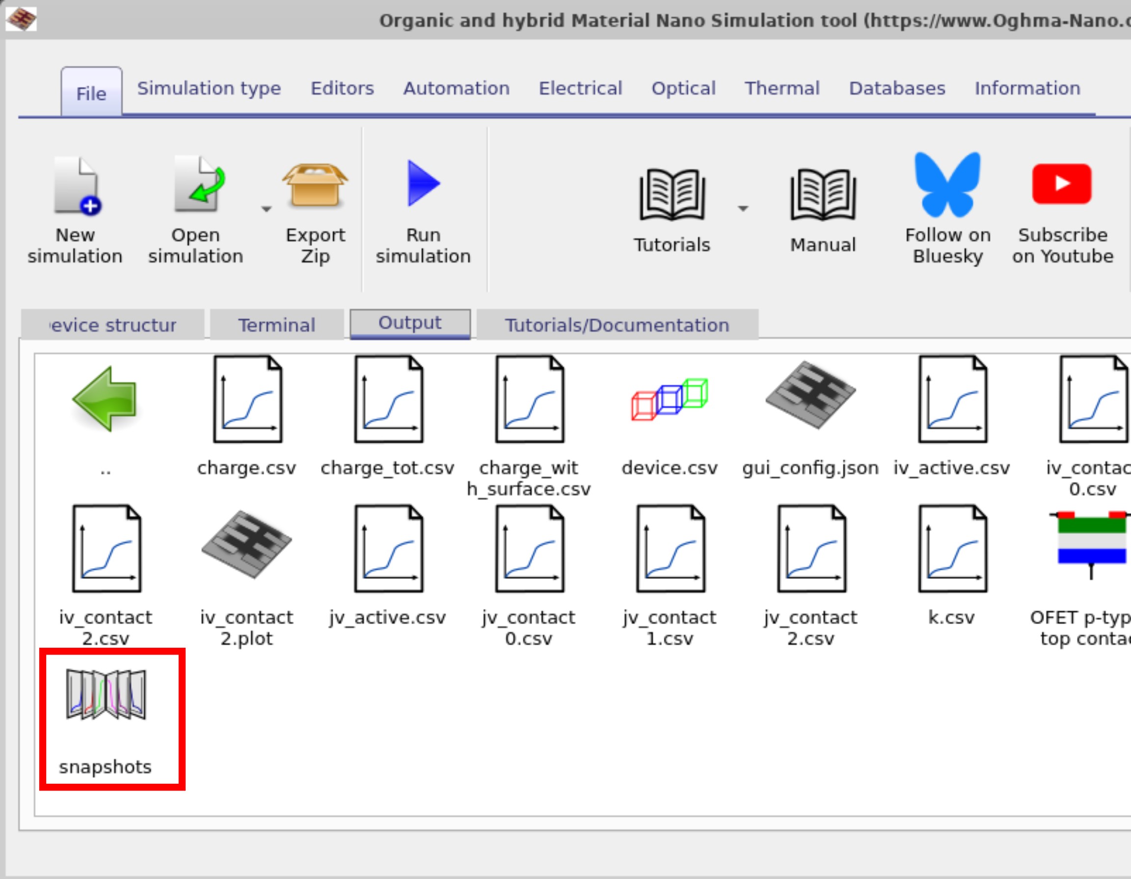
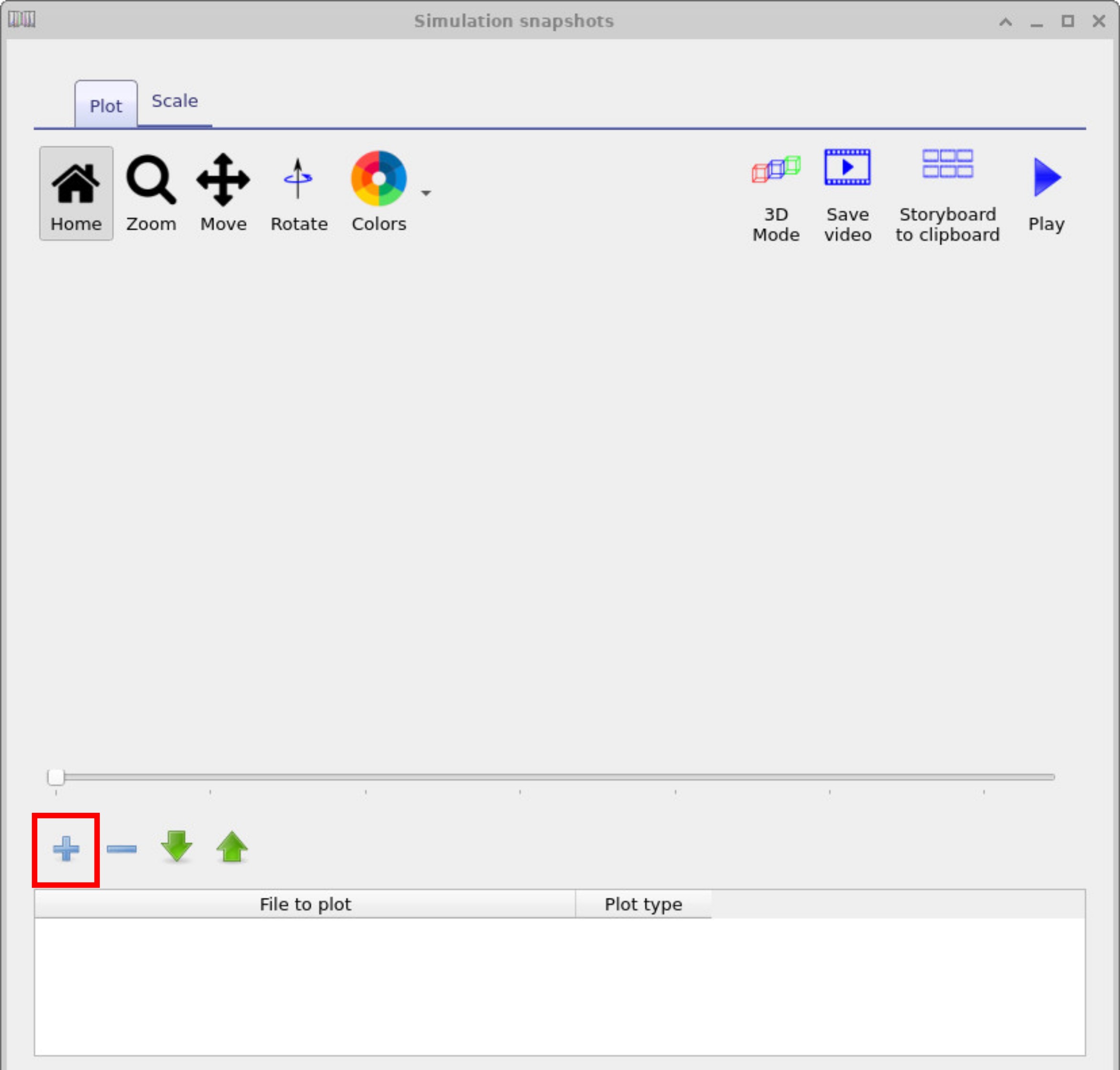
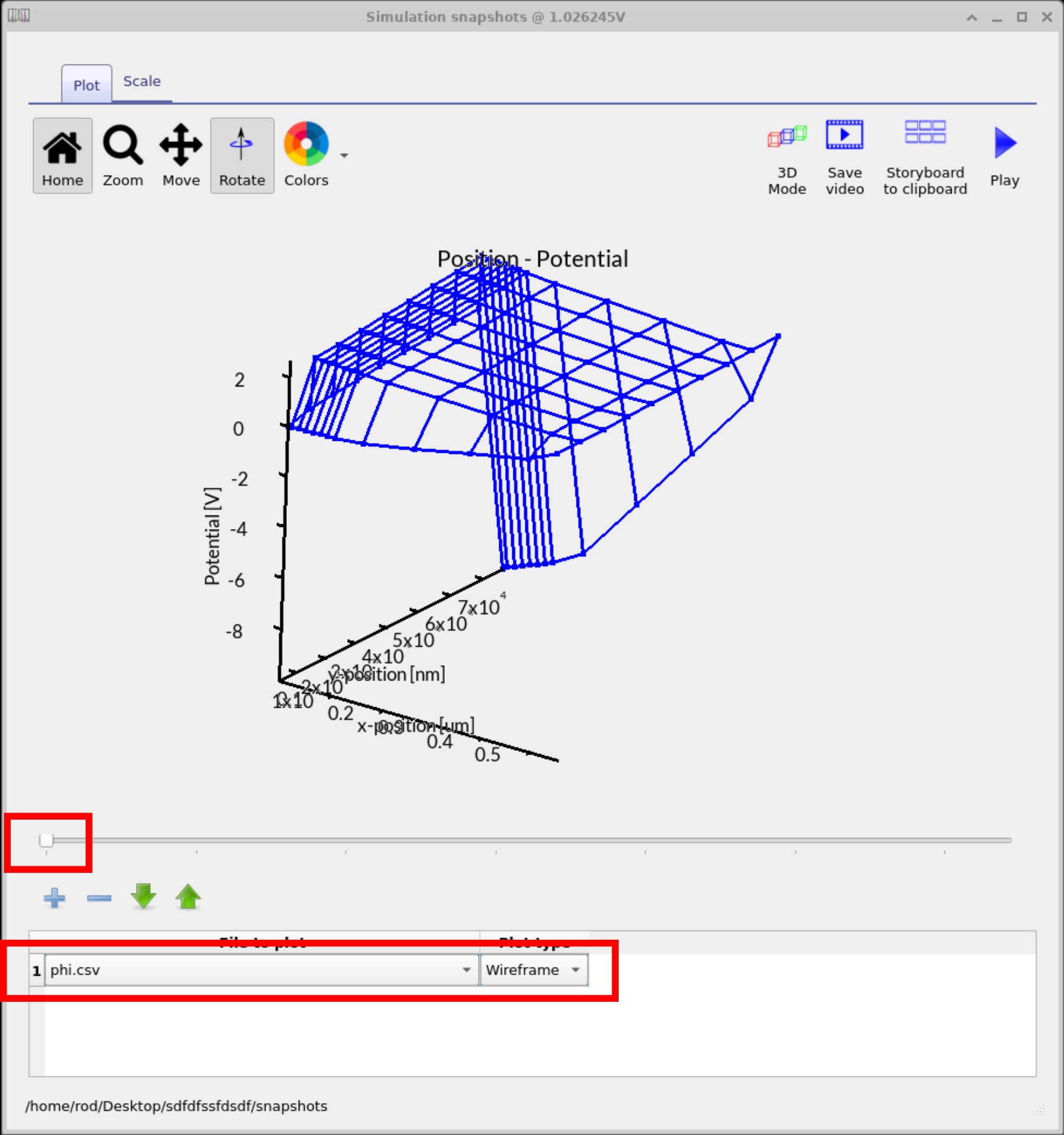
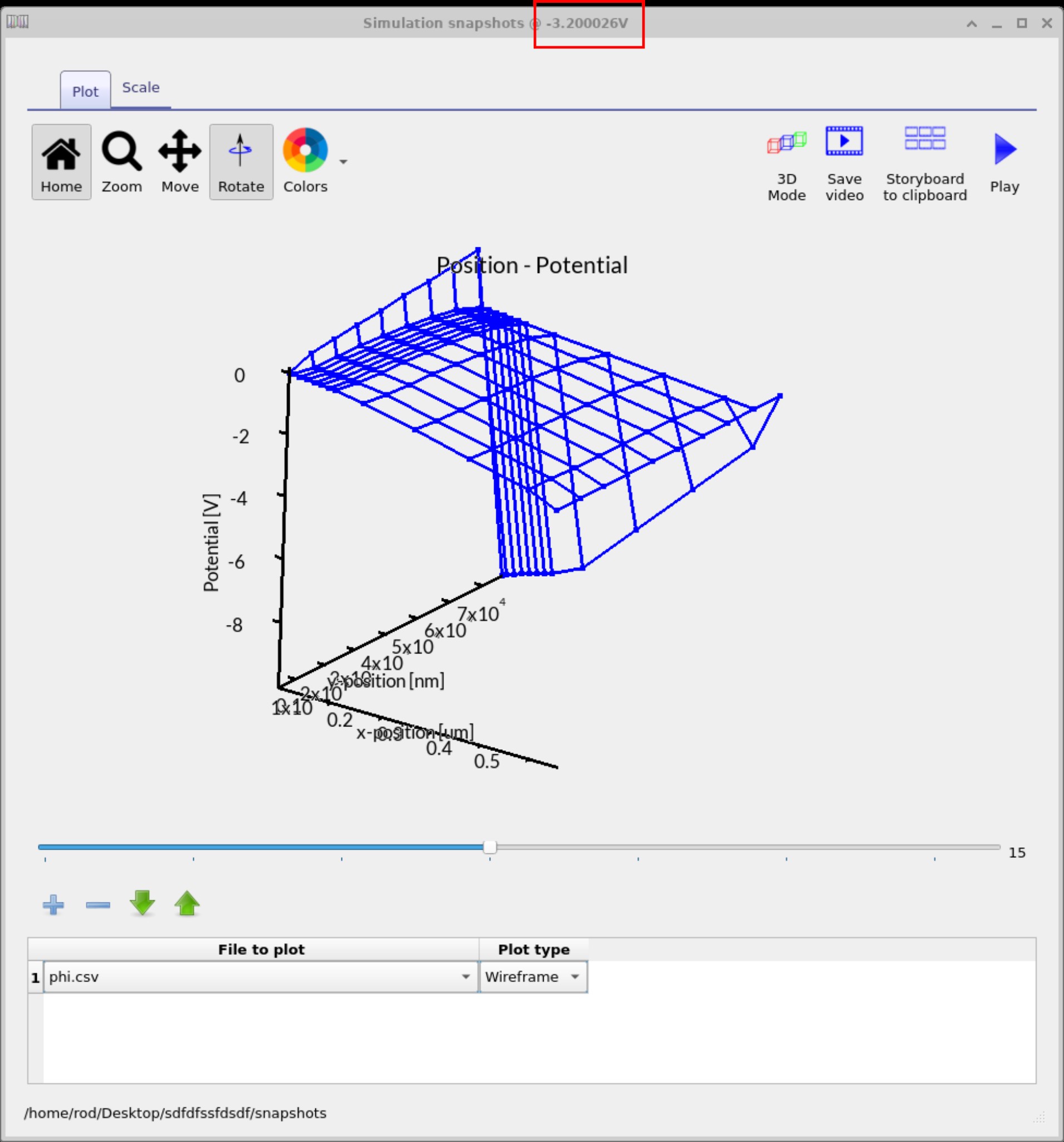
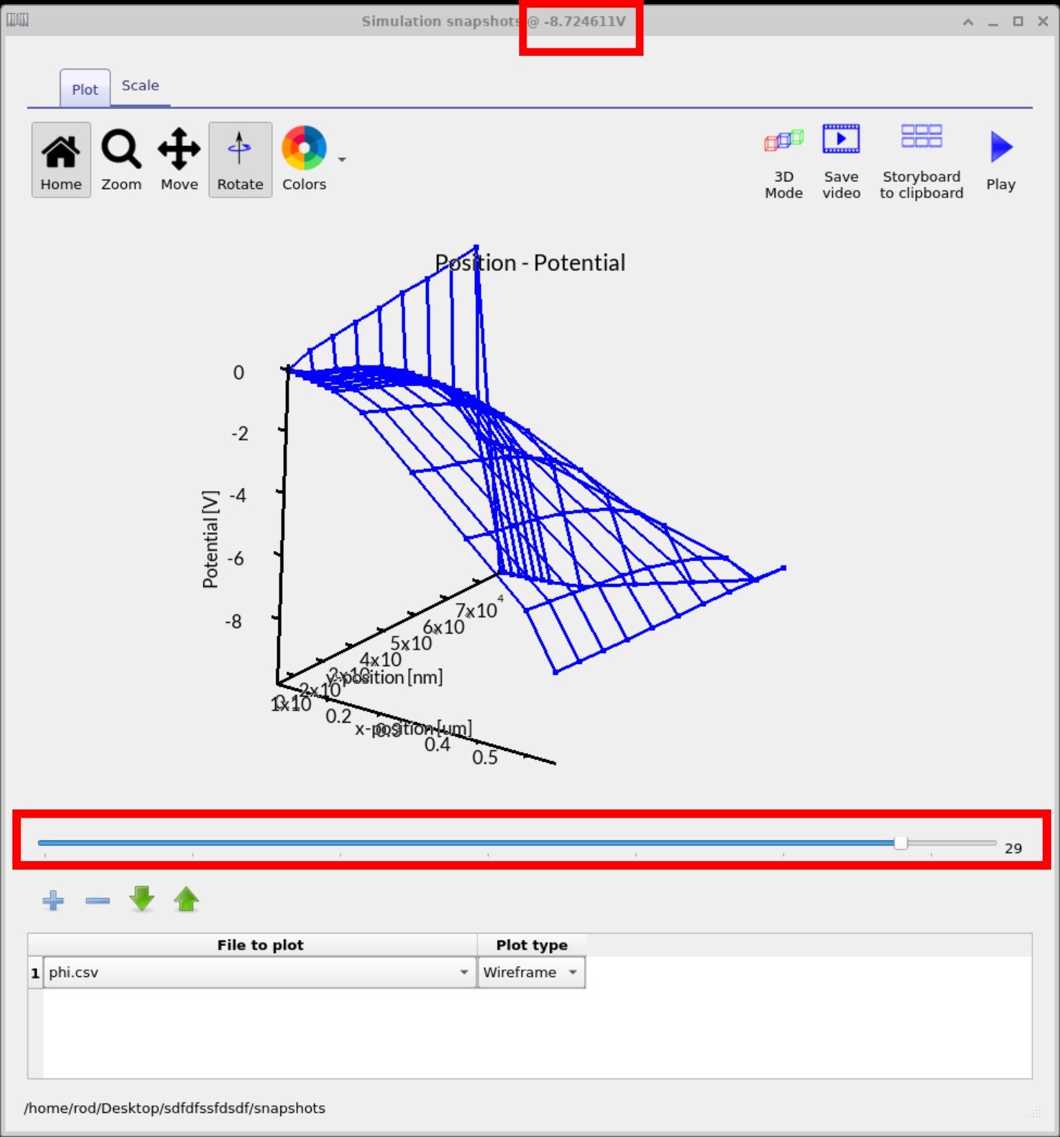
To visualise OFET simulation results in 2D or 3D, navigate to the Output tab in the main window and double-click the snapshots folder (??). This folder contains detailed internal data from the simulation, including charge-carrier density, electrostatic potential and trap occupancy across the device. Double-click the folder to open the Snapshots window (??), then click the + button to add a plot and select phy.csv from the drop-down menu. You can use the slider to step through bias points and render 2D fields such as charge density, trap density and electrostatic potential (φ), or switch to 3D mode to explore the full device. Use the mouse to rotate the view and the scroll wheel to zoom.
The figures ??, ??, ?? below show the evolution of the electrostatic potential (φ) across the OFET device at different applied voltages. Use the slider bar to view how internal fields change with bias. By selecting different variables from the drop-down menu, you can plot not only potential but also charge-carrier densities, trap occupancies, or other physical quantities to analyse how the device responds over the full voltage range.
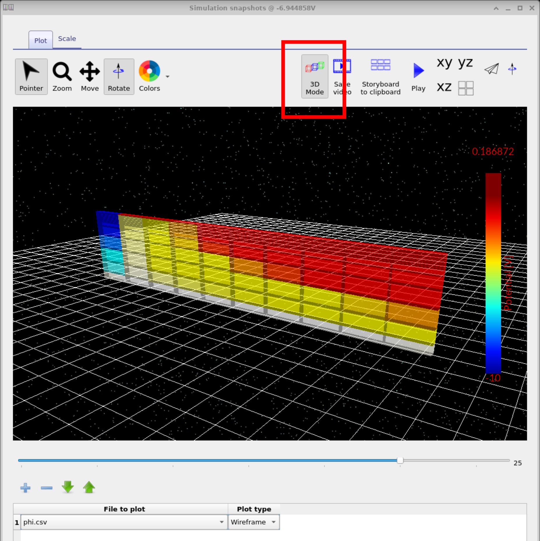
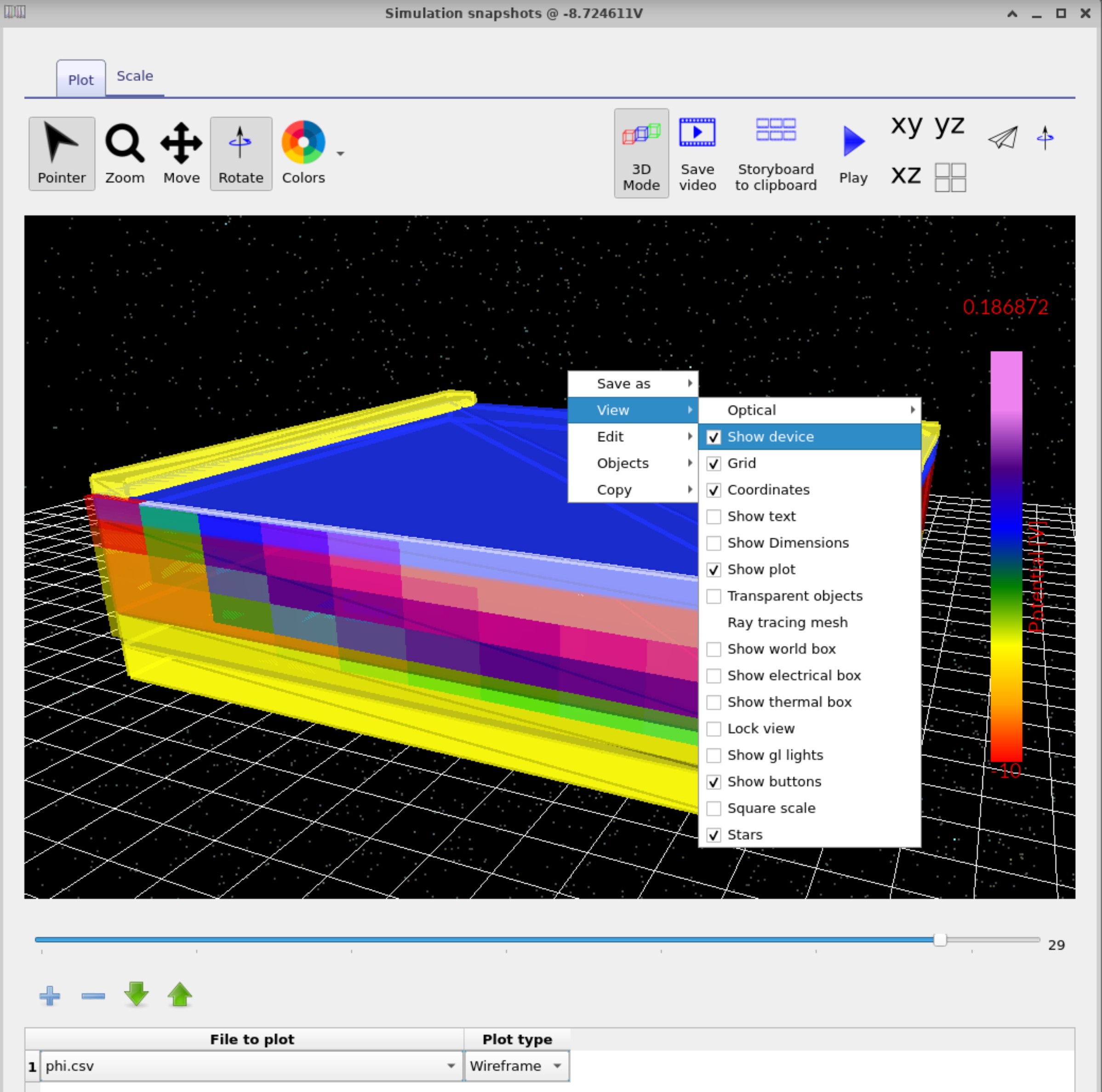
In addition to 2D mesh plots, OghmaNano also provides full 3D visualisation of simulation data. By pressing the 3D Mode button, the snapshots viewer flips from a flat mesh representation into a true 3D space (??). The user can still scroll through bias points with the slider to view how the data evolves, but now each field (such as electrostatic potential, φ) is mapped volumetrically across the device. In the second example (??), the colour map has been changed via the Colors button in the top ribbon, and the device itself has been made visible by right-clicking, selecting View → Show device. This combination of overlays makes it possible to directly relate the simulated physical fields (e.g. φ, charge density, traps) to the actual device geometry, providing a more intuitive understanding of how the device operates under bias.
👉 Next steps:
- Continue to Part C to learn how OFET electrical parameters such as mobility, trap density, permittivity and contacts affect the simulated device behaviour.
- Return to the introduction to organic electronics for a broader overview of the topic.