The parameter scan window
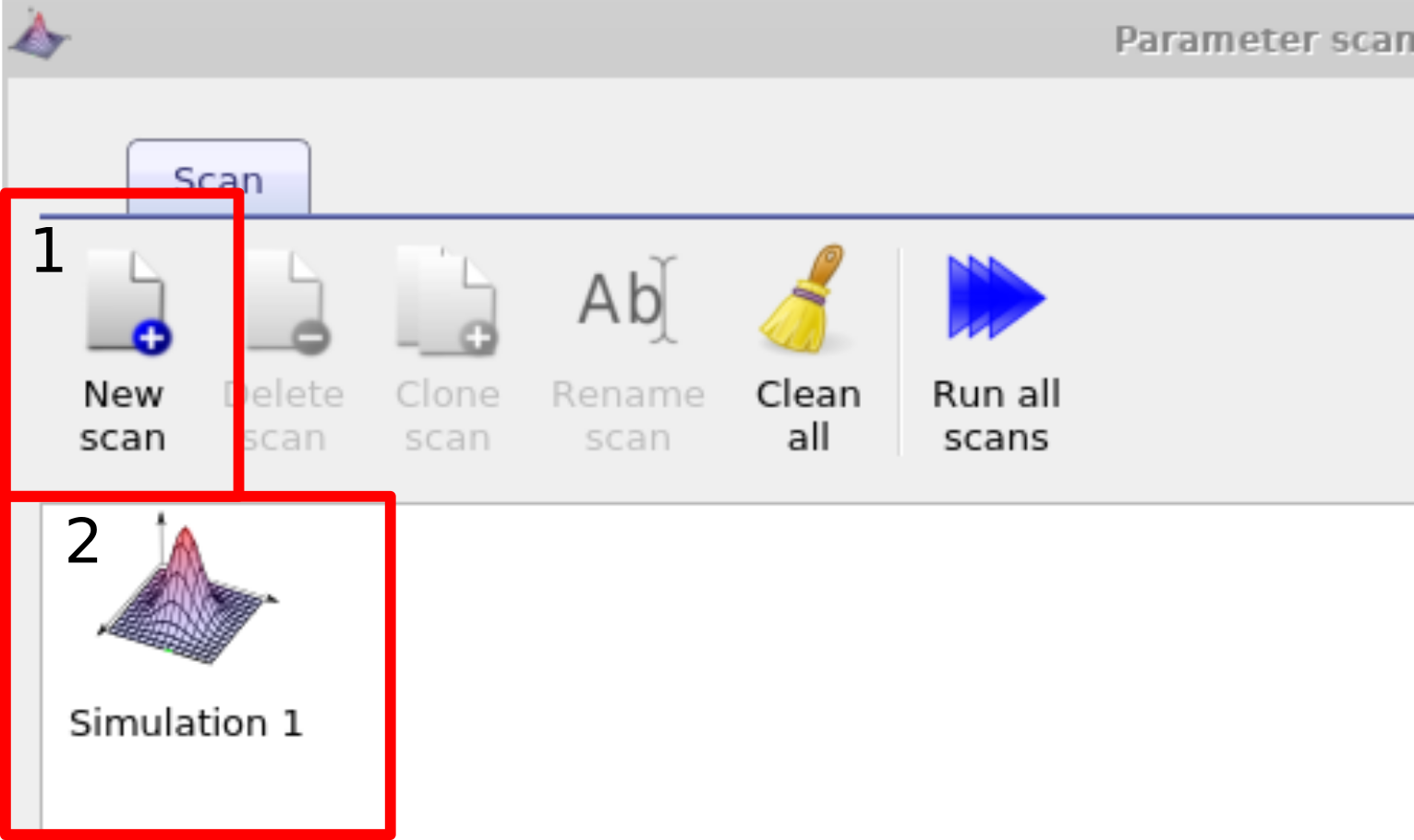
The most straightforward way to systematically vary a simulation parameter is to use the scan window. In this example we are going to systematically change the mobility of the active layer of a PM6:Y6 solar cell, you can find this example in the example simulations under Scripting and fitting/Scan demo (PM6:Y6 OPV). Once you have located this simulation and opened it, you then need to bring up the parameter scan window, this can be done by clicking on the Parameter scan icon in the Automation ribbon (see ??). Then make a new scan by clicking on the new scan button (1) (In the example simulation this has already been done for you). Open the new scan by double clicking on the icon representing the scan (2), see ??. This will bring up the scan window, see ??.
1. Selecting a parameter to vary
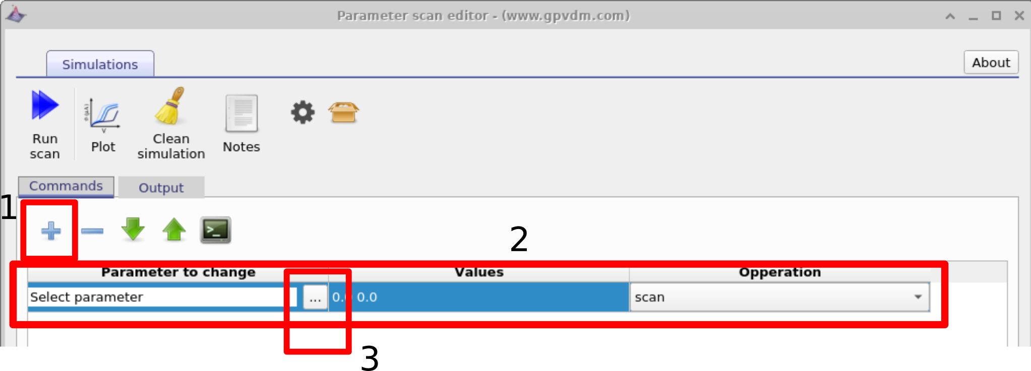
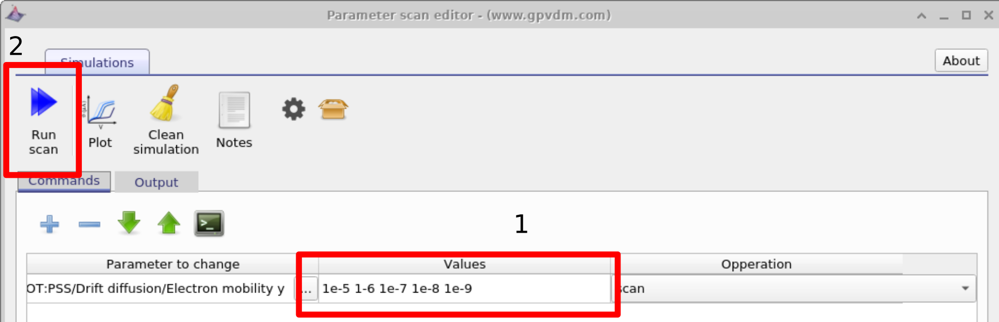
Once the scan window has opened, make a new scan line by clicking on the the plus icon (1) in figure 17.1, then select this line so that it is highlighted (2), then click on the three dots (3) to select which parameter you want to scan. Again if you are using the example simulation this will already have been done for you.
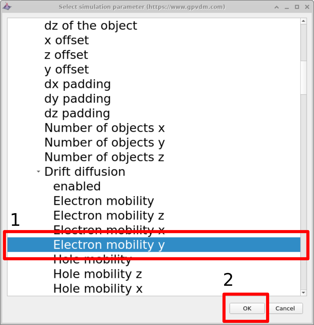
In this example, the electron mobility of a PM6:Y6 solar cell is selected for scanning. This is done by navigating to epitaxy\(\rightarrow\) PM6:Y6\(\rightarrow\) Drift diffusion\(\rightarrow\) Electron mobility y. Highlight the parameter and click OK. The selected parameter will then appear in the scan list. The meaning of each level in this parameter path is explained below:
-
epitaxy: All parameters defined in the
.oghmafile are exposed through the parameter selection window (see [fig:scanselect]). The overall device structure, including its layers, is defined under the epitaxy heading. -
PM6:Y6: Within epitaxy, each device layer is identified by name. In this example, the active layer is called PM6:Y6. If the active layer were named differently (for example Perovskite or P3HT:PCBM), that layer name would be selected instead.
-
Drift diffusion: All electrical transport parameters associated with a given layer are grouped under the drift diffusion subheading.
-
Electron mobility y: One can define asymmetric mobilities in the z,x and y direction - this is useful for OFET simulations. However by default the model assumes a symmetric mobility which is the same in all directions. This value is defined by Electron mobility y.
Although this workflow may appear relatively complex at first, it is essentially a structured way of
editing values and paths within the underlying .oghma JSON file.
The parameter selection window simply provides a graphical interface for navigating and modifying this
file safely and consistently.
A detailed description of the file structure can be found in the documentation at
the OghmaNano file format
.
2. Setting the values
Next enter the values of mobility which you want to scan over in this case we will be entering 1e-5 1-6 1e-7 1e-8 1e-9 then click run scan (see figure 17.2 2). OghmaNano will run one simulation on each core of your computer until all the simulations are finished.
3. Viewing the simulation results
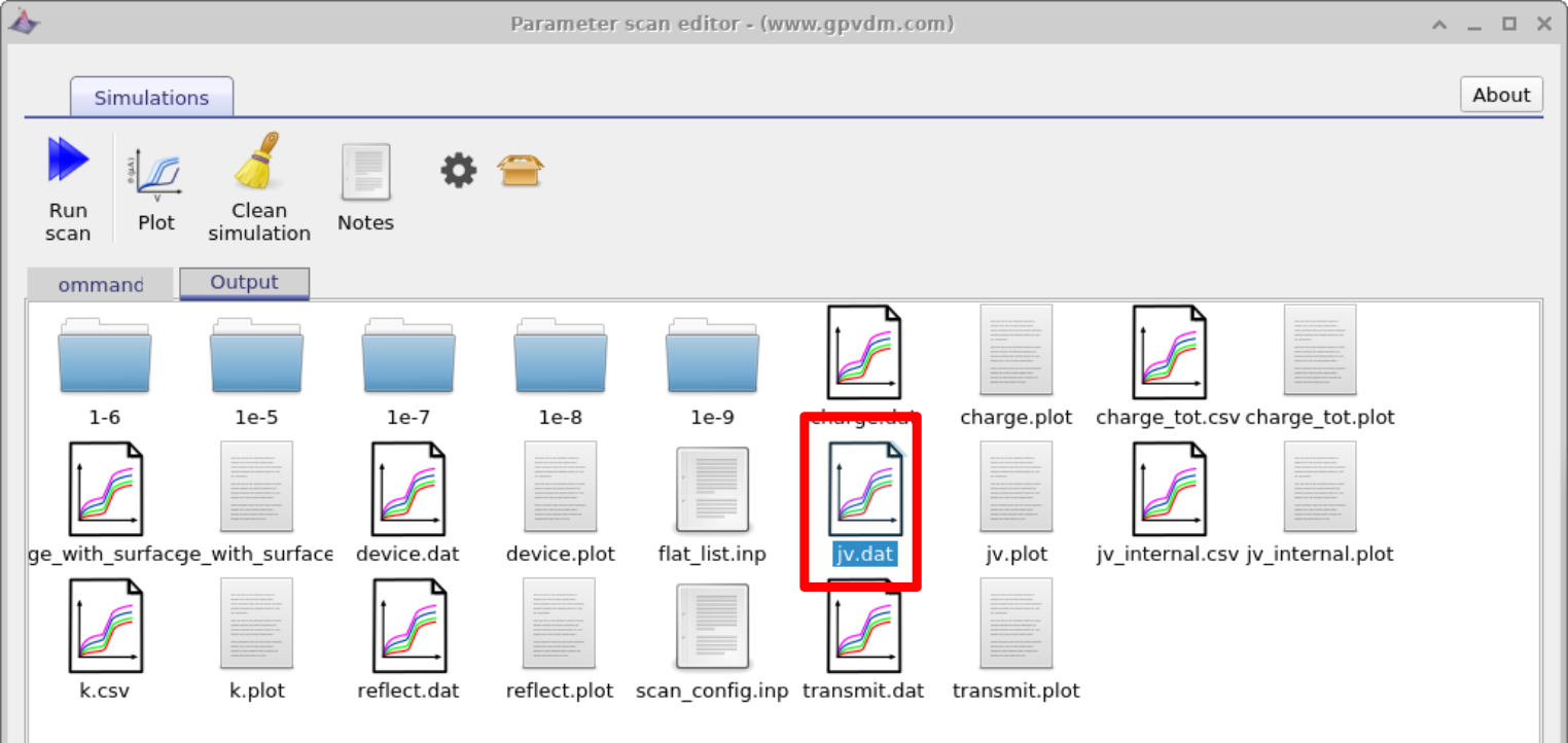
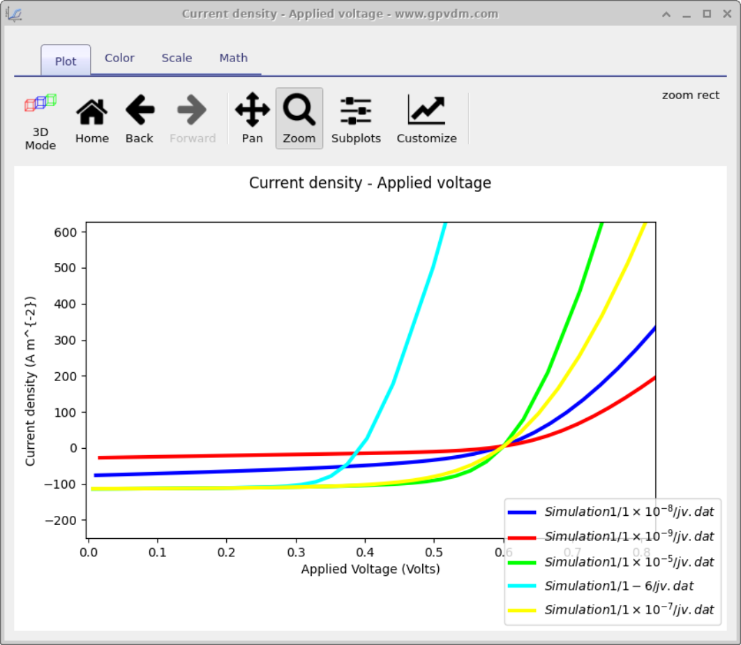
To view the simulation results click on the output tab this will bring up the simulation outputs, see figure 17.3. You can see that a directory has been created for each variable that we scanned over so 1e-5, 1e-6, 1e-7, 1e-8 and 1e-9. If you look inside each directory it will be an exact copy of the base simulation directory. If you double click on the files with multi-colored JV curves, see the red box in figure 17.3. OghmaNano will automaticity plot all the curves from each simulation in one graph, see figure 17.4.
4. Duplicating parameters – changing the thickness of the active layer
Very often, one wishes to vary a parameter and then set another parameter equal to the value that was changed. A simple example is scanning the electron and hole mobilities together when simulating a device with symmetric transport properties. This can be achieved using the Duplicate function of the scan window, as shown in ??. In this example, we consider a slightly more subtle problem. Rather than duplicating mobilities, we change the physical thickness of the active layer and, at the same time, adjust the electrical mesh so that it matches. As discussed in the meshing section, the width of the active layer should match the width of the electrical mesh. It is better if these are kept consistent to avoid numerical and geometric inconsistencies in the simulation.
When the layer width is changed manually in the layer editor, OghmaNano automatically updates the electrical mesh. However, when the model is modified via scripting or parameter scans, this update may not be performed automatically. Therefore, in the example below, we explicitly duplicate the relevant parameters.
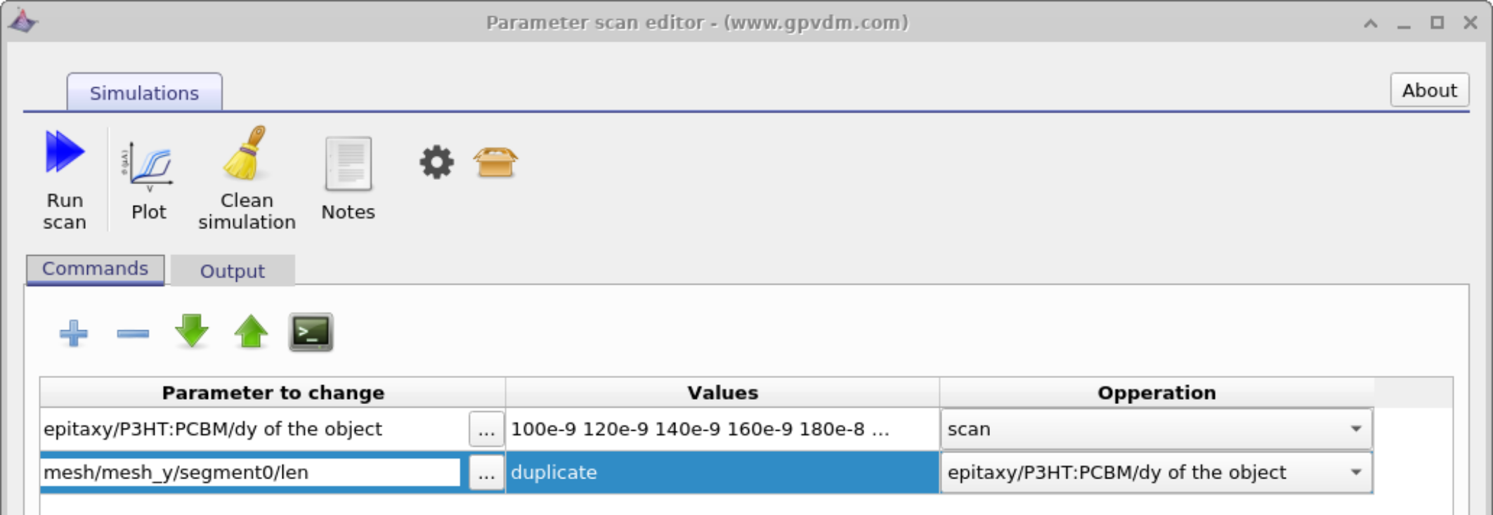
First, we scan over:
epitaxy\(\rightarrow\)PM6:Y6\(\rightarrow\)dy of the object
Next, we add another scan line and, under Parameter to scan, select:
mesh\(\rightarrow\)mesh_y\(\rightarrow\)segment0\(\rightarrow\)len
This parameter is then set to:
epitaxy\(\rightarrow\)PM6:Y6\(\rightarrow\)dy of the object
using the Operation dropdown menu. Once selected, the word duplicate will appear under the Values column.
When the simulation is run, the parameter “epitaxy\(\rightarrow\)PM6:Y6\(\rightarrow\)dy of the object” is scanned, and “mesh\(\rightarrow\)mesh_y\(\rightarrow\)segment0\(\rightarrow\)len” automatically follows it, ensuring that the mesh thickness remains consistent with the physical layer thickness.
5. Setting constant values
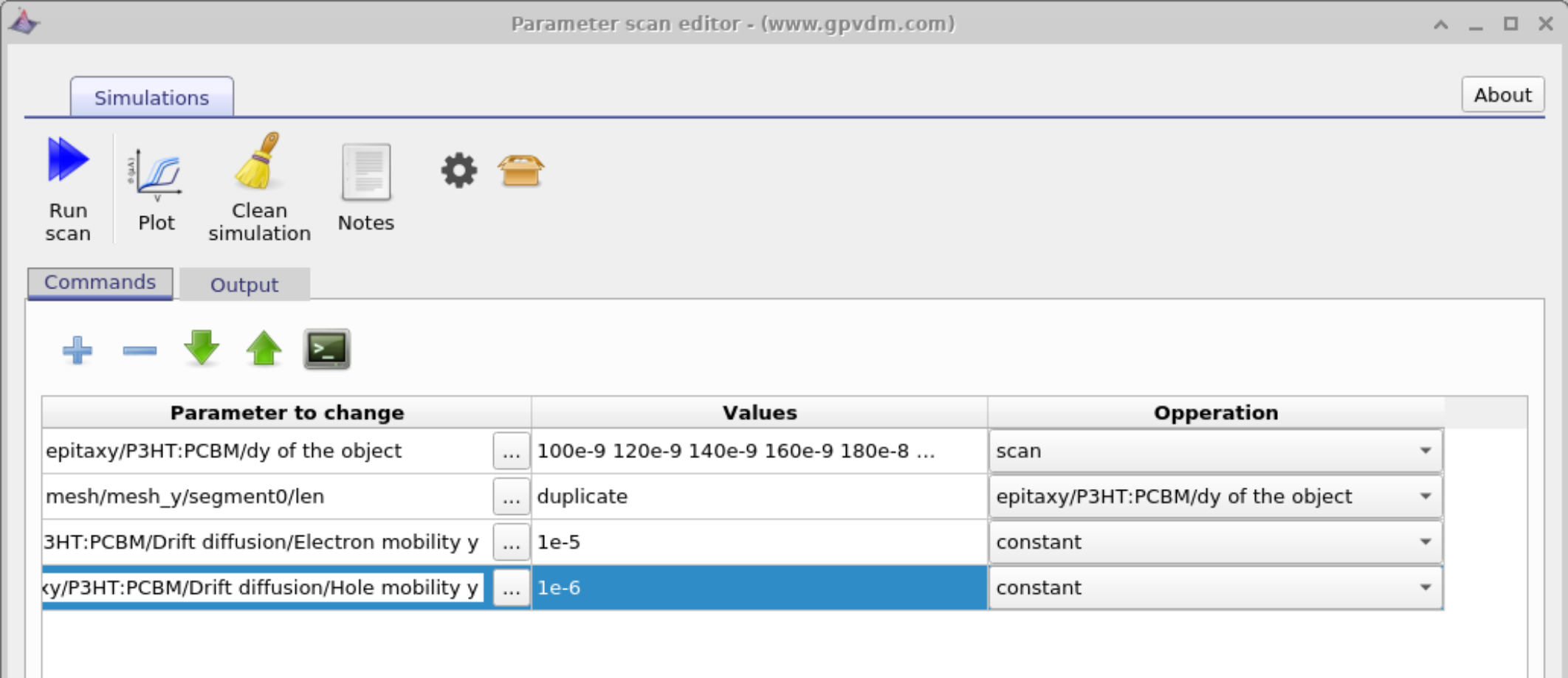
In addition to scanning parameters, the parameter scan editor can be used to explicitly set parameters to fixed values using the constant operation. This is useful when several parameters must remain unchanged while another parameter is being varied.
In this example, the thickness of the active layer is varied by scanning the dy parameter of the device layer. At the same time, the corresponding vertical mesh segment length is duplicated so that the electrical mesh remains consistent with the changing layer thickness. Alongside these scanned parameters, both the electron mobility and hole mobility are set to fixed values using the constant option in the Operation column.
Using constant ensures that these parameters take the specified value for every simulation in the scan, regardless of how other parameters change. This makes it possible to cleanly separate the effect of geometry changes (such as layer thickness) from transport parameters, and avoids unintended coupling between scanned quantities.
6. The equivalent of loops
When scanning over a parameter range, it is often desirable to run a large number of simulations. In such cases, manually entering every value is impractical. To address this, OghmaNano provides the equivalent of a loop within the scan window.
For example, to vary a parameter from 100 to 400 in steps of 1, you can enter:
[100 400 1]
7. Limitations of the scan window
The scan window provides a pragmatic and easy way to vary a material or device parameter and quickly visualise the results. For simple studies-where the goal is to understand how a quantity changes and to obtain results within seconds-it is often the most effective approach.
However, once the number of simulations becomes large, or when more complex parameter interactions are required, the scan window can become limiting. In such cases, it may be more appropriate to drive OghmaNano programmatically using a scripting interface, for example via Python or MATLAB, which allow full control over parameter generation, execution logic, and data collection.
Similarly, if the objective is to optimise a device stack-rather than simply observe how curves vary with a parameter-it is usually better to use the built-in optimisation tools. These are described in the multiparameter device optimizer section of the manual.
👉 Next step: Now continue to Multiparameter Optimization, where you can learn how to optimize several device parameters simultaneously.