

Theory of the transfer matrix method
1. Introduction
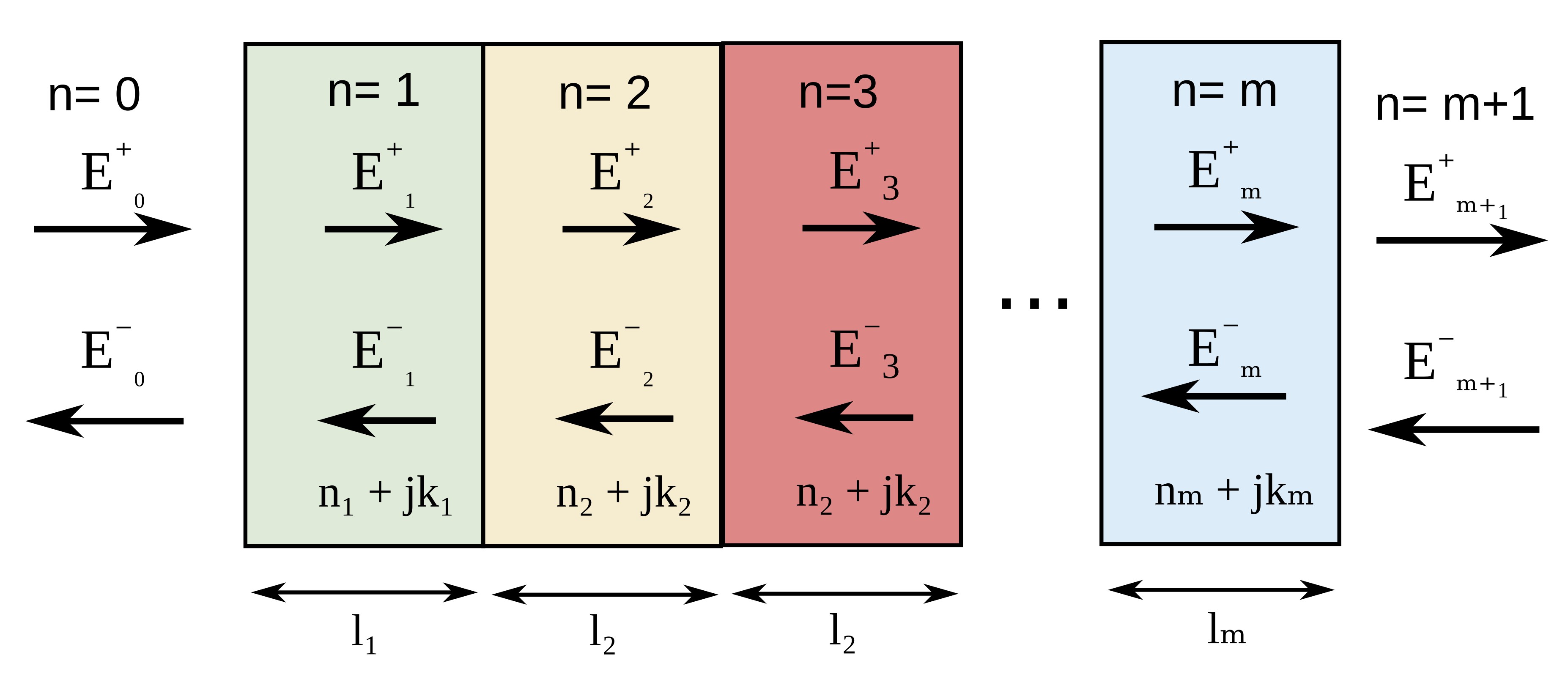
On this page we derive the transfer matrix method (TMM) for multilayer dielectric structures, as shown in figure ??. Such layered structures resemble the optical stacks found in OLEDs, thin-film solar cells and optical coatings, where the individual layer thicknesses are comparable to the wavelength of light, typically ranging from hundreds of nanometres to several microns. Under these conditions, optical interference, reflection and absorption strongly influence device performance and must therefore be treated using Maxwell’s equations and wave optics rather than simple ray optics. For a broader introduction to the transfer matrix method and its applications in optical modelling, see What is the transfer matrix method?. For a practical step-by-step guide showing how to use the optical transfer matrix model in OghmaNano, see Optical transfer matrix model.
2. Derivation
Considering the interface between layers 1 and 2 in figure ??, the electric field on the left-hand side of the interface is given by
\begin{equation} E_{1}=E^{+}_{1} e^{-j k_1 z}+E^{-}_{1} e^{j k_1 z} \label{eq:efield1} \end{equation}and on the right-hand side of the interface the electric field is given by
\begin{equation} E_{2}=E^{+}_{2} e^{-j k_2 z}+E^{-}_{2} e^{j k_2 z} \label{eq:efield2} \end{equation}Maxwell’s equations give the relationship between the electric and magnetic fields for a plane wave,
\begin{equation} \nabla \times \mathbf{E}=-j\omega \mu \mathbf{H} \end{equation}which in one dimension simplifies to
\begin{equation} \frac{\partial E} {\partial z}=-j\omega \mu H \label{eq:maxwell} \end{equation}Applying equation \eqref{eq:maxwell} to equations \eqref{eq:efield1} and \eqref{eq:efield2}, we obtain the magnetic field on the left-hand side of the interface
\begin{equation} -j \mu \omega H^{y}_{1}=-j k_1 E^{+}_{1} e^{-j k_1 z}+j k_1 E^{-}_{1} e^{j k_1 z} \end{equation}and on the right-hand side of the interface
\begin{equation} -j \mu \omega H^{y}_{2}=-j k_2 E^{+}_{2} e^{-j k_2 z}+j k_2 E^{-}_{2} e^{j k_2 z} \end{equation}Tidying up gives,
\begin{equation} H^{y}_{1}=\frac{k_1}{\omega \mu}E^{+}_{1} e^{-j k_1 z}-\frac{k_1}{\omega \mu} E^{-}_{1} e^{j k_1 z} \end{equation} \begin{equation} H^{y}_{2}=\frac{k_2}{\omega \mu}E^{+}_{2} e^{-j k_2 z}-\frac{k_2}{\omega \mu} E^{-}_{2} e^{j k_2 z} \end{equation}3. Boundary conditions
We now apply the electric and magnetic boundary conditions
\begin{equation} \mathbf{n} \times (\mathbf{E_2}-\mathbf{E_1})=0 \end{equation} \begin{equation} \mathbf{n} \times (\mathbf{H_2}-\mathbf{H_1})=0 \end{equation}Evaluating the fields at the interface \(z=0\) gives
\begin{equation} (E_{2}^{+}+E_{2}^{-})-(E_{1}^{+}+E_{1}^{-})=0 \label{eq:electric_boundary} \end{equation}and
\begin{equation} \frac{k_2}{\omega \mu}(E_{2}^{+}-E_{2}^{-}) - \frac{k_1}{\omega \mu}(E_{1}^{+}-E_{1}^{-})=0 \end{equation}The wavevector is given by
\begin{equation} k=\frac{2\pi n}{\lambda} \end{equation}We can therefore write the magnetic boundary condition as
\begin{equation} n_2 (E_{2}^{+}-E_{2}^{-}) - n_1 (E_{1}^{+}-E_{1}^{-})=0 \label{eq:mag_boundary} \end{equation}4. Forward propagating wave
Rearranging equation \eqref{eq:mag_boundary} gives
\begin{equation} E_{1}^{-} = E_{1}^{+} - \frac{n_2}{n_1}(E_{2}^{+}-E_{2}^{-}) \end{equation}Substituting into equation \eqref{eq:electric_boundary} gives
\begin{equation} E_{2}^{+}+E_{2}^{-} = E_{1}^{+}+E_{1}^{+} - \frac{n_2}{n_1}(E_{2}^{+}-E_{2}^{-}) \end{equation} \begin{equation} 2E_{1}^{+} = E_{2}^{+}+E_{2}^{-} + \frac{n_2}{n_1}(E_{2}^{+}-E_{2}^{-}) \end{equation} \begin{equation} 2E_{1}^{+}\frac{n_1}{n_1+n_2} = E_{2}^{+} + E_{2}^{-}\frac{n_1-n_2}{n_1+n_2} \end{equation}5. Backwards propagating wave
Rearrange equation \eqref{eq:mag_boundary} to give,
\begin{equation} E_{1}^{+}=E_{1}^{-} +\frac{n_2}{n_1}(E_{2}^{+}-E_{2}^{-}) \end{equation}Inserting in equation \eqref{eq:electric_boundary}, gives
\begin{equation} E_{2}^{+}+E_{2}^{-}=E_{1}^{-} +\frac{n_2}{n_1}(E_{2}^{+}-E_{2}^{-})+E_{1}^{-} \end{equation} \begin{equation} 2E_{1}^{-}=E_{2}^{+}+E_{2}^{-}- \frac{n_2}{n_1}(E_{2}^{+}-E_{2}^{-}) \end{equation} \begin{equation} 2E_{1}^{-}\frac{n_1}{n_1+n_2}=E_{2}^{+}\frac{n_1-n_2}{n_1+n_2}+E_{2}^{-} \end{equation}These equations become:
\begin{equation} E_{1}^{-}t_{12}=E_{2}^{+}r_{12}+E_{2}^{-} \end{equation}and
\begin{equation} E_{1}^{+}t_{12}=E_{2}^{+}+E_{2}^{-}r_{12} \end{equation}Accounting for propagation we can write.
\begin{equation} E_{1}^{+}t_{12}=E_{2}^{+}e^{\zeta_2 d_1}+E_{2}^{-}r_{12}e^{-\zeta_2 d_1} \end{equation}and
\begin{equation} E_{1}^{-}t_{12}=E_{2}^{+}r_{12}e^{\zeta_2 d_1}+E_{2}^{-}e^{-\zeta_2 d_1} \end{equation}where
\begin{equation} \zeta=\frac{2\pi}{\lambda} \bar{n} \end{equation}6. Transfer matrix implementation
The transfer matrix method can now be implemented by writing the optical fields in each layer as a vector containing the forward and backward propagating waves. The multilayer optical stack is then solved by repeatedly multiplying small matrices describing propagation through each layer and reflection/transmission at each interface. This approach is computationally efficient and only requires simple matrix multiplication operations, making it straightforward to implement numerically.
The optical field in layer \(i\) is written as
\begin{equation} \begin{pmatrix} E_i^{+} \\ E_i^{-} \end{pmatrix} \end{equation}where \(E_i^{+}\) and \(E_i^{-}\) are the forward and backward propagating waves respectively.
At each interface the Fresnel reflection and transmission coefficients are given by
\begin{equation} r_{ij}=\frac{n_i-n_j}{n_i+n_j}, \qquad t_{ij}=\frac{2n_i}{n_i+n_j} \end{equation}The interface between layers \(i\) and \(j\) can therefore be written as
\begin{equation} \begin{pmatrix} E_i^{+} \\ E_i^{-} \end{pmatrix} = \frac{1}{t_{ij}} \begin{pmatrix} 1 & r_{ij} \\ r_{ij} & 1 \end{pmatrix} \begin{pmatrix} E_j^{+} \\ E_j^{-} \end{pmatrix} \end{equation}Propagation through a layer of thickness \(d_i\) is described by
\begin{equation} \begin{pmatrix} E_i^{+}(z+d_i) \\ E_i^{-}(z+d_i) \end{pmatrix} = \begin{pmatrix} e^{\zeta_i d_i} & 0 \\ 0 & e^{-\zeta_i d_i} \end{pmatrix} \begin{pmatrix} E_i^{+}(z) \\ E_i^{-}(z) \end{pmatrix} \end{equation}where
\begin{equation} \zeta_i=\frac{2\pi \bar{n}_i}{\lambda} \end{equation}The transfer matrix for a single layer is obtained by multiplying the interface and propagation matrices together
\begin{equation} M_i= \frac{1}{t_{ij}} \begin{pmatrix} 1 & r_{ij} \\ r_{ij} & 1 \end{pmatrix} \begin{pmatrix} e^{\zeta_i d_i} & 0 \\ 0 & e^{-\zeta_i d_i} \end{pmatrix} \end{equation}The optical response of the full multilayer device is then obtained by multiplying the matrices together
\begin{equation} M=M_1M_2M_3 \cdots M_n \end{equation}such that
\begin{equation} \begin{pmatrix} E_0^{+} \\ E_0^{-} \end{pmatrix} = M \begin{pmatrix} E_n^{+} \\ E_n^{-} \end{pmatrix} \end{equation}For a device with no incoming wave from the rear contact, \(E_n^{-}=0\). The reflected and transmitted fields can then be calculated directly from the resulting matrix elements.
7. Solving in One Large Matrix
The derivation above describes the classical transfer matrix method, where the optical field is propagated through a sequence of discrete layers using transfer matrices. This approach is highly efficient and works extremely well for conventional multilayer structures such as solar cells, OLEDs, optical filters, and thin-film sensors, where the device can be naturally described as a stack of well-defined layers.
In some optical systems, however, the geometry does not lend itself to a simple layered description. Examples include graded-index structures, devices containing air gaps, distributed feedback (DFB) gratings, and three-dimensional structures projected onto a one-dimensional optical mesh. In these situations it can become cumbersome to represent the system as a sequence of discrete layers with well-defined interfaces.
To address this problem, OghmaNano can project the transfer matrix equations onto a finite-difference mesh. Rather than propagating the optical field layer-by-layer, the entire optical system is represented by a single matrix containing all forward- and backward-propagating wave components simultaneously. The resulting linear system is then solved in a single matrix inversion.
For a device with non-reflecting back contacts, the resulting system takes the form:
\begin{equation} \begin{pmatrix} e^{\zeta d} & 0 & 0 & 0 & r_{01}e^{-\zeta d} & 0 & 0 & 0 \\ -t_{12} & e^{\zeta d} & 0 & 0 & 0 & r_{12}e^{-\zeta d} & 0 & 0 \\ 0 & -t_{23} & e^{\zeta d} & 0 & 0 & 0 & r_{23}e^{-\zeta d} & 0 \\ 0 & 0 & -t_{34} & e^{\zeta d} & 0 & 0 & 0 & r_{34}e^{-\zeta d} \\ 0 & r_{12}e^{\zeta d_1} & 0 & 0 & -t_{12} & e^{-\zeta d} & 0 & 0 \\ 0 & 0 & r_{23}e^{\zeta d} & 0 & 0 & -t_{23} & e^{-\zeta d} & 0 \\ 0 & 0 & 0 & r_{34}e^{\zeta d} & 0 & 0 & -t_{34} & e^{-\zeta d} \\ 0 & 0 & 0 & 0 & 0 & 0 & 0 & -t_{45} \end{pmatrix} \begin{pmatrix} E_{1}^{+} \\ E_{2}^{+} \\ E_{3}^{+} \\ E_{4}^{+} \\ E_{1}^{-} \\ E_{2}^{-} \\ E_{3}^{-} \\ E_{4}^{-} \end{pmatrix} = \begin{pmatrix} t_{01}E_{external} \\ 0 \\ 0 \\ 0 \\ 0 \\ 0 \end{pmatrix} \end{equation}The unknown vector contains the forward- and backward-propagating optical fields throughout the device, while the coefficient matrix contains the transmission and reflection relationships between neighbouring mesh points or interfaces. The right-hand-side vector represents the externally incident optical field.
For conventional multilayer devices, the finite-difference formulation generally produces results that are very similar to those obtained using the classical transfer matrix method. The main advantage of the approach is its flexibility: complex geometries can be represented directly on a mesh without first converting them into a sequence of idealised layers. This makes the method particularly useful for structures such as DFB gratings, graded-index devices, and other optical systems where the material properties vary continuously through space.
From the user's perspective the classical transfer matrix and finite-difference formulations produce similar outputs, including photon density, absorbed photon density, reflection, transmission, and generation profiles. The choice between the two methods is therefore primarily determined by how naturally the optical structure can be represented.
8. Complex refractive index and optical absorption
Optical absorption in the transfer matrix method is included through the complex refractive index \(n+j\kappa\), where \(n\) is the refractive index and \(\kappa\) is the extinction coefficient. The electric field propagating through an absorbing medium is given by
\begin{equation} E(z,t)=Re(E_0 e^{j(-kz+\omega t)})= Re(E_0 e^{j(\frac{-2 \pi (n+j\kappa)}{\lambda}z + \omega t)})=e^{\frac{2\pi\kappa z}{\lambda}}Re(E_0 e^{\frac{j(-2 \pi (n+j\kappa)}{\lambda}z +\omega t}) \end{equation}Because the optical intensity is proportional to the square of the electric field, the absorption coefficient becomes
\begin{equation} e^{-\alpha x}=e^{\frac{2\pi\kappa z}{\lambda}} \end{equation} \begin{equation} \alpha=-\frac{4\pi\kappa}{\lambda_0} \end{equation}👉 Next step: Continue to the Transfer Matrix simulation tool to learn how TMM is implemented inside OghmaNano.