Transfer matrix model (TMM)
1. Introduction
The transfer matrix method (TMM) is a fast, reliable technique for modeling light propagation in multilayer (“sandwich-type”) structures under normal incidence. It is widely used for devices such as solar cells, optical filters, OLEDs, and optical sensors, where you need to quantify how light is absorbed, reflected, and transmitted through thin films. If you are new to the technique, see What is the Transfer Matrix Method?. A more detailed mathematical treatment is given in Derivation of the Transfer Matrix Method.
Compared with full-wave solvers such as FDTD (Finite-Difference Time-Domain), TMM achieves similar insights at a computational cost that is typically orders of magnitude lower. This makes it ideal for rapid design iteration, parameter sweeps, and optimization of multilayer stacks, while still capturing the key interference and thin-film effects that govern device behaviour. Typical applications include optical filter design, anti-reflective coatings, Fabry–Perot cavities, perovskite solar cells, organic solar cells, and OLED optical outcoupling simulations. For guidance on selecting between TMM and FDTD, see FDTD vs Transfer Matrix Method.
👉 Want to start simulating now?: Try the quick start tutorial on the Transfer matrix model
2. Running a TMM simulation
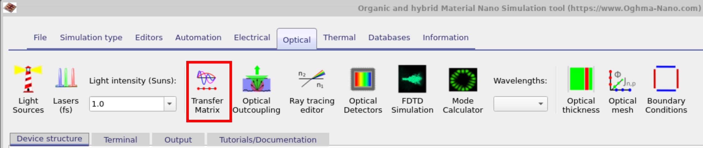
The Transfer Matrix simulation tool can be accessed from the Optical ribbon in the main window by selecting Transfer matrix (see Figure ??).
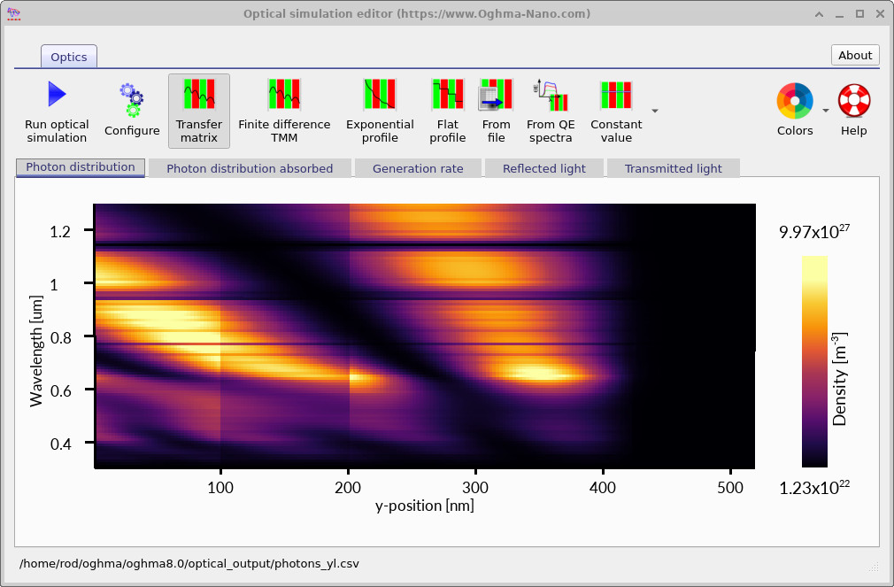
Clicking Run optical simulation (see Figure ??) calculates the optical field distribution within the device and derives quantities such as the photon density, absorbed photon density, generation rate, reflection spectrum, and transmission spectrum. The optical simulation window also provides access to alternative optical models including the transfer matrix method, finite-difference TMM, exponential generation profiles, and user-defined generation profiles.
3. Simulation Modes
Although this window is primarily associated with the transfer matrix simulation, several optical models are available. Some perform a full transfer matrix calculation, while others implement simplifications or variations of the method that can be useful for understanding device behaviour, testing assumptions, or reducing simulation complexity.
- Transfer matrix: Performs a classical transfer matrix calculation using the multilayer formalism described in Transfer Matrix Theory. In this approach the device is represented as a stack of layers and the optical field is propagated through the structure using transfer matrices. Multiple reflections, interference effects, transmission losses, and optical absorption are all included. This is the recommended optical model for conventional layered devices such as solar cells, OLEDs, optical filters, and thin-film sensors.
- Finite difference TMM: Performs the same optical calculation using a finite-difference representation of the optical wave equation. Rather than propagating matrices from layer to layer, the device is divided into a mesh and the forward- and backward-propagating optical fields are solved between neighbouring mesh points. For conventional layered structures the results are usually almost identical to those obtained using the classical transfer matrix method, with any differences typically arising from numerical discretisation. The advantage of the finite-difference approach is that some devices do not naturally lend themselves to a simple layer-based description. Examples include three-dimensional perovskite modules, graded structures, or DFB gratings, where the geometry may still contain layers but is more naturally described using a finite-difference mesh. In these situations the finite-difference formulation often integrates more naturally with the rest of the simulation workflow. Further details are given in Transfer Matrix Theory - Solving in One Large Matrix.
- Exponential profile: Approximates light absorption using an exponential decay: \[I = I_{0} e^{-\alpha x}\] Transmission between layers is given by: \[T = 1 - \frac{n_1 - n_0}{n_1 + n_0}\] Reflections and interference effects are neglected. This model is often useful when trying to understand the operation of a device because it removes cavity effects and standing waves from the problem, allowing the influence of optical absorption to be examined in isolation.
- Flat profile: Calculates transmission losses at interfaces using \[T = 1 - \frac{n_1 - n_0}{n_1 + n_0}\] and then converts the resulting generation profile into a spatially uniform profile within each layer. This approximation is useful when studying carrier transport, trapping, recombination, or dynamic electrical behaviour, where a strongly position-dependent generation profile can obscure the underlying physics. By removing spatial variation in the optical generation rate it is often easier to understand how the electrical model behaves.
- From file: Imports a generation profile from an external file rather than calculating it internally. Generation profiles may be imported from external optical simulations or generated from quantum-efficiency spectra.
- Constant value: Allows a fixed generation rate to be specified directly within each layer. This mode is useful for simplified studies, fitting exercises, and parameter sweeps where the detailed optical behaviour is not important. For example, it can be used to investigate how quantities such as the short-circuit current or open-circuit voltage vary as a function of generation rate.
For most simulations either the classical Transfer Matrix solver or the Finite Difference TMM solver should be used. The remaining modes are simplified approximations intended to provide additional physical insight, support fitting and debugging, or allow externally generated optical profiles to be incorporated into the simulation.
4. Output files
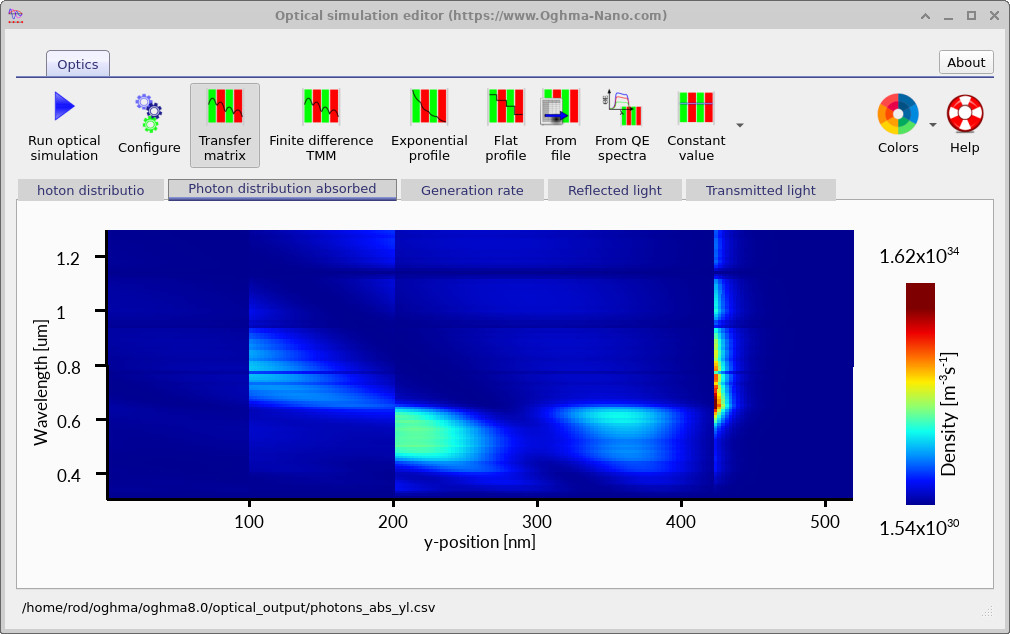
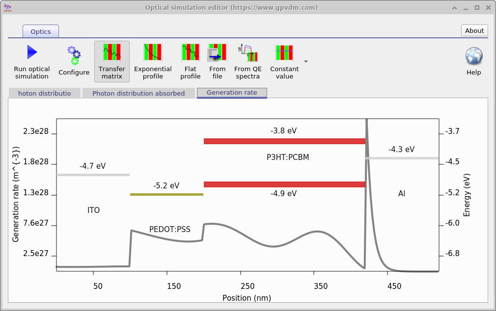
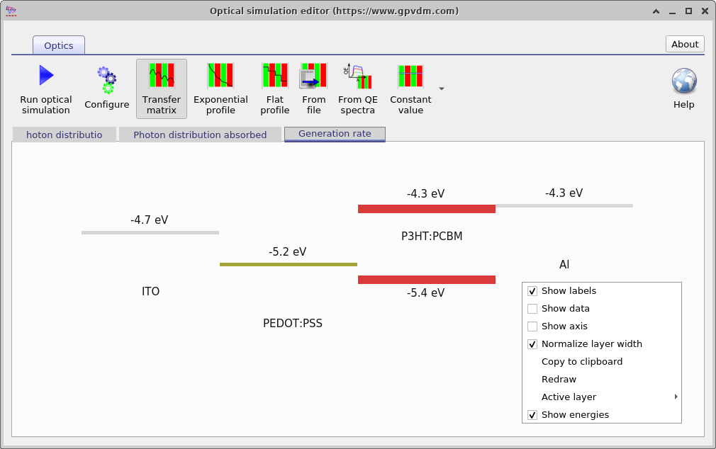
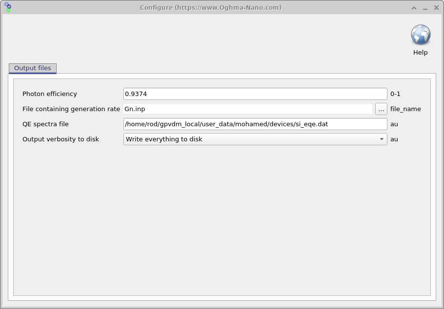
The optical simulation window provides several tabs that allow you to explore how light interacts with the device. For example, ?? shows the photon density inside the structure, where reflections at the layer interfaces give rise to clear interference patterns. ?? presents the same data as ??, but displayed as a band diagram. This alternative view is accessed by right-clicking in the window and adjusting the menu options, and is particularly useful for generating band diagram figures for publications. Finally, ?? shows the configuration window of the optical model. A key parameter here is the photon efficiency, which specifies how many electron–hole pairs are created per absorbed photon. In organic devices, this parameter accounts for geminate recombination, whereas in inorganic or well-ordered systems it should typically be set close to 1.0.
Overview: After running an optical simulation, an overview of the results can be viewed in the optical simulation window (??), as described above. For more detailed analysis, additional information is available in the Output tab of the main window (??). In ?? two key icons are visible: optical_output and optical_snapshots. Double-clicking optical_output opens the optical results window (Figure ??), while double-clicking optical_snapshots opens the Optical Snapshots window (??). The Optical Snapshots window allows you to inspect wavelength-resolved data such as photon density, absorbed photons, and electric field distributions within the device. Because results are stored for each wavelength, this tool provides a detailed view of device performance across the optical spectrum.
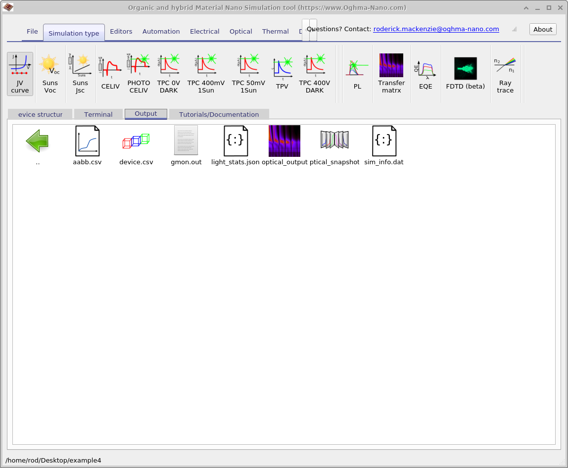
optical_output and optical_snapshots are usually only generated when the optical simulation is run directly,
and are not written when the optical solver is called as part of a coupled electrical simulation.
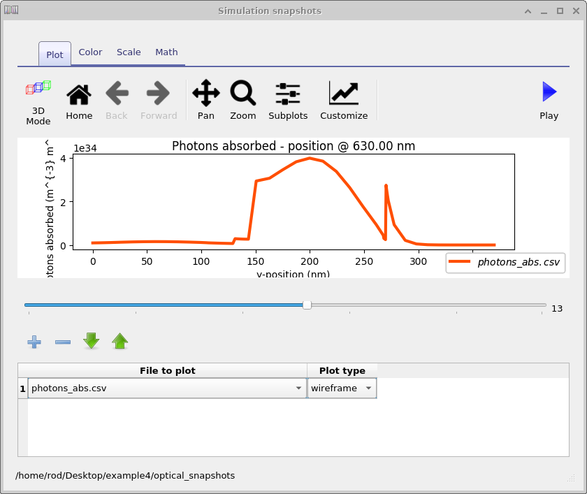
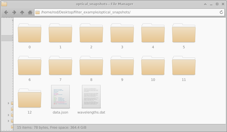
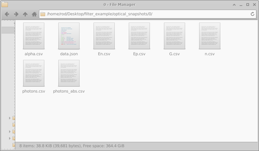
Optical_snapshots: The optical_snapshots folder described above provides access to photon density, absorbed photons, and the optical electric field as a function of wavelength when viewed through the graphical interface. However, it is simply a standard directory and can also be explored directly in a file manager. As shown in Figure ??, the folder contains subdirectories numbered from 0 to 12, each corresponding to a single simulated wavelength. Opening one of these subdirectories (for example, directory 0) reveals the output files shown in Figure ??.
These files include data such as absorption profiles, electric fields, photon densities, and generation rates, all written in plain-text CSV format for easy inspection or post-processing. The table below summarises the contents of a typical wavelength directory:
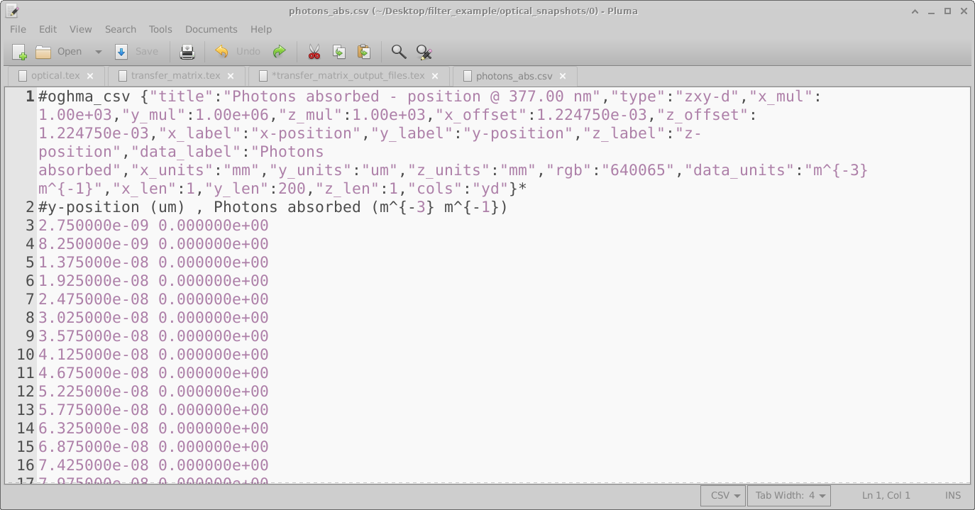
photons_abs.csv, showing metadata followed by axis labels and data values.
Since these outputs are plain text, they can be opened with any editor. As shown in Figure ??, the first line of each CSV contains metadata for plotting, the second line describes the axes, and the remaining lines provide the raw numerical data.
| File name | Description |
|---|---|
alpha.csv |
y-position vs. absorption at the selected wavelength |
data.json |
JSON metadata file including wavelength value and plotting information |
En.csv |
y-position (m) vs. electric field, negative component (V/m) |
Ep.csv |
y-position (m) vs. electric field, positive component (V/m) |
G.csv |
y-position (m) vs. generation rate (\(m^{-3}s^{-1}\)) |
n.csv |
y-position (m) vs. real part of the refractive index n |
photons.csv |
y-position (m) vs. photon density (\(m^{-3}\)) |
photons_abs.csv |
y-position (m) vs. absorbed photons (\(m^{-3}s^{-1}\)) |
The optical_output folder in depth:
While the optical_snapshots directory stores wavelength-resolved results (one subfolder per simulated wavelength),
the optical_output directory contains wavelength-integrated data in the form of two-dimensional maps of
wavelength vs. position.
These outputs provide an overview of how light interacts with the device across the full spectrum, including key
quantities such as charge-carrier generation rate, photon density, normalized photon density, transmission, and reflection.
The contents of the directory are shown in
Figure ??.
The files listed in Figure ?? are described in detail in Table ??.
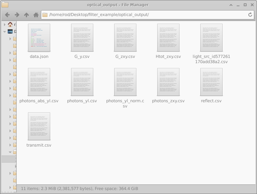
optical_output directory, containing wavelength-integrated summary files generated by the Transfer Matrix solver.
| File name | Description | Plot type |
|---|---|---|
data.json |
Metadata file with simulation settings in JSON format | 1D |
G_y.csv |
y-position (m) vs. charge generation rate (\(m^{-3} s^{-1}\)) | 2D |
G_zxy.csv |
zxy-position (m) vs. charge generation rate (\(m^{-3} s^{-1}\)) | 2D |
Htot_zxy.csv |
zxy-position (m) vs. optical heat generation (\(W m^{-3}\)) | 2D |
light_src_id_xxx.csv |
Wavelength (m) vs. light intensity from a specified source (\(W/m\)) | 2D |
photons_abs_yl.csv |
Wavelength (m) vs. y-position (m) vs. absorbed photons (\(m^{-3} s^{-1}\)) | 2D |
photons_yl.csv |
Wavelength (m) vs. y-position (m) vs. photon density (\(m^{-3}\)) | 2D |
photons_yl_norm.csv |
Wavelength (m) vs. y-position (m) vs. normalized photon density (a.u.) | 2D |
reflect.csv |
Wavelength (m) vs. reflected light from the device stack | 1D |
transmit.csv |
Wavelength (m) vs. transmitted light through the device stack | 1D |
6. Simulating optically thick layers (incoherent layers)
Typical optoelectronic devices have active layers between 10 nm and 100 nm thick. However, these devices are often deposited on substrates that are 10 mm to 1 cm thick. In many cases it is useful to simulate not only the device itself but also the optical effects of the substrate. This requires a simulation tool that can span length scales from nanometres up to metres. There are three main challenges with doing this:
- Problem 1: Simulating different length scales – Numerical solvers struggle when handling very large and very small numbers in the same calculation. This can lead to rounding and numerical errors.
- Problem 2: Wavelength of light – Because the wavelength of visible light is much smaller than 1 cm, simulating a centimetre-thick layer requires an impractically fine spatial mesh to capture interference effects.
- Problem 3: Loss of coherence – The transfer matrix model assumes light enters at normal incidence and that layers are defect-free. In thick substrates, scattering and inhomogeneities break these assumptions, and the light field becomes incoherent.
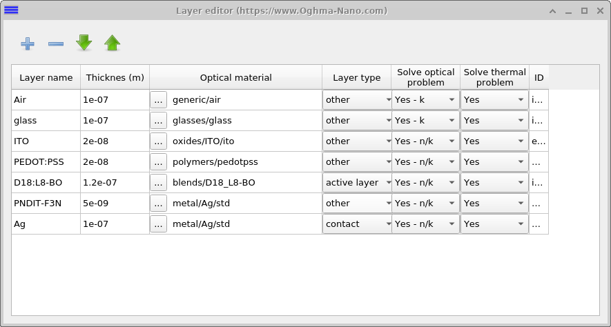
OghmaNano addresses these issues in two ways. First, it allows the user to treat a layer as incoherent, considering only absorption and neglecting phase information. This approach resolves Problems 2 and 3. The option can be set in the layer editor (Figure ??). In the column labelled Solve optical problem, layers marked Yes – n/k include both phase and absorption, while those marked Yes – k account only for attenuation, effectively treating them as incoherent layers.
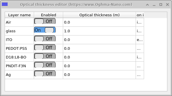
Second, to handle Problem 1 (large differences in length scale), OghmaNano allows an effective optical thickness to be assigned to any layer. For example, a substrate might be defined as 100 nm thick in the layer editor but assigned an effective depth of 1 m. Internally, this is implemented by scaling the absorption coefficient:
\[\alpha_{\text{effective}}(\lambda) = \alpha(\lambda)\,\frac{L_{\text{effective}}}{L_{\text{simulation}}}\]
where \(\alpha_{\text{effective}}\) is the scaled absorption used in the simulation, \(\alpha\) is the material absorption coefficient, \(L_{\text{effective}}\) is the desired effective thickness (e.g. 1 m), and \(L_{\text{simulation}}\) is the actual layer thickness in the editor. This approach reduces numerical issues and also produces more useful plots, where the substrate does not dominate the axes and the device layers remain clearly visible.
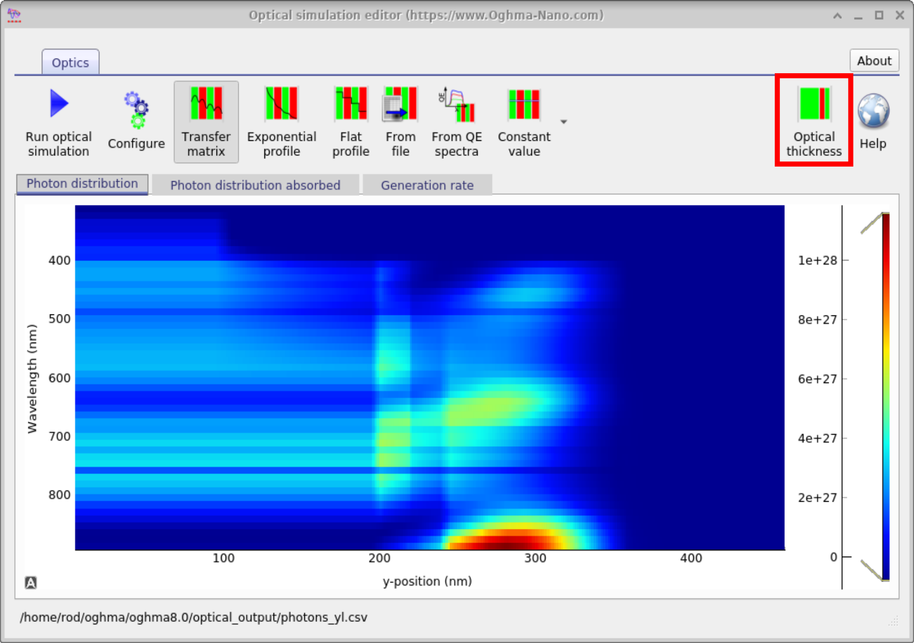
To use this feature, set up the device structure as shown in Figure ??. Then, in the Transfer Matrix window, click the Optical Thickness button (Figure ??). This opens the configuration dialog (Figure ??), where the effective optical thickness of any layer can be specified. In the example shown, the glass substrate is set to 1 m.
4. When is the TMM run?
The transfer matrix simulation can be run in two ways. First, it can be launched directly by clicking the Play button. Alternatively, the optical model is executed automatically whenever an electrical simulation is run, requiring no additional user action.
The main difference between these two modes is in the output. When run directly, the optical simulation generates a more complete set of output files on disk. In contrast, when it is invoked as part of an electrical simulation, the output is reduced to essential data only, in order to avoid slowing down the electrical solver.
👉 TMM theory: Go to the next section to understand transfer matrix theory.