Exciton Domain Tutorial (Part B): Editing Geometry and Optical Properties
1. Editing the shape of the domain
In real bulk heterojunction systems, donor domains are neither perfectly spherical nor uniform. Their size, shape, and connectivity vary on the nanometre scale, and these geometric features directly influence how far excitons must diffuse before reaching a donor–acceptor interface. Because the exciton-domain model is fully three-dimensional and mesh-based, it allows you to explore how changes in domain morphology—beyond simple size variations—affect exciton transport and dissociation.
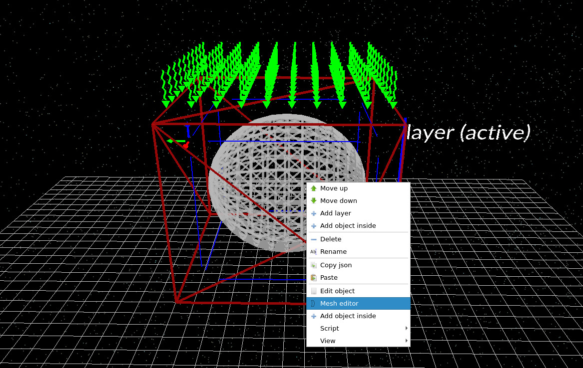
To modify the domain geometry, right-click on the embedded object (the sphere in the default example) in the main simulation window. The context menu is shown in Figure ??. Select Mesh editor to open the geometry editor.
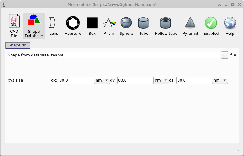
Within the mesh editor, you can choose from a library of predefined shapes or import your own geometries. The exciton solver is agnostic to topology: as long as the shape can be meshed, it can be used as a donor domain. For illustration, we will replace the sphere with a teapot-shaped domain, scaled to nanometre dimensions. Although clearly not a realistic morphology for a BHJ, this deliberately complex, nanoscale shape provides an intuitive way to see how curvature, concavity, and local thickness influence exciton diffusion paths and interfacial dissociation.
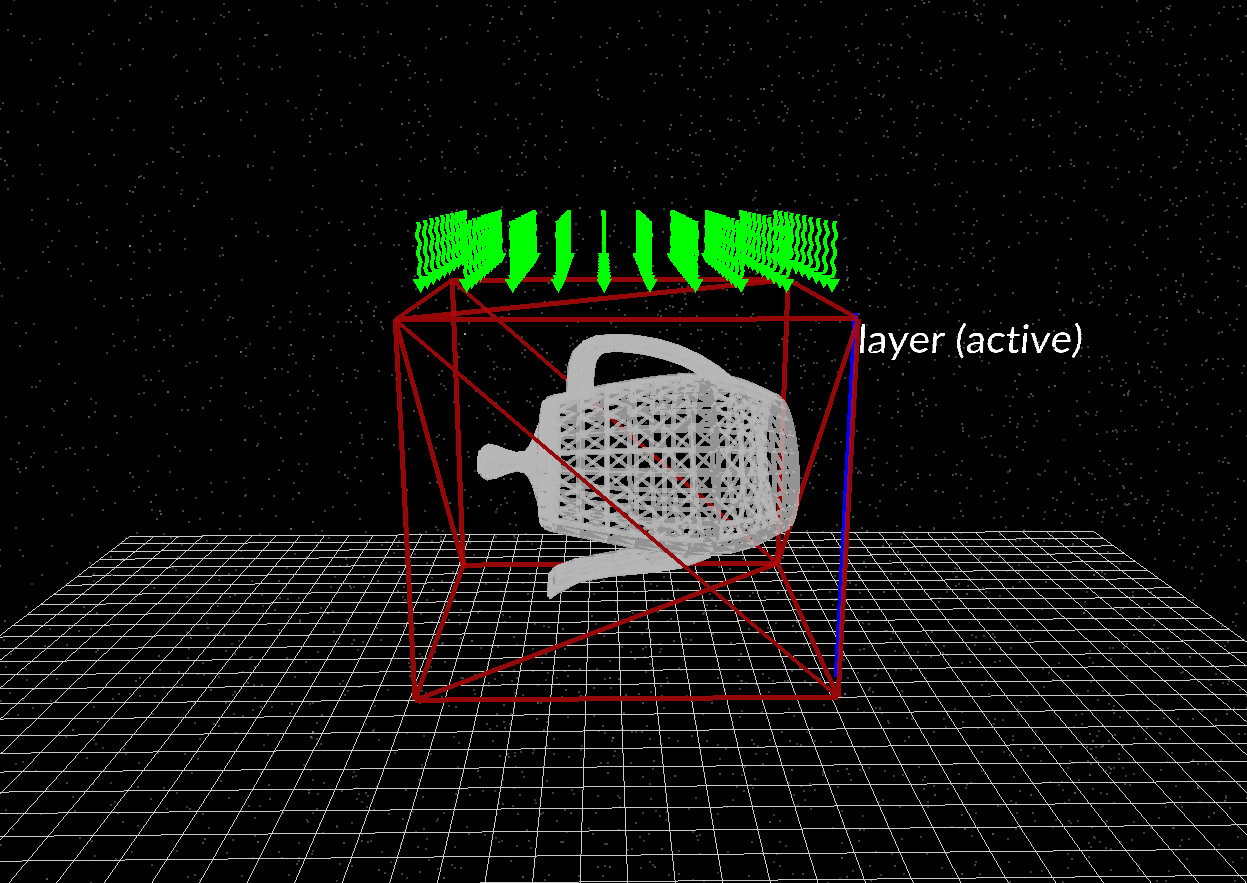
Select the teapot shape by clicking the shape database selector (the three dots button), then double-click teapot. Close the mesh editor. The main simulation window updates automatically, as shown in Figure ??.
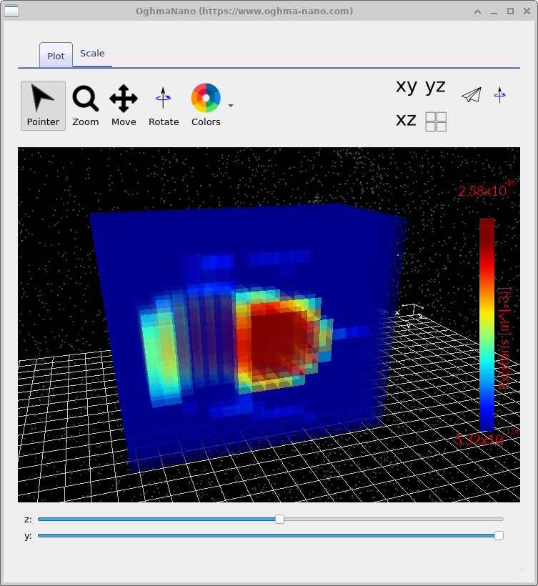
Run the simulation as before. Once it completes, navigate to Exciton Output and open
exciton.csv. The resulting exciton density field is shown in
Figure ??. Although the specific shape used here is artificial, the underlying physics is identical to the spherical case: excitons are generated within the donor, diffuse through the three-dimensional domain, and are removed at interfaces where dissociation is strong. The value of this approach is that the geometry can be replaced with any shape of interest, making the model well suited for
systematic what-if studies of how domain morphology influences exciton transport and
effective charge generation.
2. Optical properties
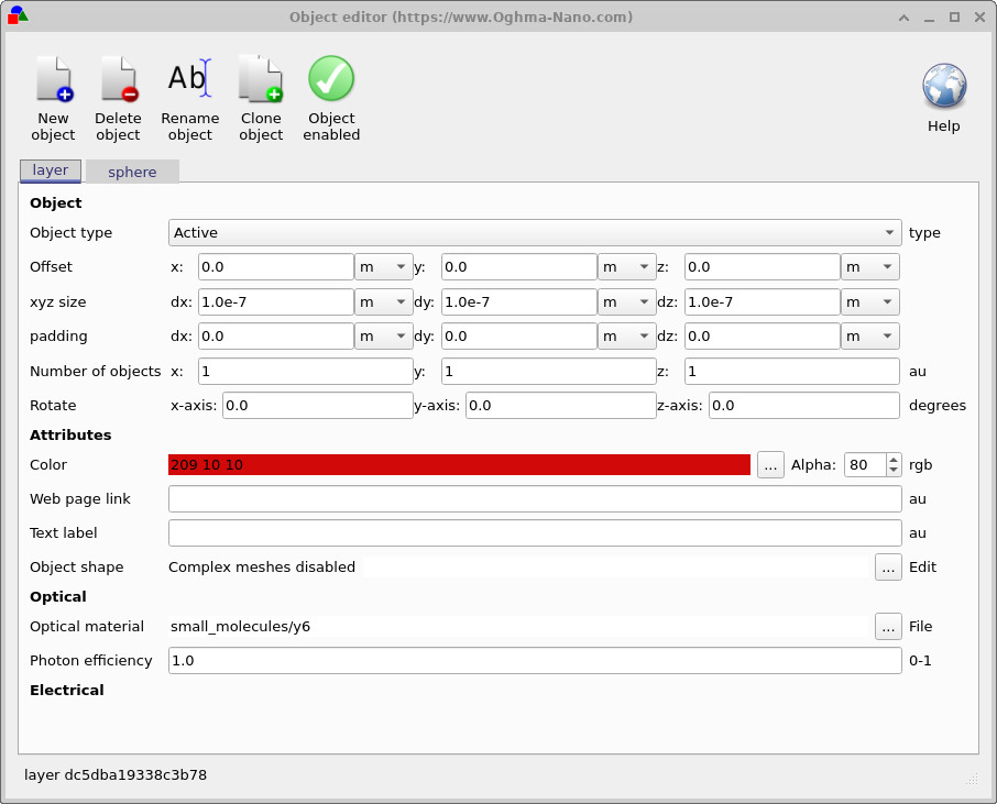
Optical properties in the exciton-domain model are assigned on a per-object basis. To edit them, right-click on either the surrounding layer or the embedded donor domain and select Object editor. This opens the object editor window shown in Figure ??. Each object can be associated with a specific optical material, and these materials include wavelength-dependent refractive index data (\(n,k\)). In a full optical simulation, these material properties would be used to determine how light is absorbed spatially within the structure and how excitons are generated as a function of position and wavelength.
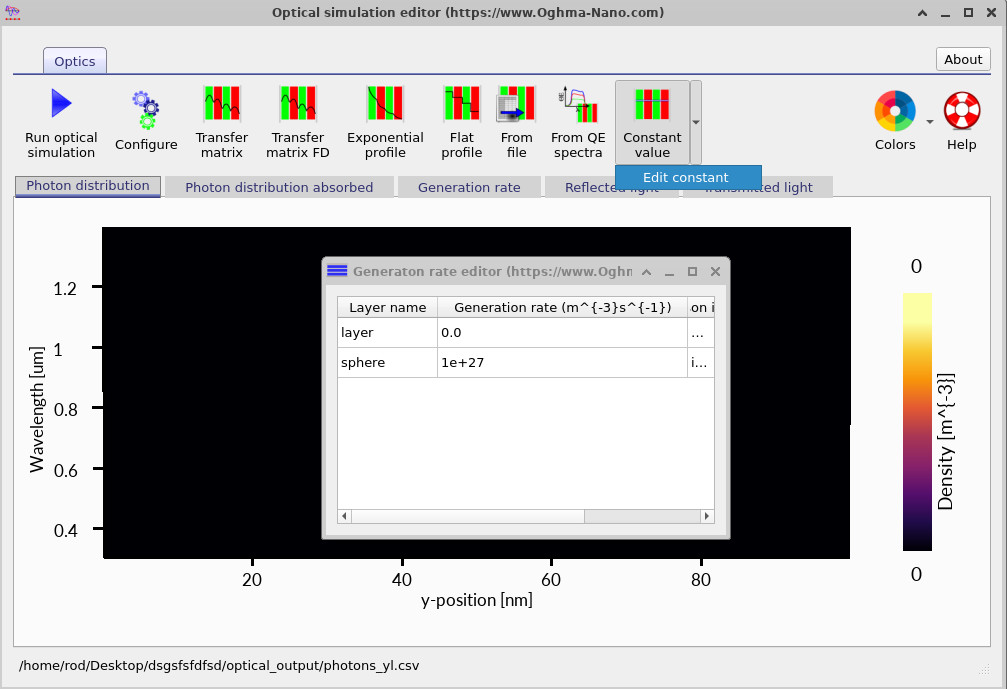
In this tutorial, the optical material data (the assigned \(n,k\) for each object) are deliberately not used to compute absorption. Instead, exciton generation is prescribed directly using a constant exciton generation rate. This is a conscious modelling choice designed to isolate exciton transport, recombination, and interfacial dissociation from optical interference and wavelength-dependent effects. The corresponding configuration is set in the optical simulation editor, accessed from the Optical ribbon in the main window, and is shown in Figure ??.
In the optical editor, the generation model is currently set to Constant value. The object-wise generation rates can be viewed by opening the drop-down menu associated with Constant value and selecting Edit constant. This opens the generation-rate editor shown inset in the figure, which lists the prescribed generation rate for each object in the scene. In the present configuration, the donor domain (sphere or teapot) is assigned a uniform generation rate of \(1\times10^{27}\,\mathrm{m^{-3}\,s^{-1}}\), while the surrounding layer is assigned zero. This produces a spatially uniform exciton source confined to the donor region. Because the generation rate is fixed and known everywhere, the resulting exciton density and dissociation patterns can be interpreted directly in terms of diffusion, recombination, and interfacial loss processes, without the additional ambiguity introduced by wavelength-dependent absorption profiles.
💡 Why this matters: With a fixed generation rate, every exciton entering the system is accounted for. This makes it much easier to understand where excitons are lost, where they dissociate, and how changes in diffusion length, lifetime, or interface strength alter the overall charge-generation yield.
With the geometry and optical generation defined, the exciton-domain model is now complete.
You can proceed to explore how changes in domain shape, size, and exciton parameters affect
the dissociation efficiency reported in exciton_sim_info.json.
👉 End of tutorial: You have completed the 3D exciton-domain tutorial. The same modelling workflow can be applied to arbitrary three-dimensional meshes, imported morphologies, or experimentally reconstructed donor–acceptor domains. This makes the exciton-domain solver a practical tool for studying how nanoscale morphology, diffusion length, lifetime, and interfacial dissociation collectively control exciton transport and charge-generation efficiency in organic and hybrid semiconductor systems.
📘 Return to the introduction to organic electronics for a broader overview of the topic.