2D slab waveguide mode solver (TE/TM)
In this tutorial we calculate the guided optical modes supported by 2D slab waveguide structures using the OghmaNano optical mode solver. The tutorial demonstrates how to construct optical meshes, solve transverse electric (TE) and transverse magnetic (TM) eigenmodes, and visualise confined optical field distributions in dielectric waveguides.
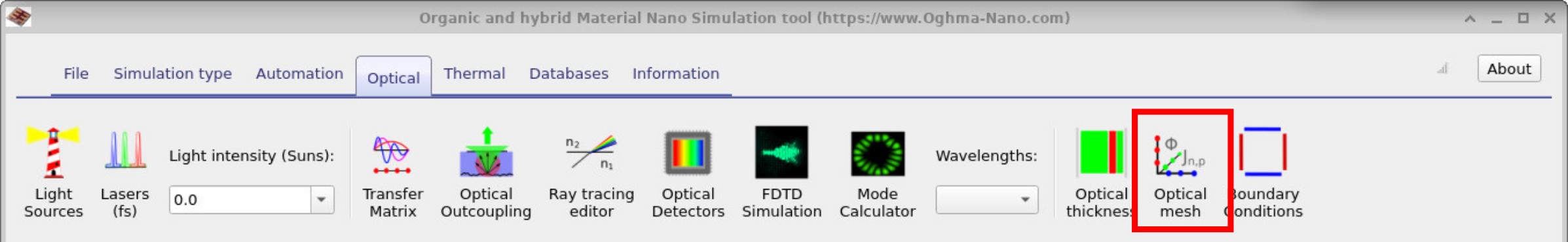
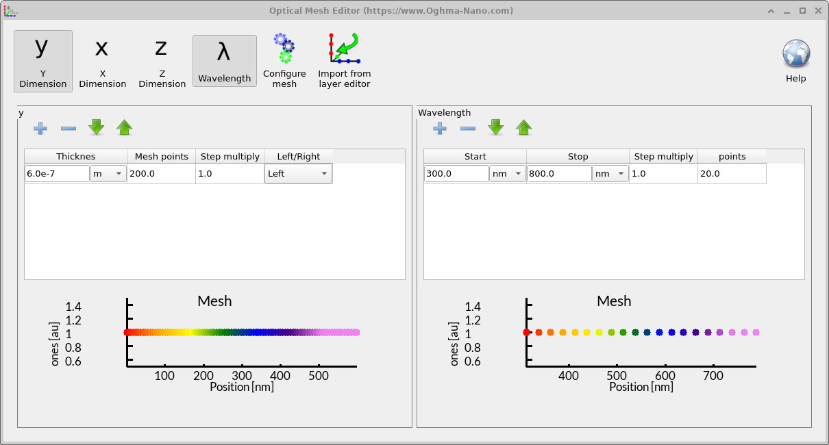
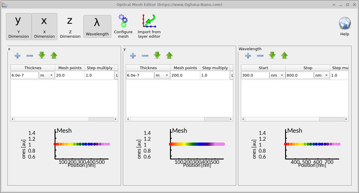
1. Constructing a 2D slab waveguide
Open New simulation → Mode solvers and select the 1D slab waveguide example. Configure the layer stack (e.g., 500 nm / 500 nm / 500 nm) and refractive indices (n = 1 / 4 / 1 for cladding / core / cladding in this example). Set polarization to Transverse electric (TE).
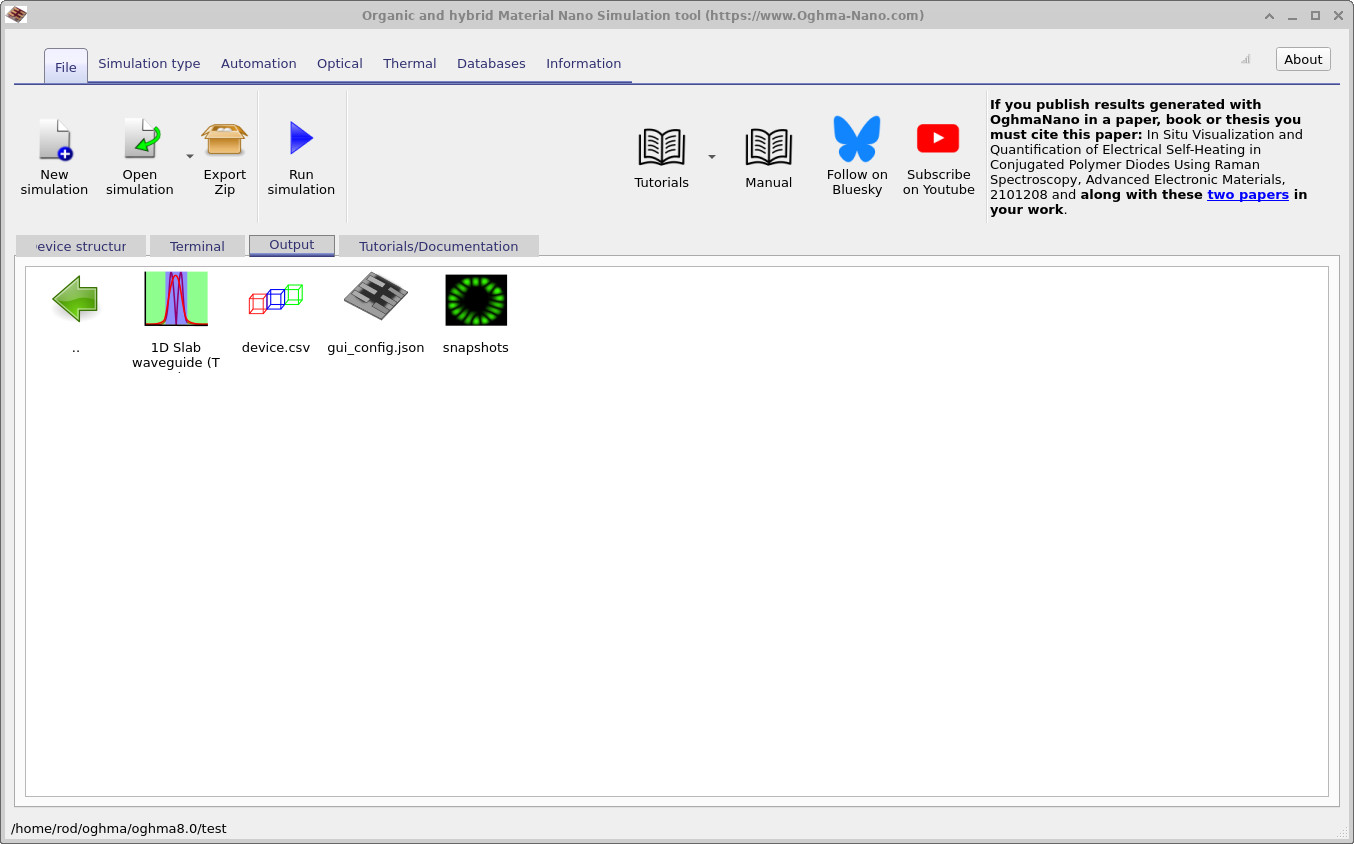
👉 Next step: Now continue to Part C for a more detailed OPV tutorial, including outputs, device layers, and advanced analysis.