Part A: OLED device simulation - coherent thin-film optics
1. Overview of simulating OLEDs

Organic Light Emitting Diodes (OLEDs) are widely used in modern display and lighting technologies, and their performance is strongly determined by the coupled electrical and optical processes inside the device. In an OLED, charge carriers are injected from the electrodes into organic thin films, where radiative recombination produces light via electroluminescence. In OghmaNano, OLED device simulation is performed by combining drift–diffusion charge-transport modelling with optical models, allowing both current flow and light generation to be treated self-consistently.
In this tutorial, we present a step-by-step OLED device simulation in OghmaNano using a single-emissive-layer (single-EML) structure. The electrical behaviour is solved self-consistently using the drift–diffusion equations, while the optical response is modelled using the transfer matrix method (TMM). The transfer matrix method treats light as a coherent wave and provides a rigorous thin-film optical description of propagation, reflection, and interference within the layered OLED stack.
This coherent optical model is particularly well suited to smooth, planar OLED structures such as evaporated thin films, where microcavity effects and thin-film interference play a central role. When coupled to the electrical simulation, the model enables direct calculation of current–voltage characteristics, voltage-dependent external quantum efficiency (EQE), emission spectra, and colour-related quantities, capturing the essential physics of electro–optical coupling in OLEDs.
2. Making a new simulation
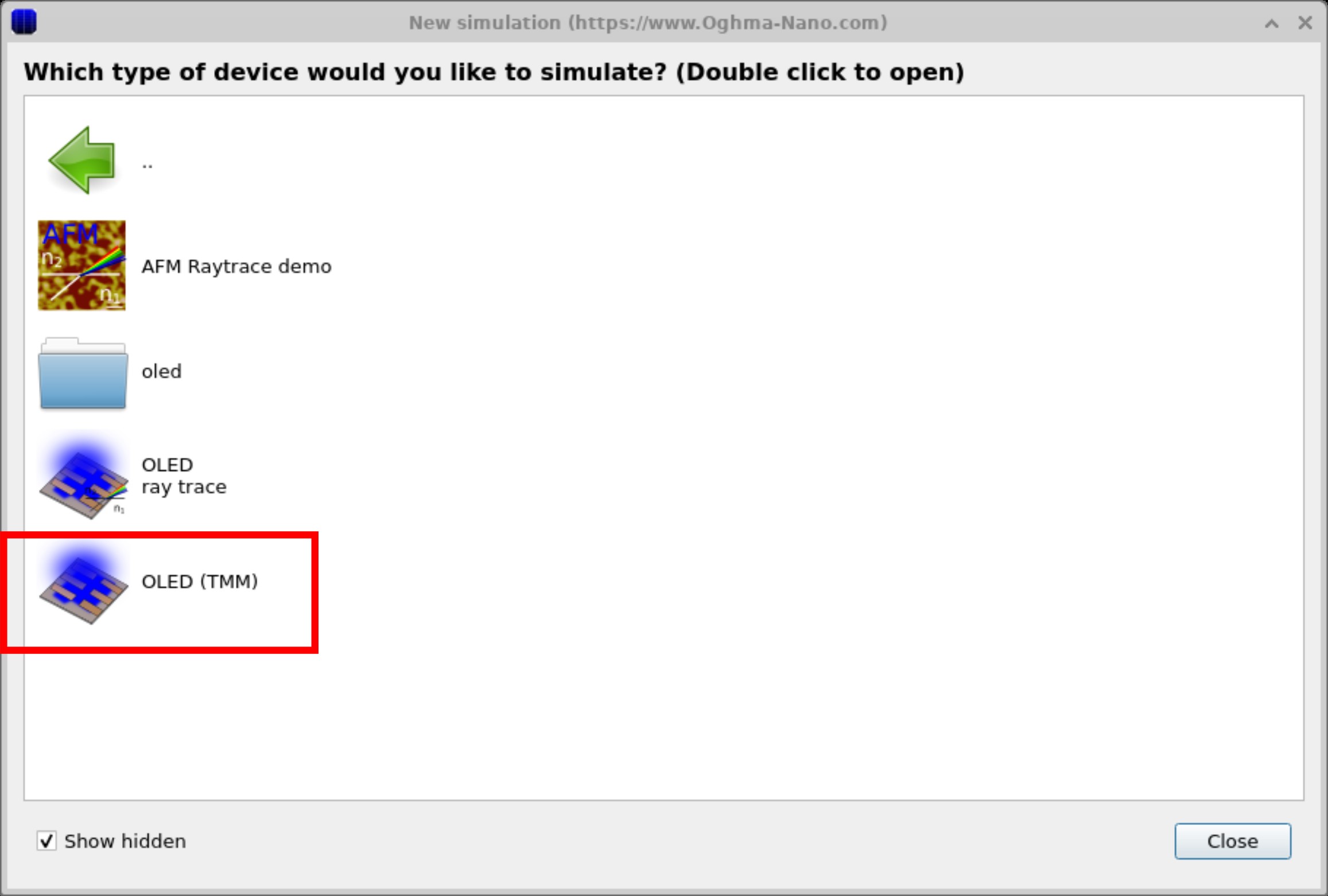
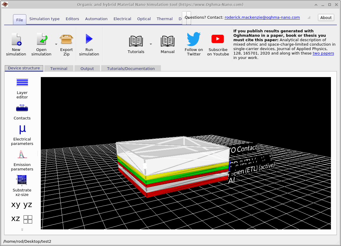
To begin, open the OLED (TMM) example simulation by double-clicking it in the New simulation window. This loads the main interface shown in ??, where the device stack and associated editor panels are displayed.
3. Exploring optical-only simulations

A key challenge in OLED design is determining how much of the light generated inside the device ultimately escapes into free space. A large fraction of photons remain trapped within the layered structure or are absorbed before they can contribute to useful emission. The transfer matrix method (TMM) provides a quantitative framework for analysing how interference within the thin-film stack redistributes optical power, and how changes in layer thickness or refractive index influence the fraction of light that is extracted.
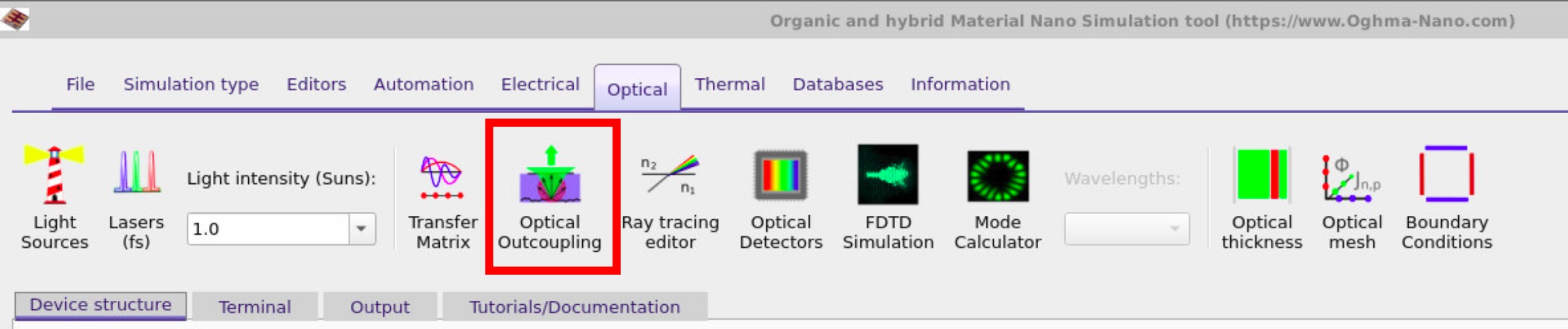
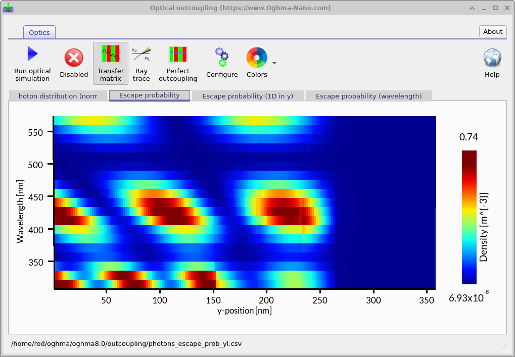
To access the optical tools, switch to the Optical ribbon (??) and click on the Optical outcoupling button. This opens the Optical outcoupling tool, shown in ??, where transfer-matrix calculations can be run independently of the electrical solver.
To begin the calculation, click the Play button. The simulation computes the spatial and spectral distribution of emitted photons within the OLED stack. The resulting plot, ??, shows the escape probability as a function of wavelength (vertical axis) and position within the device (horizontal axis). Bright regions indicate combinations of emission wavelength and depth where photons have a high probability of escaping to the outside world, while darker regions correspond to light that remains trapped within the structure.
The alternating bands visible in this plot arise from constructive and destructive interference between forward- and backward-propagating optical waves within the OLED microcavity. This behaviour is directly analogous to the standing-wave patterns observed in a ripple tank (??), where reflections at the boundaries cause water waves to interfere, producing regions of enhanced and suppressed wave amplitude. In the OLED, the same wave physics governs how optical energy is redistributed across the stack, giving rise to the characteristic interference pattern seen in the escape-probability map.
Such optical-only simulations provide direct insight into how the layered microcavity shapes emission and offer practical guidance for optimising layer thicknesses and emission wavelengths prior to full coupled electrical–optical modelling.
3. Electrical simulations combined with optical transfer matrix calculations
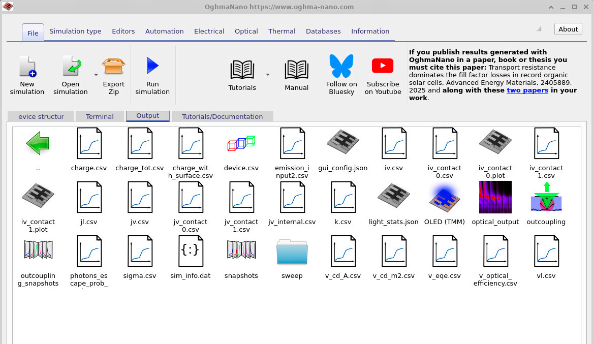
Now that you have explored optical outcoupling with the Transfer Matrix Method (TMM), you can combine this with drift–diffusion modeling to understand how an OLED emits light as a function of current and voltage. In these combined simulations, the recombination profile from the drift–diffusion calculation provides the emissive source, which is then coupled into the optical outcoupling model. The simulation first performs an optical outcoupling calculation, just as described above, and then runs a standard electrical drift–diffusion simulation to generate the current–voltage (JV) response. The user should return to the main interface and press the Run simulation button (▶) to launch the full calculation. The results of the combined electro–optical simulation are written to the Output tab and appear as shown in ??.
| File name | Description |
|---|---|
iv.csv |
Current vs. voltage |
jv.csv |
Current density vs. voltage |
jl.csv |
Current density vs. optical output power density |
k.csv |
Averaged recombination rate constant vs. voltage |
v_eqe.csv |
Voltage vs. external quantum efficiency (EQE) |
vl.csv |
Voltage vs. optical output power density |
v_cd_a.csv |
Luminance efficiency (cd A−1) vs. voltage |
v_cd_m2.csv |
Luminance (cd m−2) vs. voltage |
sweep/ |
Values i.e. (mobility, CIE X/Y/Z, carrier density v.s. voltage) |
Snapshots/ |
Snapshots of the electrical device parameters saved at each simulation step. |
The simulation writes a number of output files to the Output tab. These files contain the key numerical results of the combined optical and electrical OLED simulation and can be used for further analysis or plotting. The most important files are described below in Table 7.1.
The key output characteristics of the coupled electrical–optical OLED simulation are shown in
??,
?? and
??.
The current density–voltage curve (jv.csv) shows the electrical turn-on behaviour of the device.
The voltage–luminance curve (v_cd_m2.csv) converts the simulated optical output into display-relevant
units (cd m−2), illustrating how brightness rises rapidly once efficient recombination is established.
Finally, the voltage–EQE curve (v_eqe.csv) shows the onset of light generation at turn-on and, in this
example, a near-constant efficiency once the device is operating in its radiative regime.
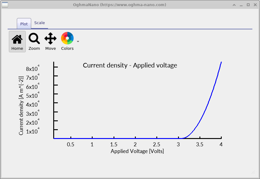
jv.csv) curve from the OLED simulation.
This shows the electrical turn-on and the rapid increase in current with applied voltage.
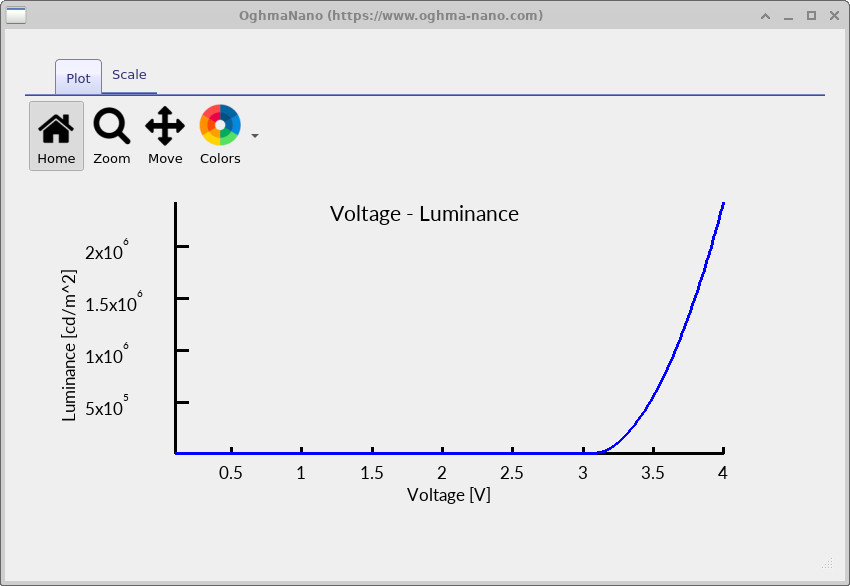
v_cd_m2.csv) curve from the OLED simulation.
Luminance (cd m−2) increases sharply after turn-on as radiative recombination becomes efficient.
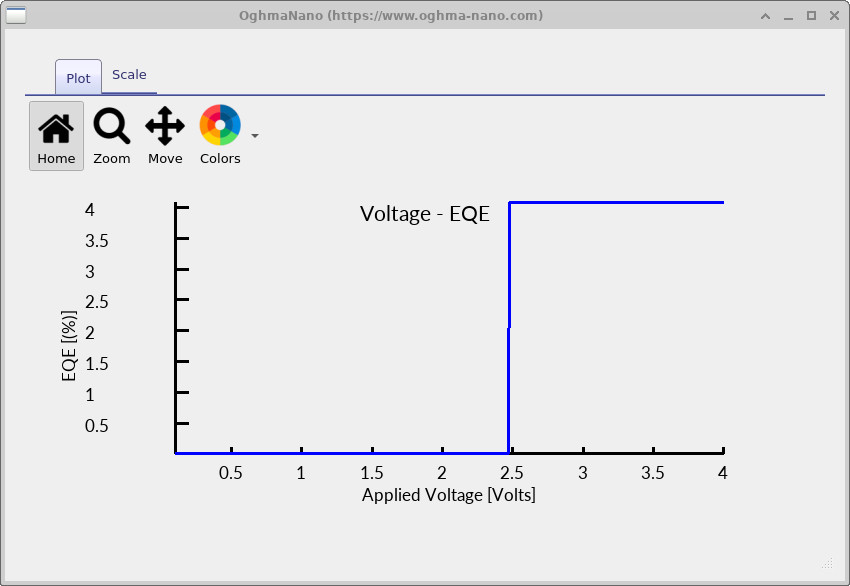
v_eqe.csv) curve from the OLED simulation.
The EQE rises at the turn-on voltage and then remains approximately constant in this example.
4. How is light generated in the device
In an OLED, light is generated through radiative recombination of free electrons and holes within the emissive layer. Electrons injected from the cathode and holes injected from the anode are transported through the device until their spatial distributions overlap, at which point recombination can occur and a photon may be emitted.
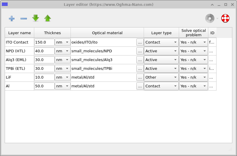
The layer structure of the device is defined in the Layer editor, shown in ??. Layers that participate in charge transport and recombination are explicitly marked as electrically active in this editor, while contacts and optically passive layers are excluded from the electrical solve. In the present device, only the central Alq3 layer is configured as emissive, ensuring that radiative recombination is confined to this region.
The local radiative recombination rate is proportional to the product of the free carrier densities and is written as
\( R = k \left( n p - n_{\mathrm{eq}} p_{\mathrm{eq}} \right) \)
Here, \(n\) and \(p\) denote the free electron and hole densities, respectively, and \(k\) is the radiative recombination coefficient. This expression ensures that recombination vanishes at equilibrium and increases as carrier injection drives the system out of equilibrium under applied bias.
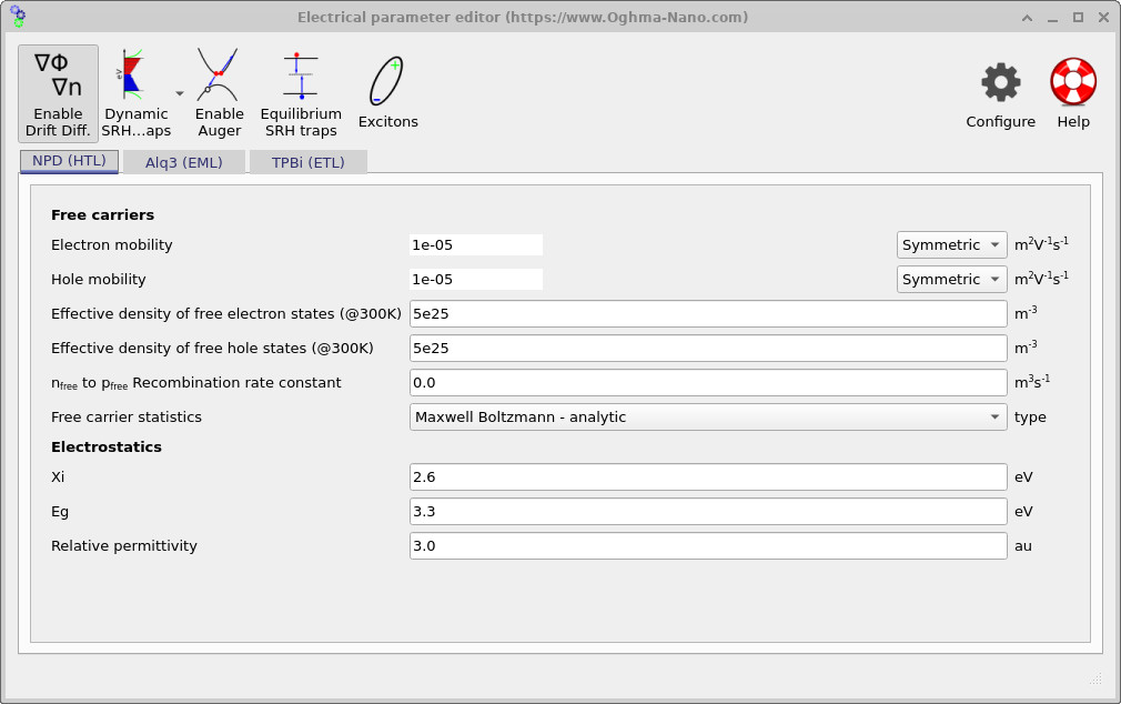
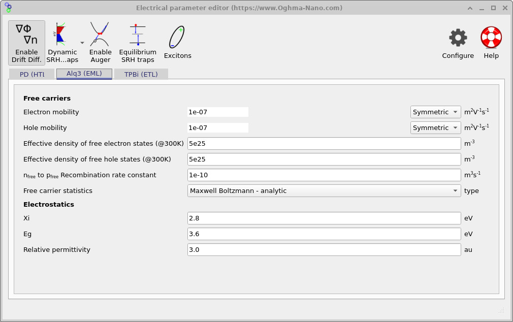
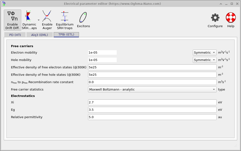
The electrical parameters governing charge transport and recombination are defined in the Electrical parameter editor, which can be accessed from the Device tab in the main window. The parameters used for the present device are shown in ??, ?? and ??, corresponding to the hole-transport layer (HTL), emissive layer (EML), and electron-transport layer (ETL), respectively.
These figures define the carrier mobilities, effective densities of states, electrostatic parameters, and recombination constants used in the drift–diffusion equations. In this example, radiative recombination is enabled only in the emissive Alq3 layer, while the transport layers serve primarily to inject and confine charge carriers. Together, these parameters control where carriers accumulate, where recombination occurs, and ultimately the spatial distribution of light generation within the device.
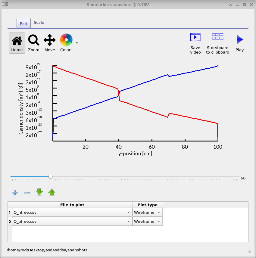
During the simulation, OghmaNano automatically creates a directory named snapshots in the output folder (see ??). The snapshots directory contains electrical and optical quantities recorded at each simulation step, which in this example corresponds to the applied voltage. In addition to device-level outputs, the snapshots include spatially resolved internal solver variables as a function of position within the device, such as quasi-Fermi levels and free carrier densities. Derived quantities and observable outputs, including the external quantum efficiency (EQE), are also recorded, allowing both internal device physics and externally measured quantities to be examined consistently.
Open the snapshots directory to launch the snapshots viewer by double clicking on it. This will open the window shown in ??.
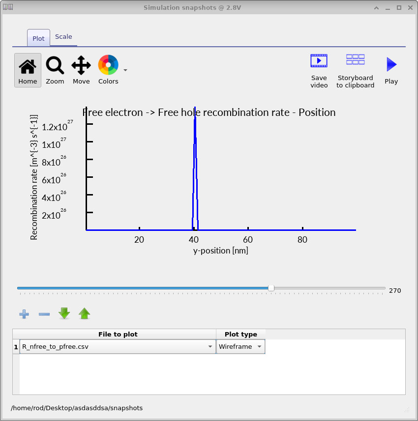
Using the blue + button, add a new plot line and select the relevant file (for example
Q_nfree.csv, Q_pfree.csv, or R_nfree_to_pfree.csv).
As the slider is moved from left to right, the plotted quantity updates for each simulation step, allowing the evolution of
carrier densities and recombination to be inspected as a function of applied voltage.
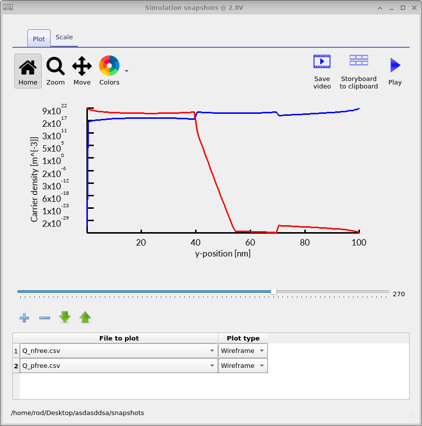
At low applied voltage, the free electron and hole density profiles are shown in ??. As the voltage is increased, the corresponding profiles evolve into those shown in ??. The spatial distributions of electrons and holes are therefore markedly different at low and high bias, which changes where (and how strongly) the carriers overlap in the emission layer.
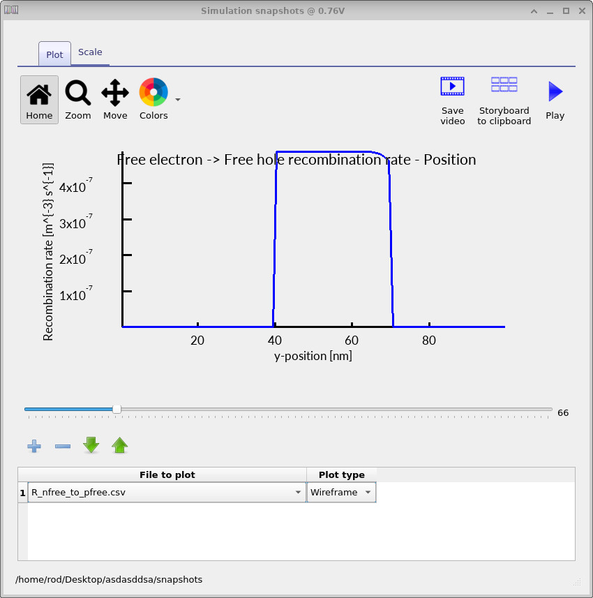
The corresponding free-to-free recombination profiles are shown in the figures ?? (low voltage) and ?? (high voltage). With increasing bias, the recombination zone shifts strongly in position and becomes more localised, indicating that the dominant region of light generation has moved within the device.
5. Translating recombination rate into an emission spectrum
In the previous section, we saw that the free electron and hole densities within the device change significantly as a function of applied voltage. As the applied voltage increases, changes in carrier injection and transport modify the spatial overlap of electrons and holes, causing the recombination rate to increase and the recombination zone to shift within the device. This naturally raises the question of how a spatially varying recombination rate is converted into an emitted optical spectrum within the model.
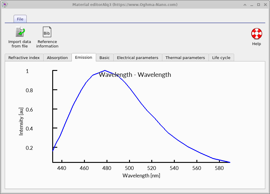
In OghmaNano, one way this is achieved is by using an experimentally measured emission spectrum defined in the materials database . The intrinsic emission spectrum of the emissive material is shown in ??. This spectrum defines the wavelength distribution of photons generated by radiative recombination before optical cavity effects and outcoupling are applied, and has been measured experimental.
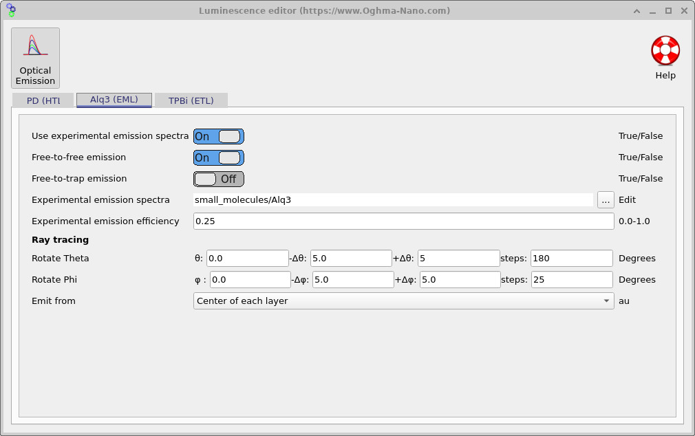
The emission spectrum used by the device is selected in the Luminescence Editor,
shown in ??,
which can be accessed from the Emission parameters in the device structure tab of the main window.
In this example, the emission spectrum is set to
small_molecules/Alq3, corresponding to the experimentally measured emission spectrum
of Alq3.
The three-dot button next to the material path allows the emissive material to be changed.
Also shown in the luminescence editor is the experimental emission efficiency. In the present example this value is set to 0.25, meaning that only 25 percent of electron–hole recombination events result in photon emission. This reflects the spin statistics of electrically generated excitons in fluorescent OLEDs, where only singlet excitons are radiative.
Under electrical excitation, recombination produces singlet and triplet excited states in a 1:3 ratio, so that only one quarter of recombination events populate radiative singlet states, while the remaining triplets are non-radiative. As a result, even in the absence of optical or electrical losses, the internal quantum efficiency is fundamentally limited to 25 percent in this model. This is the primary reason why the EQE and site-resolved EQE in this example device remain relatively low.
In the optical model, the local radiative recombination rate determines how many electron–hole pairs recombine, while the emission efficiency controls what fraction of these events generate photons. The resulting photon generation rate is then distributed over wavelength according to the selected emission spectrum of the material.
\( I(\lambda) = \eta \, R \, S(\lambda) \)
Here, \(R\) is the local radiative recombination rate obtained from the drift–diffusion solver, \(\eta\) is the emission efficiency (set to 0.25 in this example to account for singlet formation), and \(S(\lambda)\) is the normalized emission spectrum stored in the materials database.
More sophisticated OLED models can explicitly treat multiple excited-state populations, including separate singlet and triplet species in the emissive material and a photon rate-equation description of light generation. These models are primarily intended for research use, where detailed excited-state dynamics are of interest, rather than for routine device optimisation. The implementation of these excited-state models in OghmaNano is described in Excited states and emission processes .
6. Examining the luminescence, EQE, and colour as a function of voltage
A characteristic feature of many OLEDs is that the emitted colour changes with applied voltage, even when the emissive material itself is unchanged. As the bias increases, carrier injection alters the spatial overlap of electrons and holes, causing the recombination zone to shift position within the device. Because the OLED stack acts as an optical cavity, different positions within the cavity favour the extraction of different wavelengths. Recombination occurring closer to one interface may preferentially outcouple shorter wavelengths, while recombination elsewhere may favour longer wavelengths. As the recombination zone moves with voltage, the cavity therefore selects different parts of the emission spectrum, leading directly to a voltage-dependent colour shift.
In a well-designed OLED, the emitted colour changes only weakly with applied voltage. This is achieved by keeping the recombination zone confined to a region of the optical cavity where the wavelength-dependent outcoupling varies slowly with position. In practice, this often means designing the emissive region to be relatively thin, so that even if the recombination profile shifts slightly with bias, the cavity selects nearly the same wavelengths.
In this example, we intentionally move away from this optimised regime in order to make the underlying physics more visible. By increasing the thickness of the Alq3 emission layer to 100 nm in the Layer Editor (see ??), we create a larger region over which recombination can occur. This allows pronounced voltage-dependent shifts in the recombination zone to develop, making it easier to observe how changes in carrier injection and transport translate into changes in the optical cavity response.
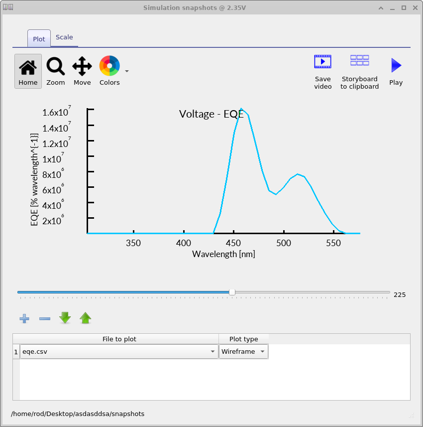
After updating the emission-layer thickness, rerun the simulation. Now use the snapshot tool to plot eqe.csv, add this using the + button.
The plot shows the EQE as a function of wavelength for the currently selected voltage step.
By sweeping the slider through the voltage range, you can observe how the EQE spectrum reshapes as the recombination
zone moves within the cavity and different wavelengths are extracted with different efficiencies.
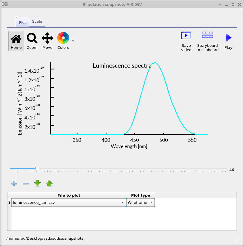
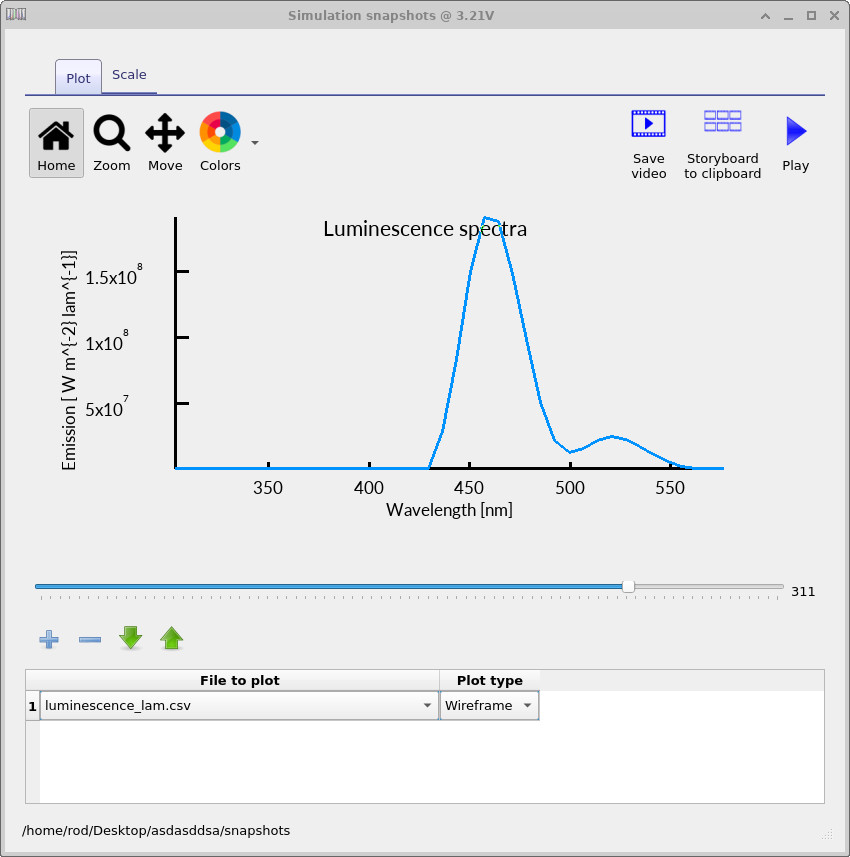
The same workflow can be used to examine the voltage-dependent luminescence spectrum.
Add a plot line for luminescence_lambda.csv and sweep the slider to see how the emission spectrum evolves with
bias (see
?? and
??).
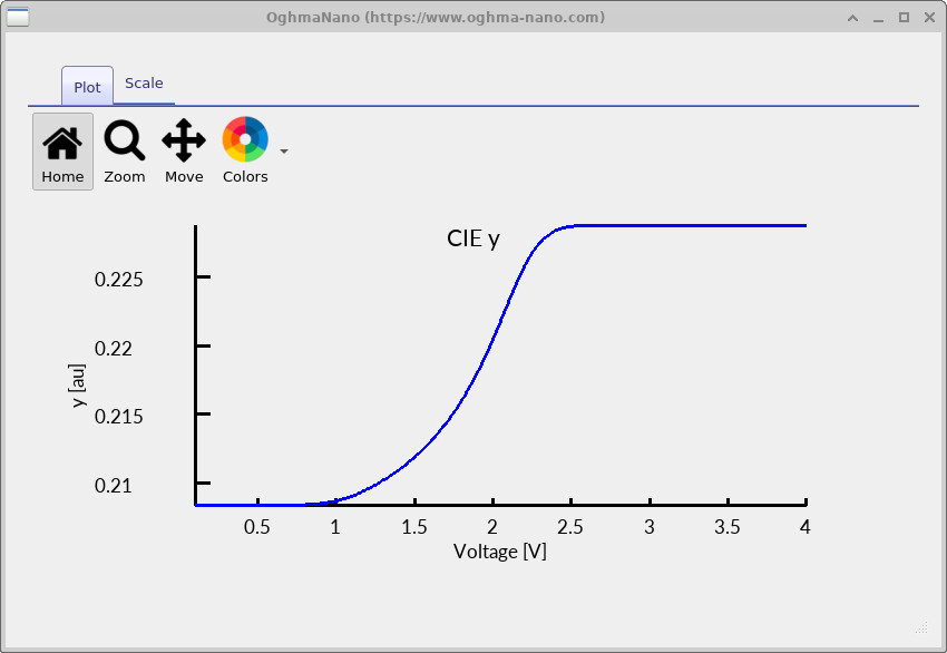
The colour used to plot the spectrum corresponds to the perceived output colour that an observer would see at that operating point. As the voltage is increased, this is visible directly in the graph as the plotted spectrum shifts from a lighter blue at low bias to a darker blue at higher bias, indicating a change in the emitted colour.
Finally, use the same snapshots workflow to inspect the EQE spectrum explicitly.
Plot eqe.csv and sweep the voltage slider to observe how the wavelength-dependent EQE changes with bias
(see ??).
In practice, the luminescence spectrum and EQE spectrum should be interpreted together:
the luminescence plot shows what is being emitted, while the EQE plot shows how efficiently each wavelength is coupled out at each operating point.
7. CIE colour space
OLED spectra are often reduced to a small set of perceptual colour coordinates so that colour stability can be assessed as a function of bias. The most common representation is the CIE 1931 system, where a spectrum is first converted to tristimulus values \((X,Y,Z)\) using the CIE colour-matching functions, and then normalised to chromaticity coordinates \((x,y)\).
Given a spectral power distribution \(P(\lambda)\) (for example, the emitted optical power per unit wavelength), the CIE tristimulus values are computed by weighting \(P(\lambda)\) with the colour-matching functions \(\overline{x}(\lambda)\), \(\overline{y}(\lambda)\), and \(\overline{z}(\lambda)\):
\[ X = k \int_{\lambda_1}^{\lambda_2} P(\lambda)\,\overline{x}(\lambda)\,d\lambda,\qquad Y = k \int_{\lambda_1}^{\lambda_2} P(\lambda)\,\overline{y}(\lambda)\,d\lambda,\qquad Z = k \int_{\lambda_1}^{\lambda_2} P(\lambda)\,\overline{z}(\lambda)\,d\lambda \]
Here, \(\overline{x}(\lambda)\), \(\overline{y}(\lambda)\), and \(\overline{z}(\lambda)\) describe the standardised spectral sensitivity of human vision, and the constant \(k\) is an overall scaling factor (its specific value depends on how \(P(\lambda)\) is defined and whether an absolute photometric calibration is being enforced). The corresponding chromaticity coordinates are then obtained by normalisation:
\( x=\dfrac{X}{X+Y+Z}, \qquad y=\dfrac{Y}{X+Y+Z} \)
The \((x,y)\) coordinates represent chromaticity (hue/saturation) largely independent of absolute brightness, which is
useful for separating “how bright” the OLED is from “what colour” it appears. In OghmaNano, the CIE values are
computed from the simulated emission spectrum at each voltage step and written to the sweep output so that colour drift
can be plotted directly against electrical operating point. To view these sweep files, double-click on the
sweep/ directory in the Output tab to open the sweep viewer
(??).
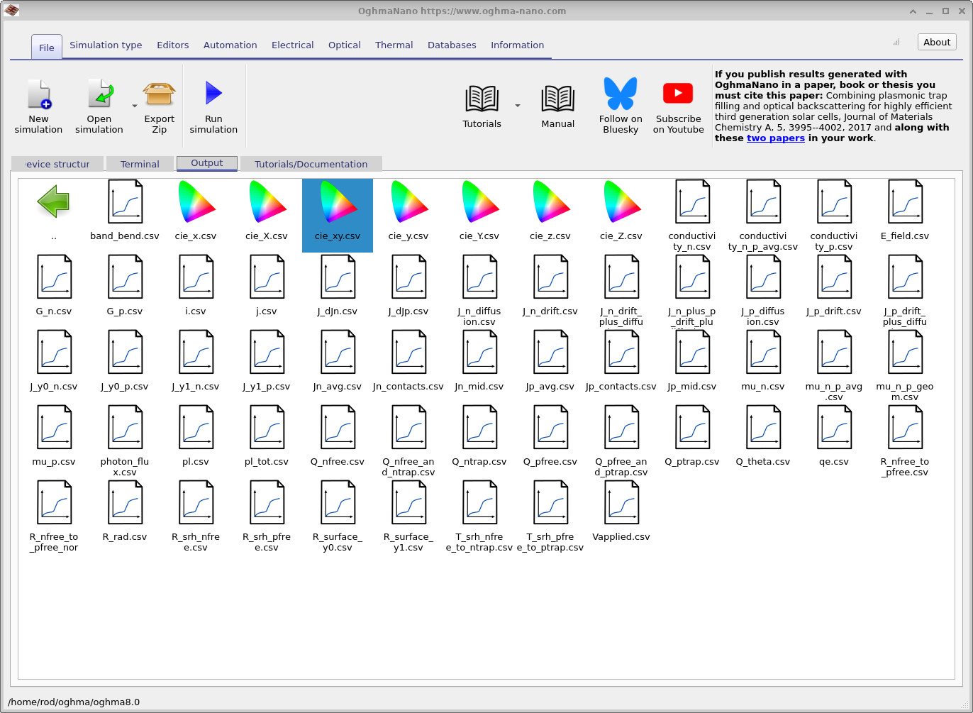
sweep/ directory where voltage-dependent CIE files are written.
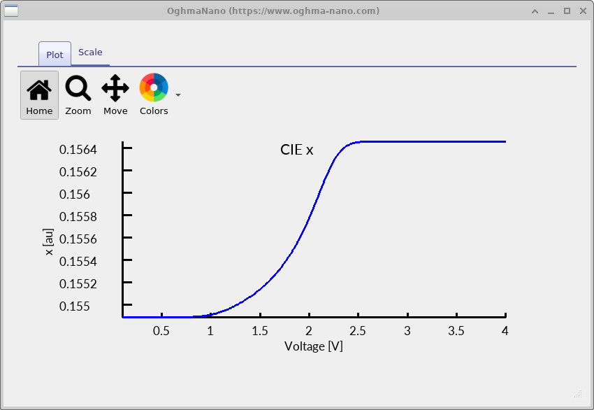
cie_x.csv).
cie_y.csv).
cie_xy.csv) as the voltage is swept.
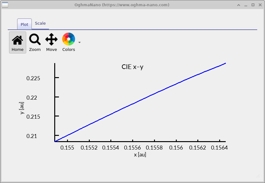
The figures above show how the simulated chromaticity evolves across the voltage sweep. The individual \(x(V)\) and \(y(V)\) curves (?? and ??) quantify colour drift as a function of operating point, while the \(y(x)\) plot (??) shows the same information as a path through chromaticity space.
In this example, the chromaticity moves systematically with increasing bias and then approaches a steady value at higher voltage. Physically, this typically reflects a change in the effective emitted spectrum with voltage (for example, due to a shift in the recombination zone within the optical cavity, or voltage-dependent spectral weighting from the outcoupling response). In well-optimised OLED stacks the corresponding \((x,y)\) drift is small;
8. Contacts
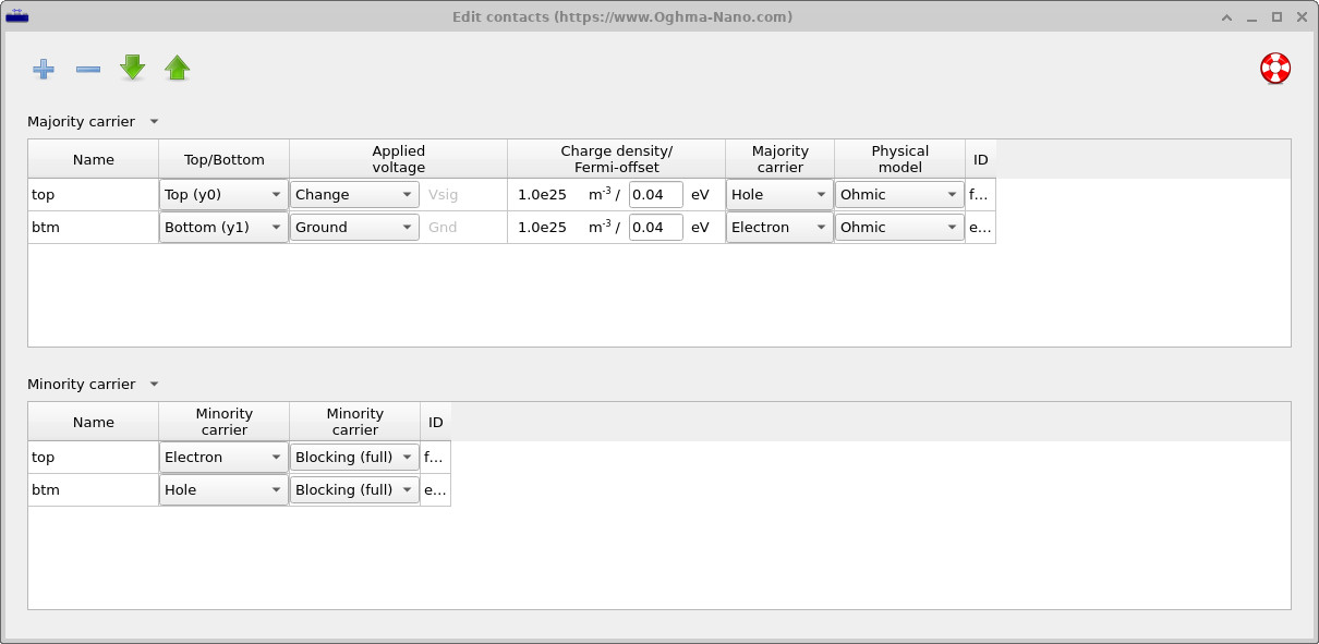
In this simulation, the OLED is treated as a well-designed device with efficient and selective electrical contacts. The contact boundary conditions are defined using the Contact editor, shown in ??, which is accessed from the Device structure tab in the main window.
The hole-injecting top contact and the electron-injecting bottom contact are both modelled as ohmic for their respective majority carriers. This means that charge carriers can enter and leave the device without an injection barrier, so that current flow is not limited by the contacts but by transport and recombination within the organic layers themselves.
Minority carriers are blocked at each electrode: electrons are blocked at the hole-injecting contact and holes are blocked at the electron-injecting contact. This enforces carrier selectivity and suppresses leakage currents, ensuring that electrons and holes are confined to their intended transport paths and recombine in the interior of the device.
With this contact configuration, the simulation operates in the bulk-limited regime appropriate to a high-quality OLED. The electrical response is therefore governed by carrier transport, spatial overlap, and radiative recombination in the emissive layer, allowing the internal device physics and its coupling to the optical cavity to bector be examined directly.
👉 Next steps:
- Continue to Part B to learn about ray tracing and angle-dependent emission.
- Explore the theory of singlets and triplets in OLED simulations .
- Return to the introduction to organic electronics for a broader overview of the topic.