Optical Filter Design Adjusting Layer Width Systematically: Part B
In this Part B of the tutorial, we will look at automatically scanning the filter widths. This allows you to design filters, scan them automatically, and study how the structure of the filter affects both transmission and reflection. By running systematic scans, you can quickly generate an overview of many different filter designs and choose the one that best fits your application.
Scanning filter widths
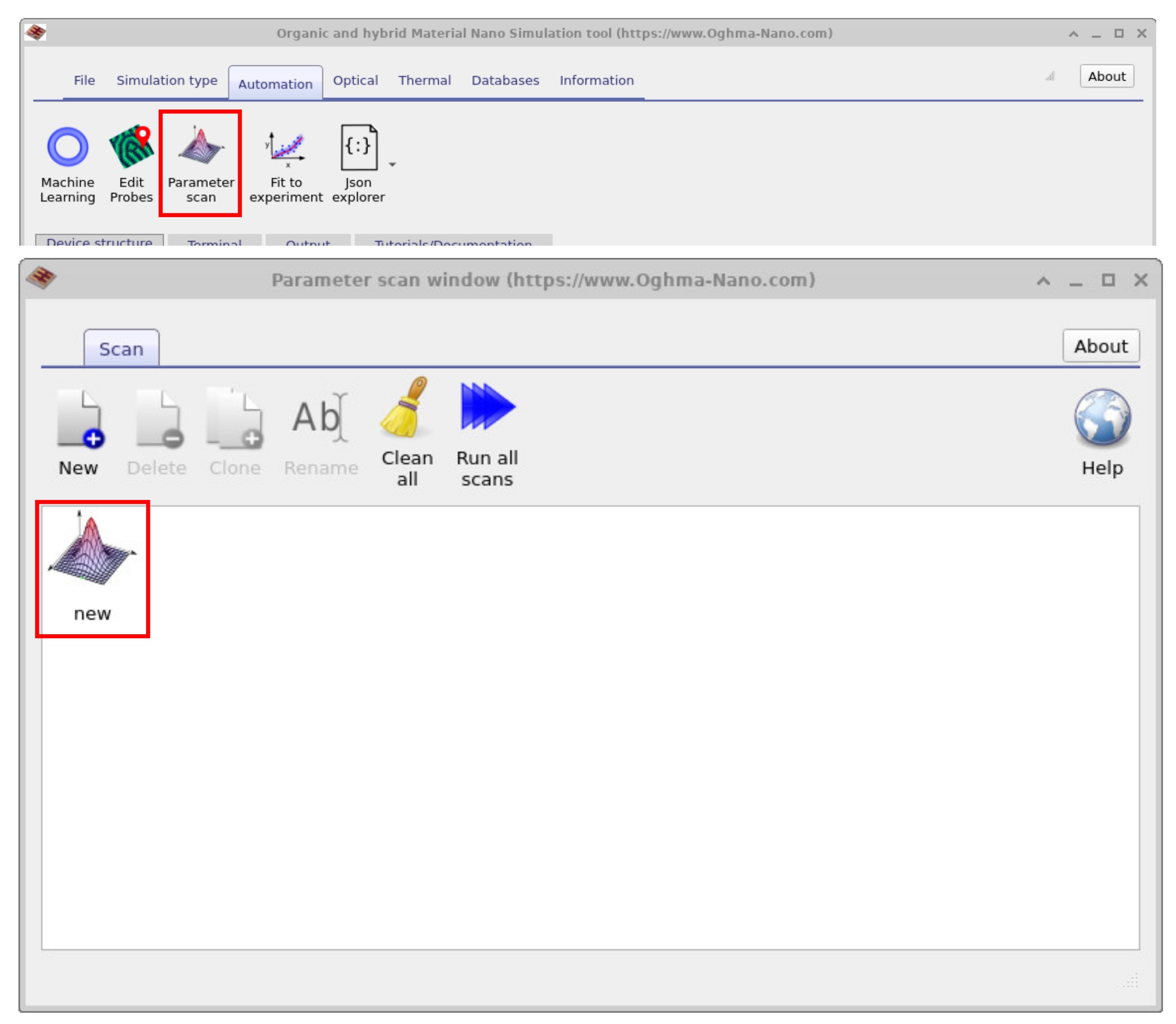
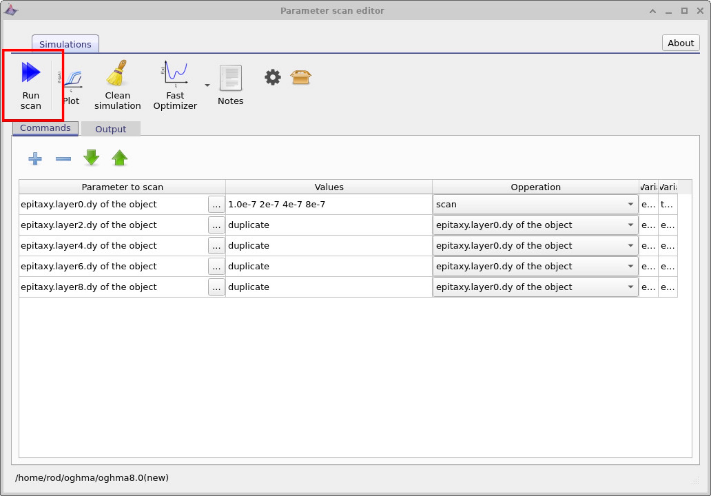
Navigate to the Automation ribbon in the main window and click on Parameter Scan (see ??). The Parameter scan window will open, and there should already be a new scan entry called new. Double-click on this entry, and the scan setup window will appear (see ??). Finally, click Run scan to start the calculation. The scan may take a short time to complete depending on the number of parameter values you selected.
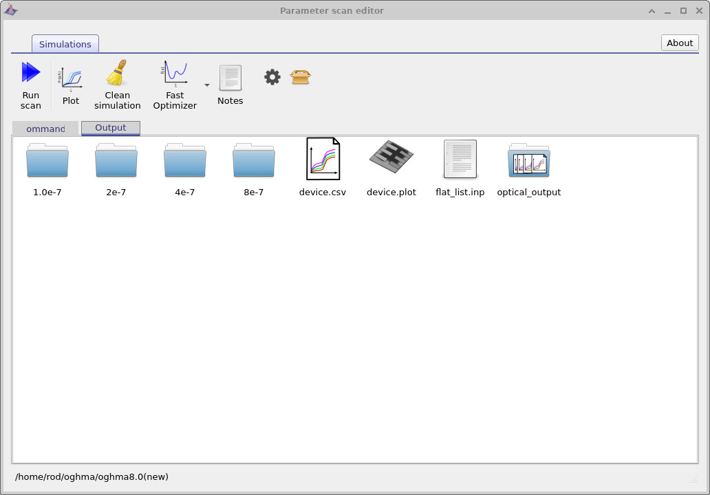
By clicking Run scan, you executed the small program shown in ??. We will explain this program later, but in essence it varies the thickness of the highest–refractive-index layer over a set of values. Open the Output tab in the Parameter Scan window (see ??): you will see four directories—each corresponds to one of the scanned thicknesses. Every directory contains a full simulation with the usual files, differing only in that layer’s thickness.
In the root of the scan folder you’ll also find special “multi-curve” icons (CSV files with a multi-line symbol).
These aggregate the corresponding curves from all sub-simulations.
Double-click optical_output to open it (see
??);
you’ll see reflect.csv and transmit.csv.
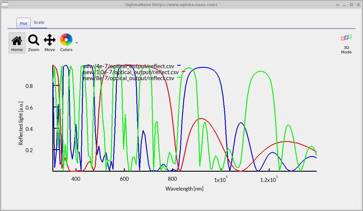
Opening reflect.csv plots the reflectance from all scanned thicknesses on one graph, as shown in
??.
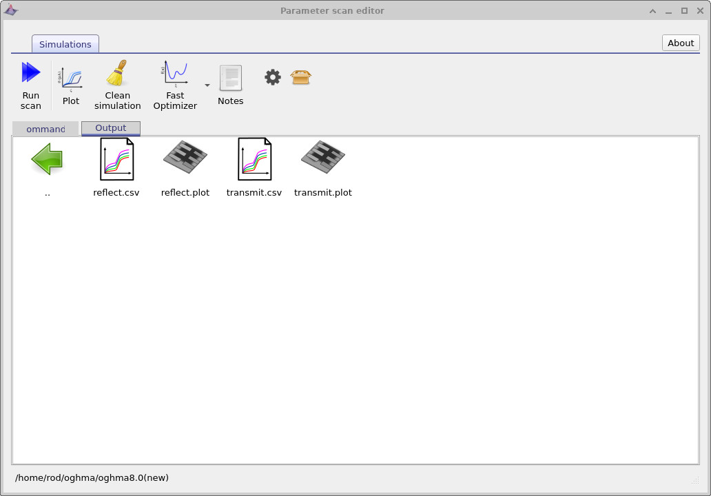
reflect.csv and transmit.csv.
Understanding the parameter scan window program
If you look again at
??,
you will see five rows listed. Each row specifies a
parameter to scan. In this example, the parameter is the thickness
(dy) of specific layers in the epitaxy stack. The entries are
epitaxy.layer0.dy, epitaxy.layer2.dy,
epitaxy.layer4.dy, epitaxy.layer6.dy,
and epitaxy.layer8.dy. These rows correspond to the
high refractive index layers in the device structure.
On the first line you can see a list of thickness values:
1.0e-7, 2e-7, 4e-7, 8e-7.
These are the values that the scan will assign to layer0.
The operation for this row is set to scan, which means the program will
systematically vary the thickness of layer0 across these specified values.
For the other layers (layer2, layer4,
layer6, and layer8), the operation is linked to
epitaxy.layer0.dy. In the values column this appears as
duplicate. This instructs the program to copy whatever value is currently set for
layer0 and apply it to the other high-index layers.
In effect, whenever layer0 changes, the other high-index layers automatically
update to the same thickness.
In summary, this program scans through a set of thickness values for one high-index layer and then duplicates that thickness across all the other high-index layers in the stack. The solver is run for each case, enabling you to explore how the filter performance varies as a function of layer thickness.
Summary
In this part of the tutorial you have learned how to automate optical filter design using parameter scans. You varied layer thicknesses systematically, duplicated parameters across multiple layers, and explored how these changes affect transmission and reflection. With these tools, you can now rapidly evaluate many possible filter designs and identify the structures that best suit your application.