

Perovskite Band Structure (8-band k·p) — Cubic CsPbX3, MAPbX3 and Mixed-Halide Alloys
1. Introduction
Metal halide perovskites such as CsPbI3, CsPbBr3 and MAPbI3 (MA = methylammonium, CH3NH3) are direct-gap semiconductors used in solar cells, LEDs and, increasingly, lasers. Many device questions — effective masses, carrier statistics, optical gain, phonon-limited mobility — depend on the band structure close to the band gap. First-principles (DFT) calculations describe this well but are too expensive to evaluate on the dense k-grids needed for transport and gain. The k·p method solves this: a small Hamiltonian, parameterised against DFT, reproduces the bands near the gap at negligible cost.
Perovskite bands are inverted relative to familiar III–V semiconductors. In GaAs the conduction band is s-like and the valence band p-like; in lead halide perovskites the valence band is s-like and the conduction bands are p-like, with strong spin–orbit coupling splitting them. The lowest conduction band is the spin–orbit split-off band, and the heavy and light electron bands lie about 1.4–1.5 eV higher. In the cubic phase the direct gap sits at the R point of the Brillouin zone rather than at Γ.
This tutorial uses the eight-band k·p Hamiltonian and parameter set of K. Gawarecki, M. Wiśniewski, M. Polak, R. Kudrawiec and M. Gładysiewicz, “Eight-band k·p description and material gain for selected cubic and pseudocubic perovskites,” Phys. Rev. Applied 22, 014058 (2024), doi:10.1103/PhysRevApplied.22.014058 (open version: arXiv:2306.08643). In that work the k·p parameters for six perovskites were fitted to hybrid-functional (HSE06) DFT band structures including spin–orbit coupling. OghmaNano ships these parameters as ready-to-use material files, so you can compute bands, scattering rates and carrier statistics for any of the six materials — and for mixed-halide alloys between them — without writing any code.
2. Making a New Simulation
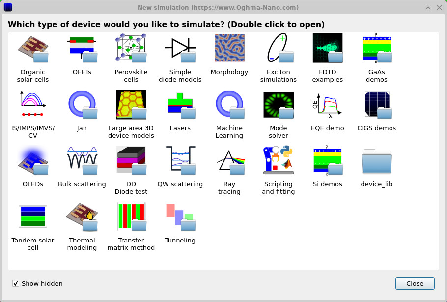
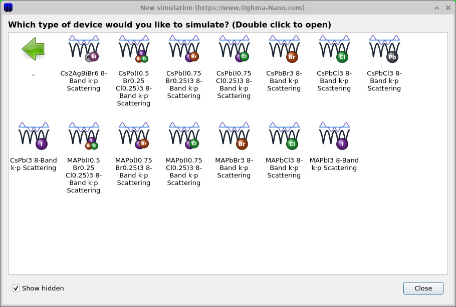
Click New simulation in the toolbar to open the simulation-type dialog (see ??). Double-click Bulk scattering. This opens a list of bulk perovskite demos, each labelled 8-Band k·p Scattering (see ??). Any of them can be used for this tutorial: the pure compounds (CsPbCl3, CsPbBr3, CsPbI3, MAPbCl3, MAPbBr3, MAPbI3) and several mixed-halide alloys. The screenshots below use CsPbCl3. Choose a location to save the simulation.
Once saved, the main window shows the device
(see ??):
a single CsPbCl3 (active) layer. Because this is a bulk calculation,
the structure is simply a slab of material; the thickness does not enter the bulk band structure.
Clicking Layer editor
(see ??)
shows a single 40 nm layer whose optical material is Generic/n/2.0. This is deliberate: the
optical constants play no role in the k·p band, scattering or mobility calculations, so a generic
placeholder is used.
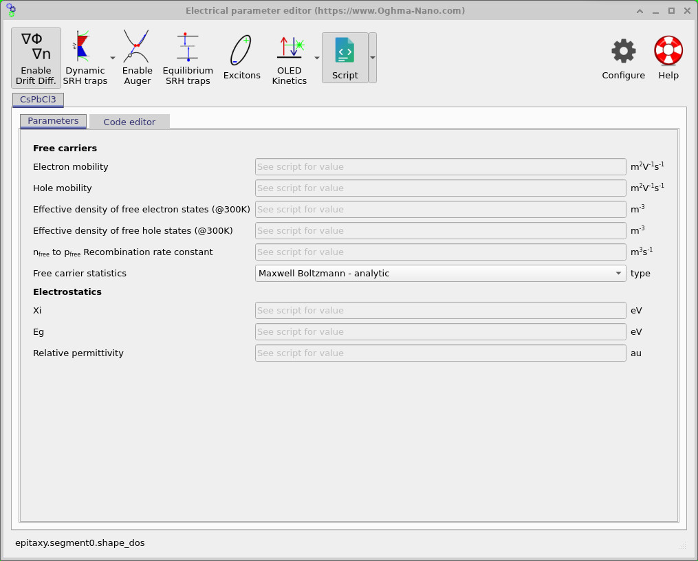
Next open Electrical parameters from the Device structure tab (see ??). The usual fields (mobility, effective density of states, Eg, χ, εr) are greyed out and read See script for value. In this simulation every material property is supplied by a material script rather than typed into the form.

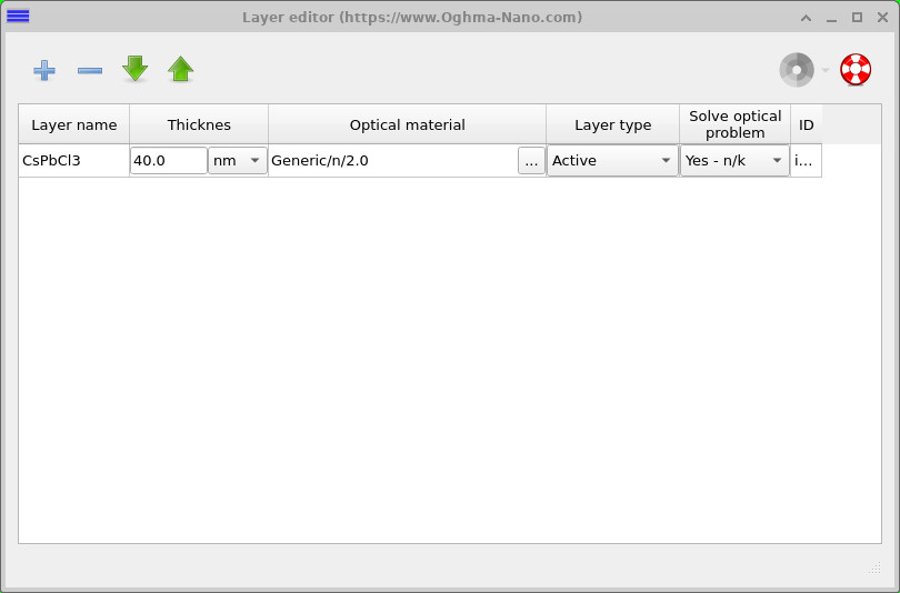
Generic/n/2.0 because optics does not enter the k·p calculation.
3. The material file and k·p parameters
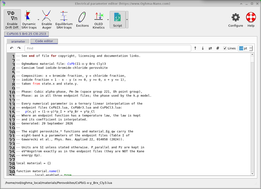
Click the Code editor tab in the electrical parameter editor to see the script
(see ??).
For this demo it is CsPbCl3.lua, stored in the OghmaNano materials library under
materials/Perovskites/. A material file is a Lua script: each property is a function
(for example material.epsilonr(state)) that returns a value and an enabled flag.
Because they are functions, properties may depend on temperature or on composition through the
state argument.
The header of the file records the physical assumptions. The crystal phase is the cubic α-phase (space group Pm-3m, Oh point group), which is the phase the k·p model describes. Note the caveat stated in the file: cubic CsPbCl3 is only the equilibrium phase above ~320 K (and cubic CsPbBr3 and CsPbI3 only above ~403 K and ~589 K respectively). Gawarecki et al. nevertheless use the α-phase for all materials so that they can be compared on an equal footing, and the material files follow the same convention.
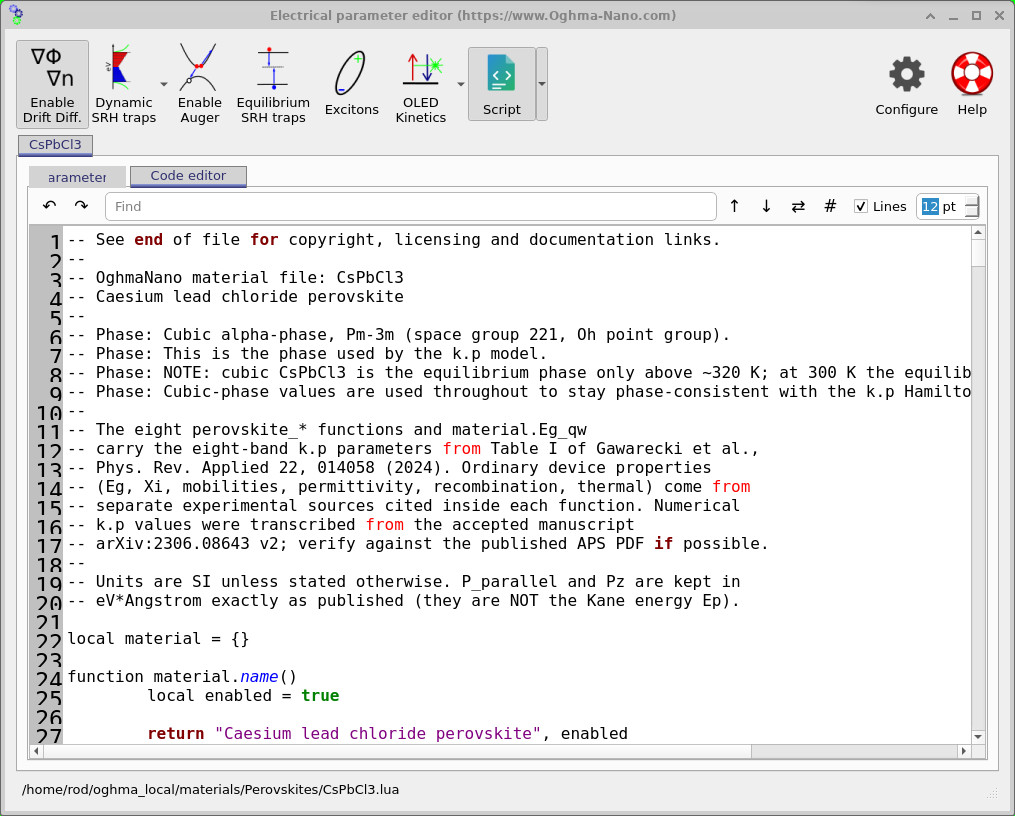
CsPbCl3.lua: crystal phase, parameter sources and unit conventions.

perovskite_gamma3_prime = −0.691, taken from Table I of Gawarecki et al.
Scroll towards the end of the file
(see ??).
Eight functions prefixed perovskite_, together with material.Eg_qw, carry the k·p
parameters. Each function cites its source — Table I of Gawarecki et al. — so that every number in
the simulation can be traced back to the literature. Ordinary device properties in the same file
(permittivity, mobilities, recombination, thermal parameters) cite their own separate experimental sources.
The eight-band Hamiltonian in brief
The eight-band model keeps the eight states closest to the gap (including spin): two s-like valence states (Γ6v+), two conduction states of the split-off band (Γ6c−) and four heavy/light-electron conduction states (Γ8c−). The Hamiltonian is written in block form \[ H = \begin{pmatrix} H_{8c8c} & H_{8c6c} & H_{8c6v} \\ H_{6c8c} & H_{6c6c} & H_{6c6v} \\ H_{6v8c} & H_{6v6c} & H_{6v6v} \end{pmatrix}, \] where the diagonal blocks describe each band on its own and the off-diagonal blocks couple them (Eq. (1) of Gawarecki et al.). At the R point (k = 0), with the valence-band maximum as the energy zero, the band edges are \[ E_v = 0, \qquad E_{sc} = E_g, \qquad E_{hc,\,lc} = E_g + \Delta_c \pm \frac{\delta}{3}, \] so Eg is the gap to the lowest (split-off) conduction band and Δc is the spin–orbit splitting of the conduction band. Away from R, the bands curve because of two contributions: the interband coupling P (the momentum matrix element between the s-like valence band and the p-like conduction bands), and the primed Luttinger-like parameters γ′1, γ′2, γ′3, which account for more remote bands outside the eight-band basis. For the cubic CsPbX3 compounds symmetry forces δ = ζ = 0 and P∥ = Pz. For the pseudo-cubic MAPbX3 compounds the orientation of the MA cation lowers the symmetry to C4v; δ then splits the heavy and light electron bands and ζ produces a small Rashba spin splitting. The full Hamiltonian is given in Section IV and Appendix A of the paper.
Two conventions in the material file are worth noting, as they are common sources of error when parameters are copied between codes:
- P∥ and Pz are stored in eV·Å, exactly as published. They are not the Kane energy EP, which is related by \(E_P = 2m_0P^2/\hbar^2\) (for CsPbCl3, EP ≈ 22 eV).
- The model uses the primed parameters γ′1–3. The unprimed γ1–3 also listed in the paper are derived quantities that already include the eight-band coupling; substituting them would double-count it.
The published parameters are reproduced in ??. The rows above the line are the inputs to the eight-band Hamiltonian; the rows below it are derived quantities listed for reference.
| Parameter | CsPbCl3 | CsPbBr3 | CsPbI3 | MAPbCl3 | MAPbBr3 | MAPbI3 |
|---|---|---|---|---|---|---|
| aexp (Å) | 5.605 | 5.886 | 6.294 | 5.675 | 5.901 | 6.329 |
| aDFT (Å) | 5.654 | 5.914 | 6.293 | 5.735 | 5.985 | 6.355 |
| Eg (eV) | 2.744 | 2.073 | 1.416 | 3.007 | 2.277 | 1.549 |
| Δc (eV) | 1.444 | 1.476 | 1.494 | 1.506 | 1.508 | 1.500 |
| δ (eV) | 0 | 0 | 0 | 0.045 | 0.057 | 0.075 |
| ζ (eV) | 0 | 0 | 0 | 0.016 | 0.030 | 0.045 |
| P∥ (eV·Å) | 9.233 | 8.948 | 8.601 | 8.878 | 8.623 | 8.097 |
| Pz (eV·Å) | 9.233 | 8.948 | 8.601 | 9.896 | 9.302 | 9.058 |
| γ′1 | 1.643 | 2.183 | 2.997 | 1.581 | 2.144 | 2.967 |
| γ′2 | 0.190 | 0.394 | 0.683 | 0.140 | 0.190 | 0.286 |
| γ′3 | −0.691 | −1.081 | −1.169 | −0.599 | −1.060 | −1.150 |
| mv (m0) | 0.189 | 0.158 | 0.125 | 0.210 | 0.178 | 0.141 |
| γ1 | 3.424 | 4.157 | 5.221 | 3.228 | 3.954 | 5.001 |
| γ2 | 1.081 | 1.381 | 1.795 | 0.963 | 1.094 | 1.302 |
| γ3 | 0.199 | −0.094 | −0.057 | 0.225 | −0.155 | −0.134 |
The derived valence-band mass is a useful sanity check on any parameter set. In the eight-band model it follows from the gap, the spin–orbit splitting and the interband coupling alone (Eq. (4) of the paper): \[ \frac{m_0}{m_v} = -1 + \frac{2m_0}{\hbar^2}\left[\frac{2P^2}{3(E_g+\Delta_c)} + \frac{P^2}{3E_g}\right]. \] For CsPbCl3, inserting Eg = 2.744 eV, Δc = 1.444 eV and P = 9.233 eV·Å gives mv ≈ 0.189 m0, matching the table. Light valence-band masses are one reason the iodides show the highest optical gain in the paper's comparison.
4. Swapping materials
To change the material, click the small arrow next to the Script button in the electrical
parameter editor and choose Import material script
(see ??).
This opens the materials library at materials/Perovskites/
(see ??).
Each .lua file is a complete material definition: CsPbCl3.lua,
CsPbBr3.lua, CsPbI3.lua, the methylammonium compounds (for example
CH3NH3PbCl3.lua) and the mixed-halide files CsPbI1-x-y_Brx_Cly3.lua and
CH3NH3PbI1-x-y_Brx_Cly3.lua.
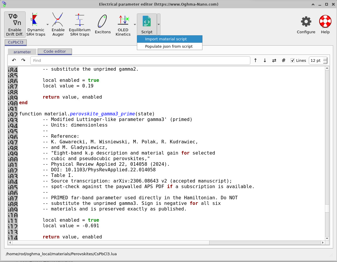
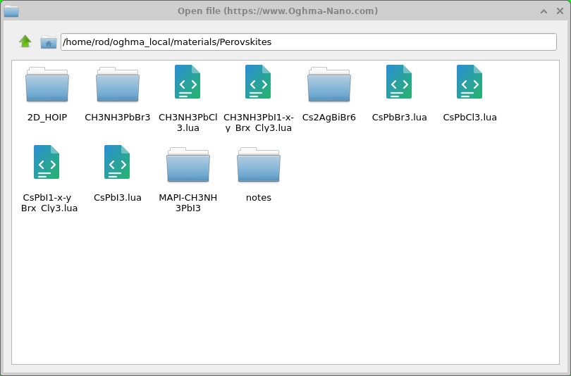
.lua file can be imported directly.
Double-clicking a script replaces the material definition of the layer, so every electrical and k·p property changes in one step. Because the script is then copied into your simulation, you are also free to edit it in the code editor — for instance to test the sensitivity of the results to a single parameter, or to enter a parameter set from a different paper. If you do, update the reference comments too, so the file stays traceable.
5. Mixed-halide alloys
Some of the material files describe mixed-halide alloys, CsPb(I1−x−yBrxCly)3 and its MA equivalent, rather than a single compound. Here x is the bromide fraction, y the chloride fraction, and the remainder 1 − x − y is iodide. The composition is set per layer in the Electrical ribbon by clicking Gradients/Strain (see ??), which opens the material gradient/strain editor (see ??).

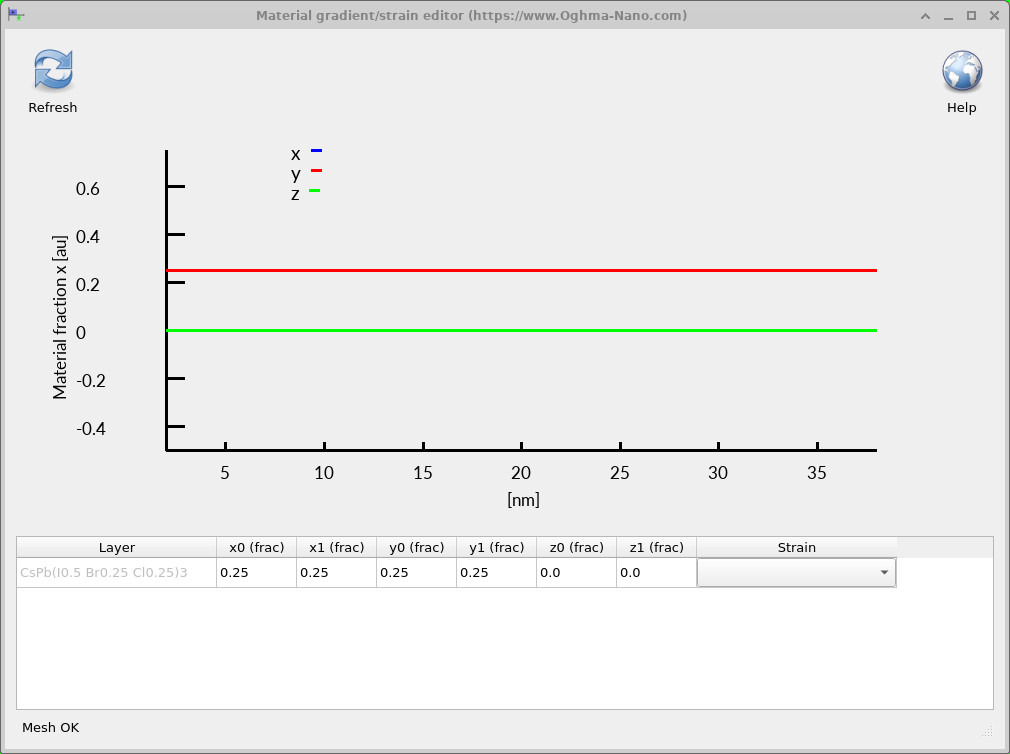
The table sets the fractions at the start (x0, y0, z0) and end (x1, y1, z1) of each layer, and the plot shows the resulting profile through the layer. For a bulk calculation you normally set start and end values equal, as in ??. Which fractions are meaningful, and what constraints apply, is defined by the material file itself; the rules are written in its header. For the mixed-halide files they are x ≥ 0, y ≥ 0 and x + y ≤ 1 (see ??). The z fraction is unused here.
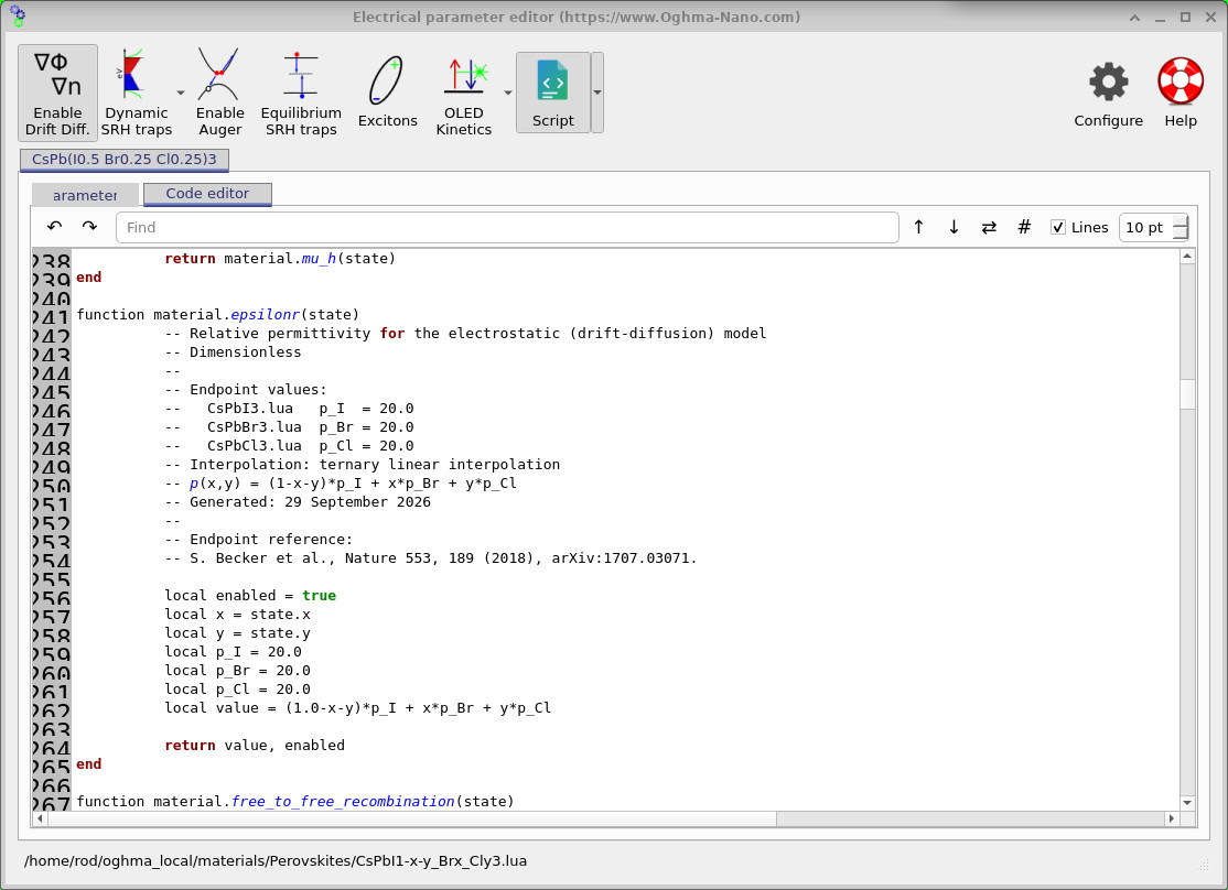
material.epsilonr interpolated between the three endpoint files using state.x and state.y.
Every numerical parameter in the alloy file is a ternary linear interpolation between the three
endpoint files CsPbI3.lua, CsPbBr3.lua and CsPbCl3.lua:
\[
p(x,y) = (1-x-y)\,p_{\mathrm{I}} + x\,p_{\mathrm{Br}} + y\,p_{\mathrm{Cl}}.
\]
Where an endpoint property has a temperature dependence, the functional form is kept and its coefficients are
interpolated. ??
shows this for the relative permittivity: the composition is read from state.x and
state.y and the three endpoint values are combined.
Linear interpolation is a first approximation. It ignores band-gap bowing and any local
disorder in real alloys, and it inherits the cubic-phase assumption of the endpoints. It is well suited to
exploring trends; for quantitative work on a specific composition, compare against measured band gaps and
add a bowing term to Eg in the script if needed.
6. Running the simulation and the band structure
Click Run simulation. The Terminal tab (see ??) first prints the k·p parameters actually used — the band structure (delta_c = Δc, delta = δ, zeta = ζ), the Kane coupling (P_parallel, Pz), the remote-band parameters (gamma1_prime … gamma3_prime) and the polar optical phonon parameters — followed by the progress of the scattering calculation. Checking this block is the quickest way to confirm the material is set up as intended.
The screenshot shows the CsPb(I0.5Br0.25Cl0.25)3 alloy, and the values can be verified directly against ??. For example, Δc = 0.5×1.494 + 0.25×1.476 + 0.25×1.444 = 1.477 eV and P = 0.5×8.601 + 0.25×8.948 + 0.25×9.233 = 8.846 eV·Å, exactly as printed.

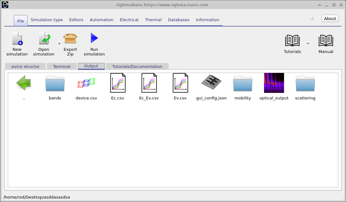
Ec_Ev.csv and the bands, scattering and mobility directories.
When the run finishes, open the Output tab
(see ??).
The individual bands are written to the bands directory; Ec.csv,
Ev.csv and Ec_Ev.csv collect them together (conduction bands, valence bands, and both).
Double-click Ec_Ev.csv to plot the band structure
(see ??).

Ec_Ev.csv for CsPb(I0.5Br0.25Cl0.25)3.
k is measured from the R point. Red: valence band; cyan: split-off conduction band at Eg;
upper pair: heavy and light electron bands at Eg + Δc.
The plot shows energy against wavevector measured from the R point, with the valence-band maximum at zero. Reading from the bottom:
- The valence band (red) curves downwards from 0 eV. It is s-like, so it is a single, spin-degenerate band — unlike the heavy-hole/light-hole pair in GaAs.
- The lowest conduction band (cyan) starts at ≈1.91 eV. This is the split-off band and Eg for this composition: 0.5×1.416 + 0.25×2.073 + 0.25×2.744 = 1.912 eV.
- The heavy and light electron bands start together at ≈3.39 eV (Eg + Δc) and separate as k increases because of their different curvatures. In the cubic material they are degenerate at R; in the MAPbX3 materials δ splits them by 2δ/3 even at k = 0.
The k range shown, up to 109 m−1 (0.1 Å−1), is roughly a fifth of the way from R to the zone boundary for a lattice constant of ~6 Å — comparable to the range over which Gawarecki et al. demonstrate close agreement between k·p and DFT (their Fig. 3). Much further from R, the eight-band model should not be relied upon.
7. Scattering, mobility and carrier statistics
With the bands known, OghmaNano evaluates polar optical phonon (Fröhlich) scattering. In ionic, soft lattices such as lead halide perovskites, coupling between carriers and longitudinal-optical (LO) phonons is the dominant intrinsic scattering mechanism at room temperature. Its strength is set by the LO phonon energy ℏωLO and by the difference between the high-frequency and static permittivities, both printed in the terminal (see ??). A convenient single measure is the dimensionless Fröhlich coupling constant \[ \alpha_F = \frac{e^2}{4\pi\varepsilon_0\hbar} \sqrt{\frac{m^*}{2\hbar\omega_{\mathrm{LO}}}} \left(\frac{1}{\varepsilon_\infty} - \frac{1}{\varepsilon_s}\right), \] which is large in perovskites because ℏωLO is small (here 18 meV) and ϵs is much larger than ϵ∞. The phonon parameters are not part of the Gawarecki et al. parameter set; they come from the separate sources cited in the material file. Scattering is outside the scope of that paper; it is OghmaNano using the k·p bands as the starting point for transport.
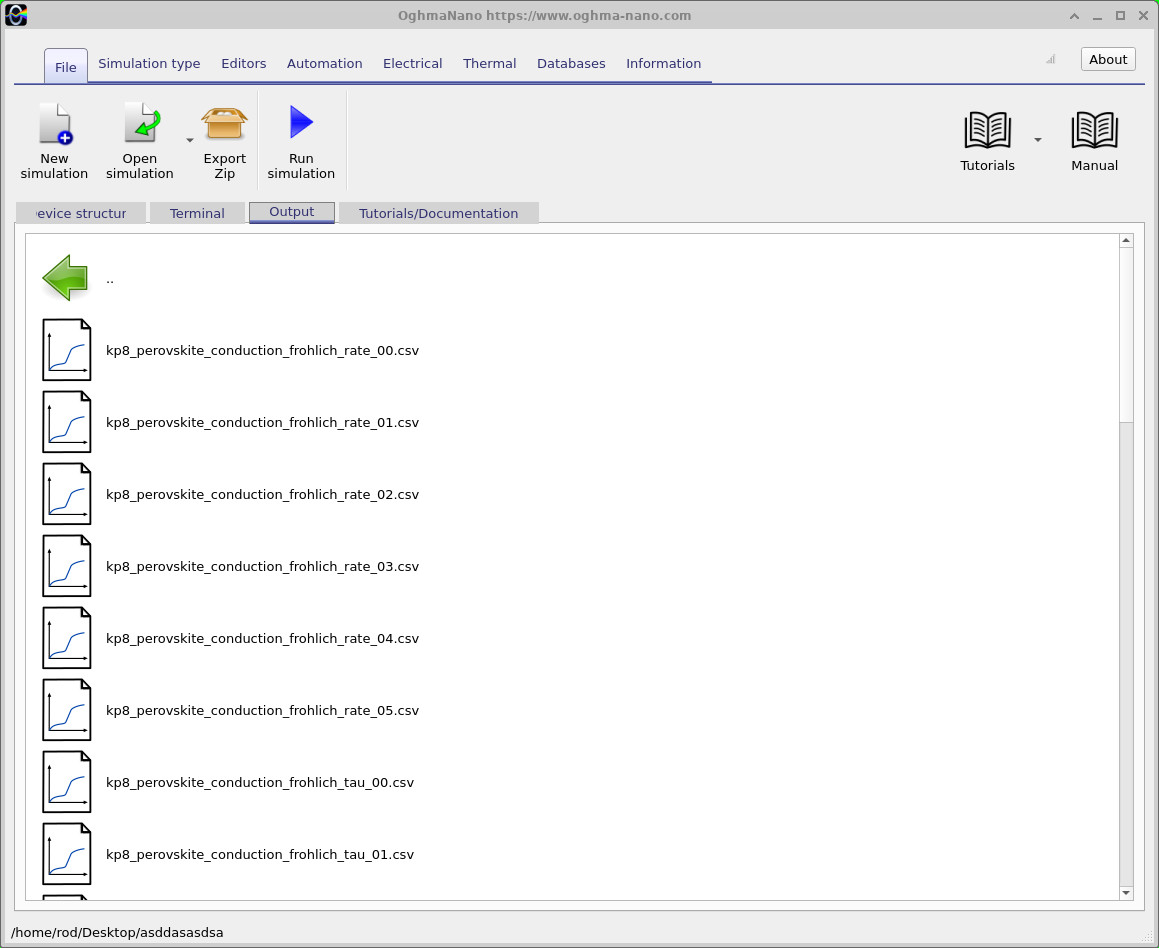
scattering directory: Fröhlich scattering rates and relaxation times, indexed by band.

kp8_perovskite_electron_fermi_level.csv.
Open the scattering directory
(see ??).
Files named kp8_perovskite_conduction_frohlich_rate_NN.csv give the scattering rate as a function
of energy, and kp8_perovskite_conduction_frohlich_tau_NN.csv the corresponding relaxation time
τ = 1/rate. The index NN runs from 00 to 05, matching the six conduction states of the eight-band model
(four from the heavy/light electron bands and two from the split-off band). The mobility directory
contains the carrier mobilities obtained from these scattering times together with the band curvature; in the
simplest picture \(\mu = e\langle\tau\rangle/m^*\), so light masses and weak scattering both raise mobility.
The k·p bands also fix the carrier statistics. ?? shows the electron Fermi level as a function of electron density, obtained by filling the calculated conduction bands. At low density it rises logarithmically, as expected for a non-degenerate semiconductor. Once it passes the conduction-band edge (≈1.91 eV for this alloy), at a density of order 1024 m−3 (1018 cm−3), the electron gas becomes degenerate and the Fermi level moves into the band. This is the same density range in which Gawarecki et al. find positive optical gain appearing in these materials (their Figs. 5–7), since gain requires the electron and hole quasi-Fermi levels to separate by more than the gap.