CELIV measurements on Perovskite Solar cells: Part a
1. Overview
In this tutorial we will begin by introducing the basic concepts of the Charge Extraction by Linearly Increasing Voltage (CELIV) technique, outlining how it is used to probe carrier mobility and density in thin-film semiconductors. After establishing the theoretical background, we will move quickly to practical steps, showing how to configure and run a CELIV simulation within OghmaNano. This combination of theory and hands-on simulation will provide both a clear understanding of the method and the tools to apply it to your own devices.
2. CELIV background
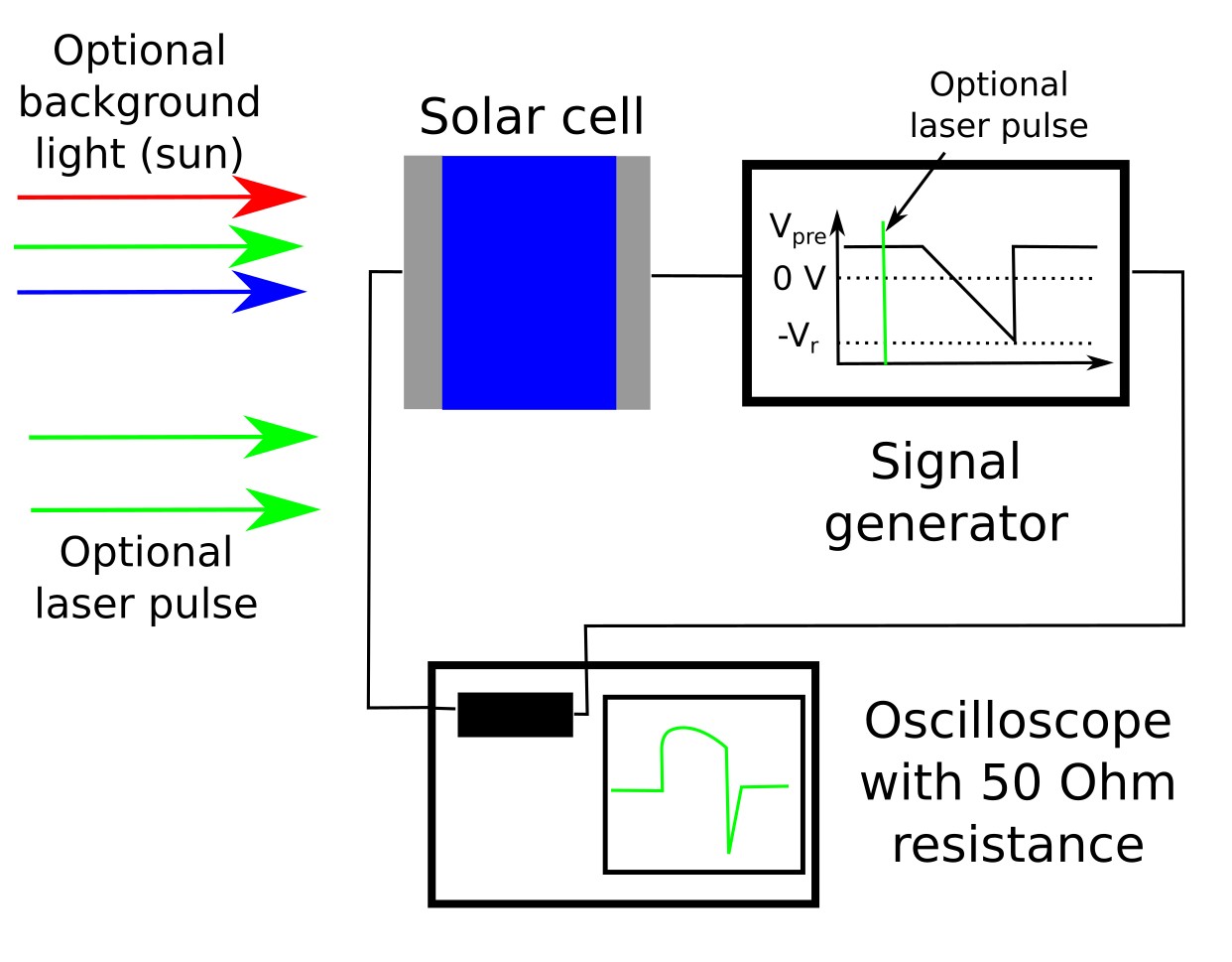
The Charge Extraction by Linearly Increasing Voltage (CELIV) technique is an experimental method used to study charge carrier mobility and density in organic and perovskite solar cells. In a typical setup, a solar cell is connected to a signal generator that applies a linearly increasing reverse bias, while the resulting current transient is recorded on an oscilloscope. Optional continuous illumination or a short laser pulse may be added to generate charge carriers. A schematic of this configuration is shown in ??.
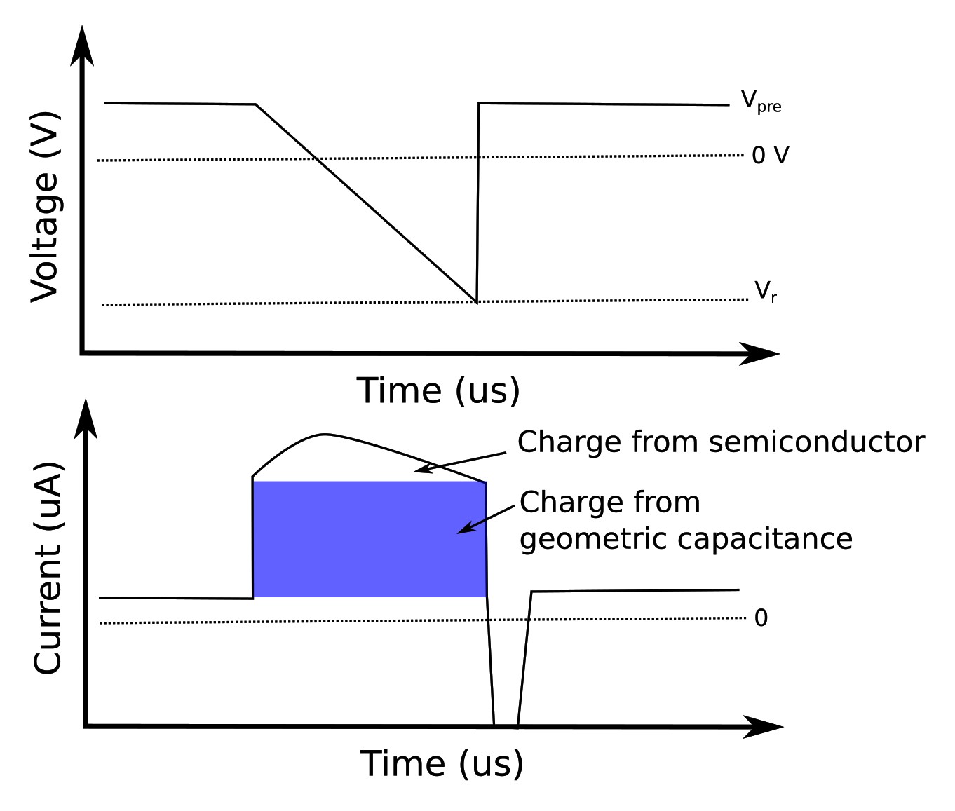
When the voltage ramp is applied, the measured current consists of two distinct contributions: a rectangular baseline from the device’s geometric capacitance and an additional peak from the extraction of mobile charge carriers in the semiconductor. The geometric capacitance term is always present, while the carrier-related peak provides direct information on mobility and carrier density. An example of these voltage and current transients is shown in ??.
The carrier mobility can be determined directly from the CELIV transient by measuring the time at which the extraction current reaches its maximum. In the simplest case of uniform carrier distribution and negligible recombination, the mobility is given by the CELIV equation: \[ \mu = \frac{2 d^{2}}{3 A t_{\text{max}}^{2}} \] where \(d\) is the active layer thickness, \(A\) is the voltage ramp rate (\(A = \mathrm{d}V/\mathrm{d}t\)), and \(t_{\text{max}}\) is the time at which the current peak occurs. This relation links the experimentally observed transient to the fundamental transport parameter of interest.
3. CELIV limitations
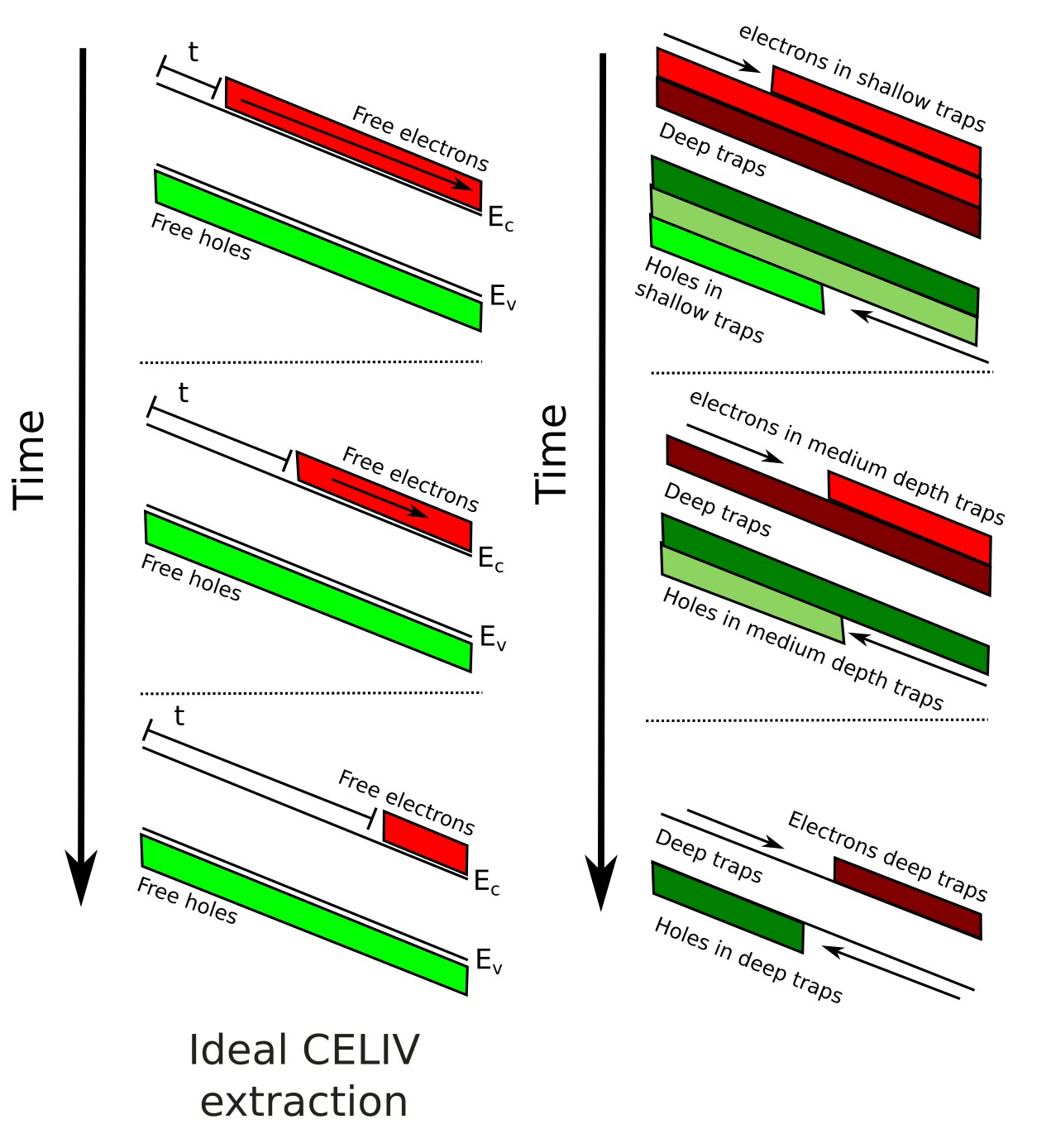
The derivation of the CELIV mobility equation relies on several simplifying assumptions. First, it is assumed that only one type of charge carrier dominates transport, so that only a single carrier species moves when the voltage ramp is applied. Second, carriers are assumed to be uniformly distributed, sliding smoothly out of the device in a manner similar to the idealized case shown on the left of ??. Third, recombination processes are considered negligible during extraction, so that no significant carrier loss occurs. In reality, these conditions are rarely satisfied. As illustrated on the right-hand side of ??, charge carriers often occupy shallow, medium, or deep traps, and their delayed release produces broadened or distorted extraction transients. As with many experimental techniques, the mobility extracted using CELIV should therefore be regarded as an approximation rather than the true microscopic value, and in fact the apparent mobility can evolve during the transient itself (doi:10.1063/1.4818267). This limitation is especially important in disordered organic semiconductors, where energetic disorder and trapping strongly affect transport. In contrast, perovskite materials often exhibit higher mobilities and lower trap densities, making the standard CELIV analysis more robust and easier to interpret.
💡 Test your understanding: Try applying the CELIV theory to a simple use case.
Suppose you have a device with thickness d = 200 nm,
a voltage ramp rate of A = 2 × 10⁶ V/s,
and a current peak observed at tmax = 5 µs.
Using the CELIV mobility equation, estimate the carrier mobility.
Show answer
The CELIV mobility is given by
\[
\mu = \frac{2 d^{2}}{3 A t_{\text{max}}^{2}}
\]
Substituting values:
d = 200 × 10-9 m,
A = 2 × 10⁶ V/s,
tmax = 5 × 10⁻⁶ s.
\[ \mu = \frac{2 (200 × 10^{-9})^{2}}{3 (2 × 10^{6}) (5 × 10^{-6})^{2}} \approx 1.1 × 10^{-4} \; \text{cm}^2/\text{Vs} \]
This simple example shows how the peak time in a CELIV transient can be converted into a mobility estimate.
4: Running a CELIV simulation on OghmaNano
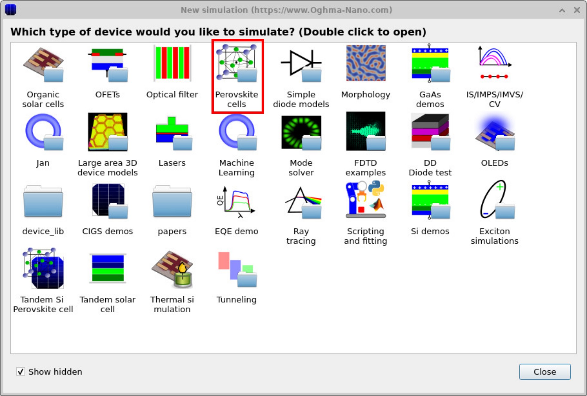
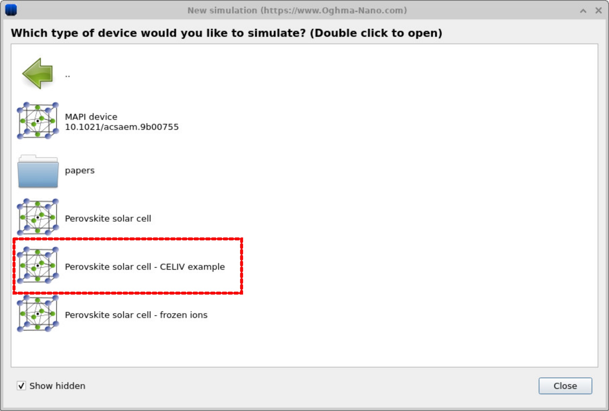
Click New simulation. This opens the library of available device types, shown in ??. Double-click Perovskite cells (highlighted in red) to open the perovskite examples folder. You’ll see a list of pre-set simulations, including MAPbI₃ device, Perovskite solar cell, and dedicated CELIV demos, as shown in ??. For this tutorial, select the Perovskite solar cell – CELIV example. When prompted, save the simulation to a folder where you have write access.
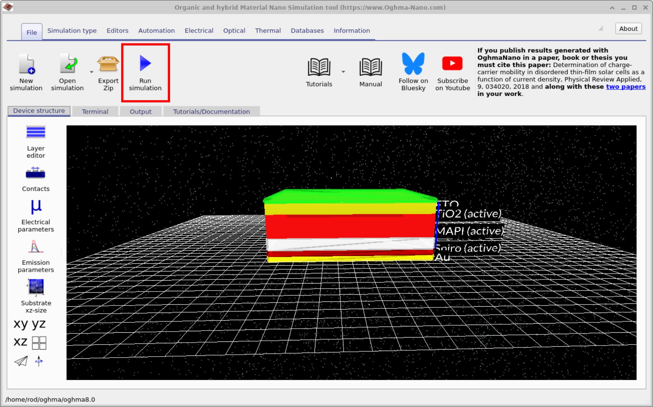
After selecting the Perovskite solar cell – CELIV example, the main simulation window opens (see ??). To start the calculation, click Run simulation (blue play icon) or press F9. OghmaNano will then solve the time-dependent drift–diffusion equations and generate the CELIV transient.
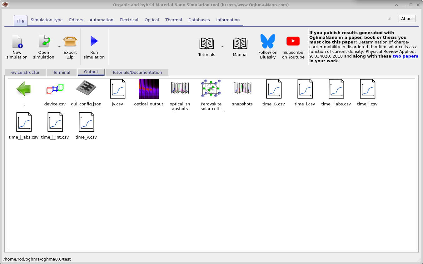
jv.csv (JV curve data), time_j.csv (extraction current vs. time),
time_v.csv (applied voltage vs. time), and optical_output (field distributions).
Double-click any file to view the corresponding results in the built-in plotting tools.
Step 5: View the CELIV results
Open the Output tab
(??)
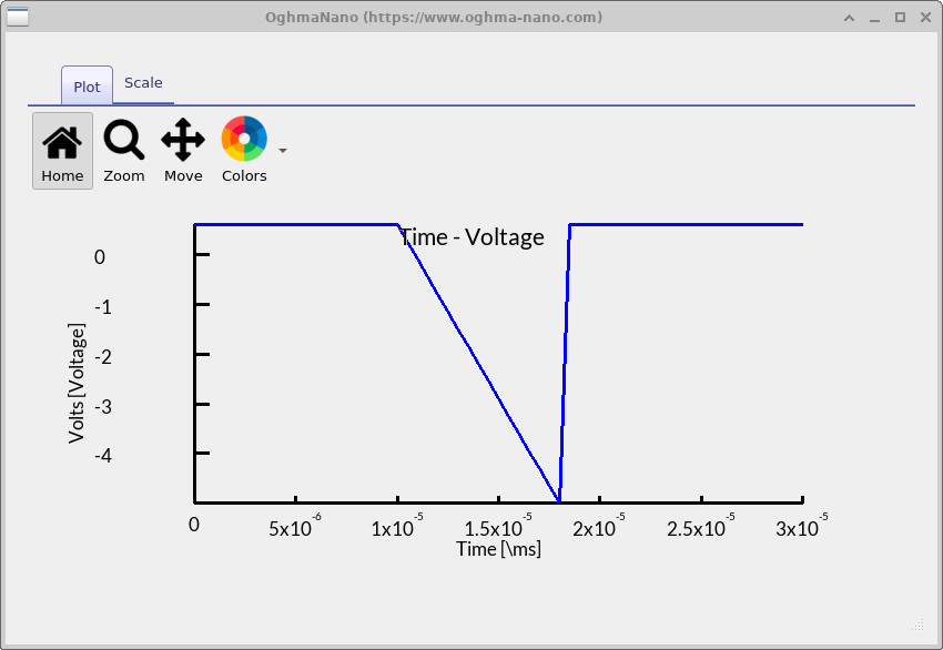
and double-click time_v.csv. This plots the applied voltage program —
the CELIV ramp — shown in
??.
Next, double-click time_j.csv to display the extraction current transient,
as in ??.
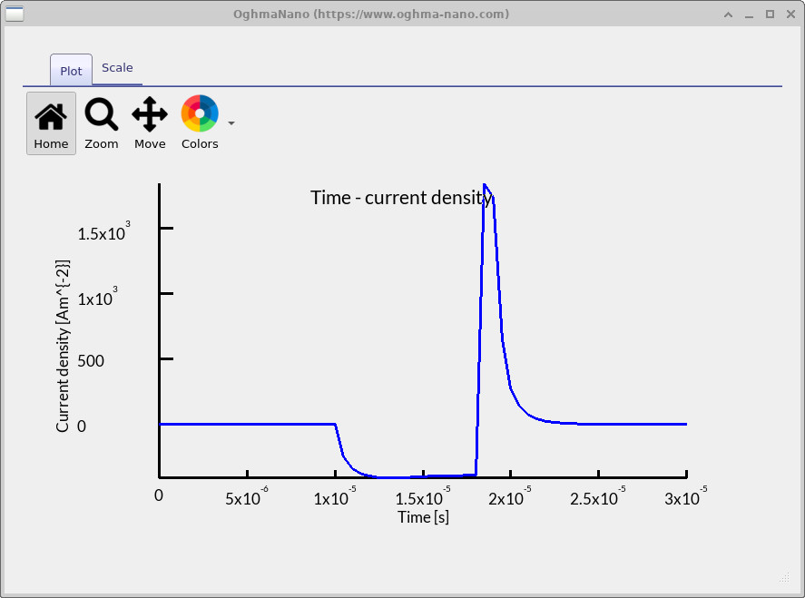
You’ll notice the transient has the familiar CELIV shape but appears **inverted**:
by sign convention in OghmaNano, current leaving the device is negative. When the ramp in
?? is applied,
charge is pulled out of the device, so the device delivers negative current (extraction peak).
The later peak of opposite sign (positive in
??) occurs when the bias
returns and charge rushes back into the device after the transient has returned to its initial state.
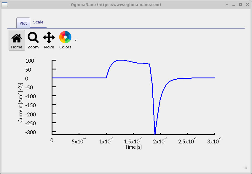
The plot in ?? shows the CELIV transient after multiplying the simulated current by –1 to match the conventional presentation used in experiments. In this form, the baseline corresponds to the geometric capacitance of the device, while the sharp positive peak indicates the extraction of mobile charge carriers during the applied voltage ramp. The magnitude and timing of this peak are the key quantities used to determine the carrier mobility and density. Presenting the transient in this conventional orientation makes it easier to compare OghmaNano simulations directly with published CELIV measurements. To extract the mobility, identify the time at which the current reaches its maximum (\(t_\text{max}\)) and substitute this value into the CELIV mobility equation \(\mu = \tfrac{2d^2}{3At_\text{max}^2}\), where \(d\) is the active layer thickness and \(A\) is the applied voltage ramp rate.
div style="clear: both;">🧪 Worked example: Read the CELIV peak time from
?? and estimate the mobility.
Assume an active layer thickness of d = 600 nm, a voltage ramp rate of
A = 5 × 10⁵ V/s, and a measured peak time of
tmax = 3 µs. What mobility do you obtain?
Show answer
Use the CELIV relation \[ \mu = \frac{2 d^{2}}{3 A t_{\text{max}}^{2}} \] with \(d = 600\times10^{-9}\,\mathrm{m}\), \(A = 5\times10^{5}\,\mathrm{V\,s^{-1}}\), \(t_{\text{max}} = 3\times10^{-6}\,\mathrm{s}\).
\[ \mu = \frac{2(600\times10^{-9})^{2}}{3\,(5\times10^{5})\,(3\times10^{-6})^{2}} \approx 5.3\times10^{-8}\ \mathrm{m^{2}\,V^{-1}\,s^{-1}} \] Converting to \(\mathrm{cm^{2}\,V^{-1}\,s^{-1}}\) (\(1\ \mathrm{m^{2}} = 10^{4}\ \mathrm{cm^{2}}\)): \[ \mu \approx 5.3\times10^{-4}\ \mathrm{cm^{2}\,V^{-1}\,s^{-1}}. \]
This value is in the typical range reported for disordered organic semiconductors. (If your \({t_\text{max}}\) changes with ramp rate or illumination, you’ll see \(\mu\) shift accordingly.)
👉 Next steps:
- Move on to the next CELIV simulation section — Part B — where we’ll adjust the voltage ramp rate, experiment with illumination intensity, and explore how changing electron/hole mobilities reshapes the CELIV transient.
- Return to the perovskite solar cell simulation guide for the full tutorial overview.