Solar Cell Simulation Software for OPV and Thin-Film PV Devices
1. Introduction
OghmaNano is a general-purpose solar cell simulation software platform for modelling thin-film photovoltaic devices including , organic photovoltaics (OPVs), perovskite solar cells and related structures such as silicon PN junction devices. It combines optical modelling with drift–diffusion transport and trap-state physics to provide a physically realistic description of device behaviour, with advanced characterisation techniques such as Suns–Voc analysis for diagnosing recombination mechanisms.
For disordered semiconductors such as OPVs, the simulator resolves thin-film optics, drift–diffusion transport, and non-equilibrium carrier trapping self-consistently, capturing how localized states influence charge transport, recombination, and electrostatics.
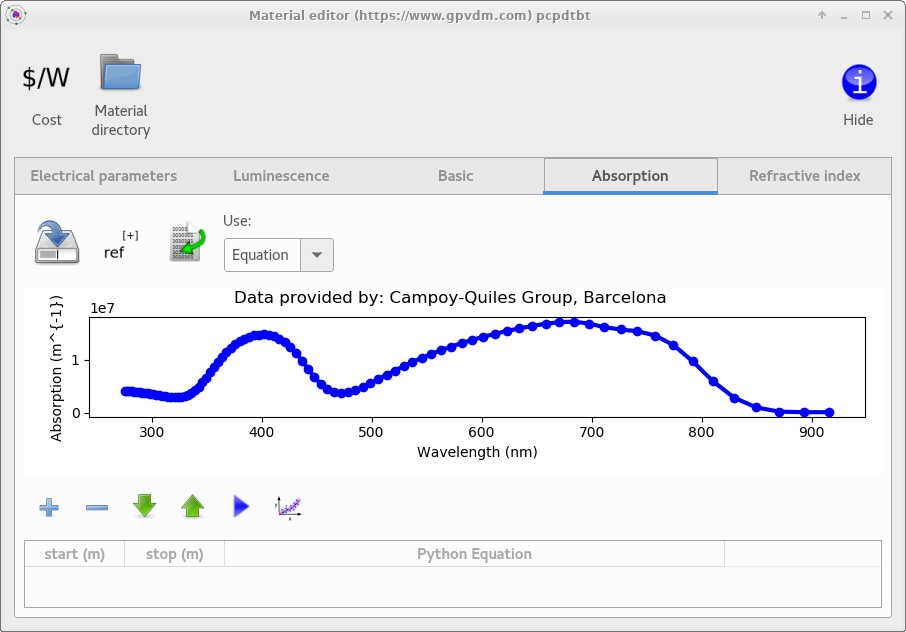
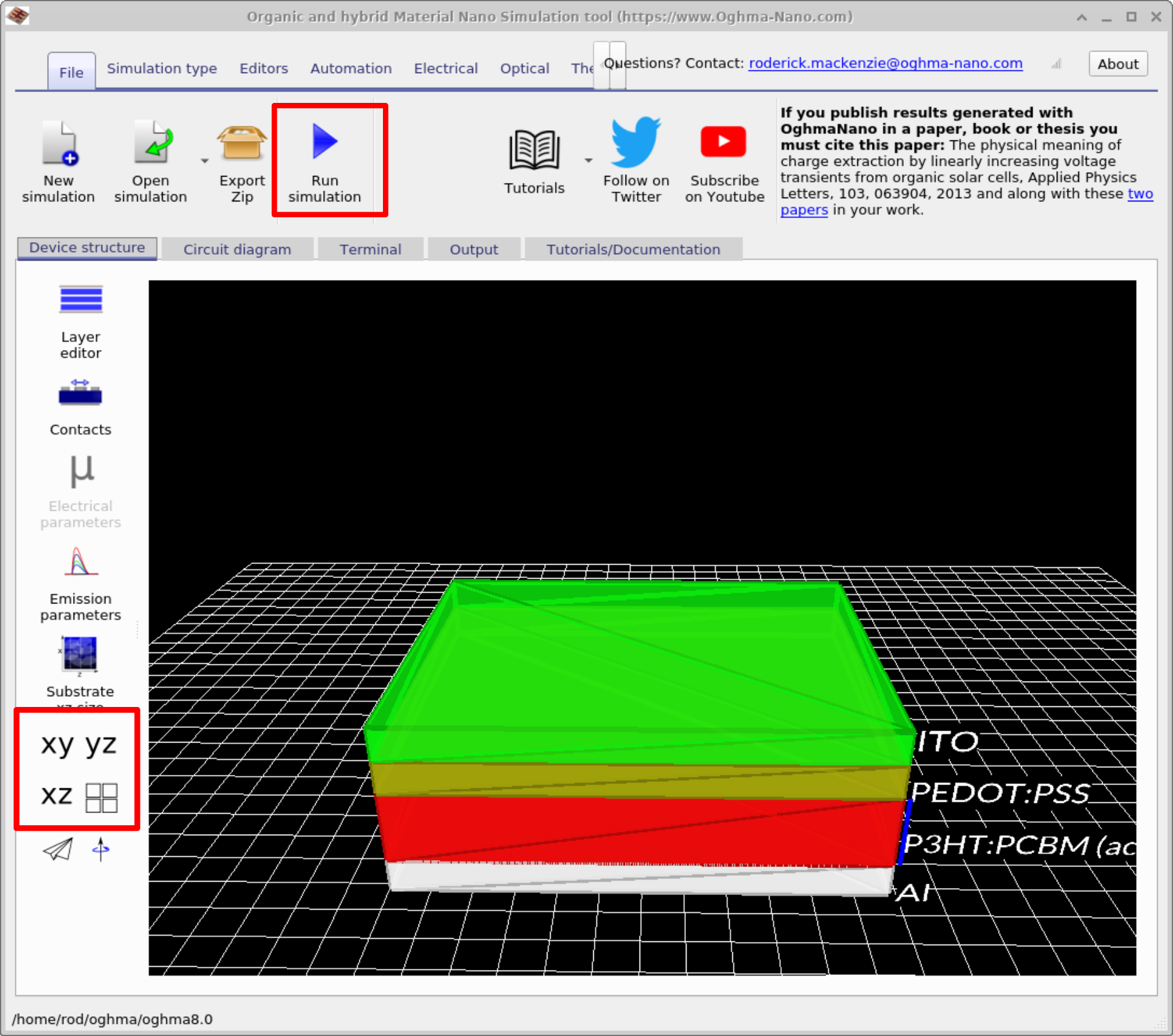
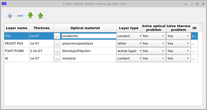
This unified approach allows light absorption, reflection, charge transport, trapping, recombination, energetics, and contacts to be resolved within a single model. Rather than simply fitting an equivalent circuit or reproducing a JV curve, OghmaNano makes it possible to understand why a device performs as it does and which physical processes are limiting performance. The main interface is shown in Figure ??, while the layer editor in Figure ?? is used to define the stack, materials, and thicknesses.
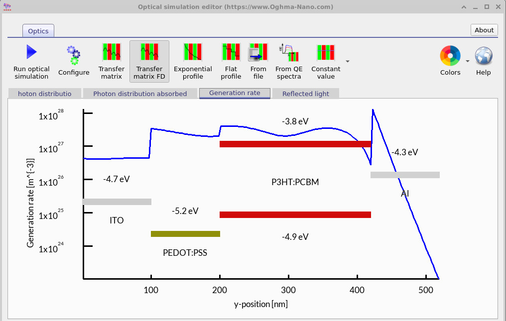
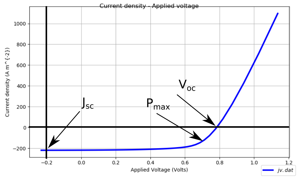
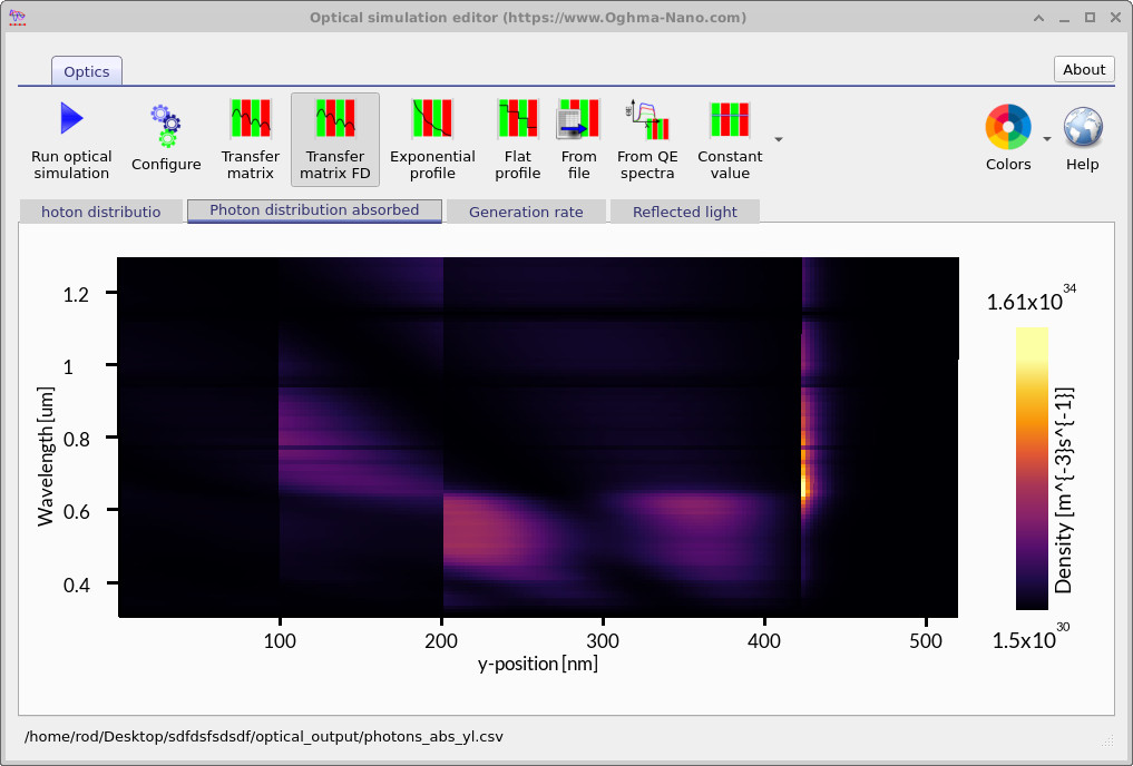
The same framework supports steady-state, transient, and frequency-domain simulations, including JV, TPV, CELIV, impedance spectroscopy, IMPS, and IMVS. Optical generation profiles can be calculated directly from multilayer thin-film optics, as illustrated in Figure ??, and the resulting electrical response analysed through outputs such as the JV curve shown in Figure ??.
Although this page focuses on OPVs, the same solver extends to perovskite solar cells, amorphous silicon structures, and large-area devices, including circuit-level models for studying spatial non-uniformities and scaling from individual cells to modules.
2. What you can do with OghmaNano
- Build realistic device stacks: define donor, acceptor, transport, interlayer, and electrode materials with spatially resolved properties.
- Model coupled optics and transport: combine thin-film optical calculations with full electrical device simulation.
- Include trap-limited physics: analyse how localized states, trapping, and trap-assisted recombination affect device performance.
- Visualise internal device operation: inspect fields, carrier densities, recombination, quasi-Fermi levels, and generation profiles in 1D, 2D, or 3D.
- Compare directly with experiment: simulate and interpret JV, TPV, CELIV, impedance spectroscopy, IMPS, and IMVS results.
- Understand loss mechanisms: separate optical, transport, trapping, and contact effects rather than folding them into empirical fitting parameters.
- Optimise virtually: perform parameter sweeps and explore device design changes before fabrication.
Try an OPV example.
Start with the quick-start OPV tutorial, then move on to optics and absorption, device structure and active layers, impedance spectroscopy, IMPS, IMVS, or large-area PM6:Y6 simulations.
3. The core OPV solver
To simulate OPV devices and other disordered solar cells, one begins with the standard drift–diffusion framework. This describes how charge moves through a device under the influence of electric fields and concentration gradients.
Electrons and holes are transported according to the drift–diffusion equations,
$$ \mathbf{J}_n = \mu_n n \nabla E_c + q D_n \nabla n $$ $$ \mathbf{J}_p = \mu_p p \nabla E_v - q D_p \nabla p, $$together with the continuity equations,
$$ \frac{\partial n}{\partial t} = \frac{1}{q}\nabla \cdot \mathbf{J}_n + G - R $$ $$ \frac{\partial p}{\partial t} = -\frac{1}{q}\nabla \cdot \mathbf{J}_p + G - R. $$The electrostatic potential is obtained from Poisson’s equation,
$$ \nabla \cdot \left( \varepsilon \nabla \phi \right) = -q \left( p - n + N_D^+ - N_A^- + \rho_{\mathrm{trap}} + \rho_{\mathrm{ion}} \right), $$which links the charge distribution to the internal electric field.
However, for OPV devices and other disordered semiconductors, this picture is incomplete. In these materials, a large fraction of charge resides in localized states, and recombination often occurs via these states rather than directly between free carriers.
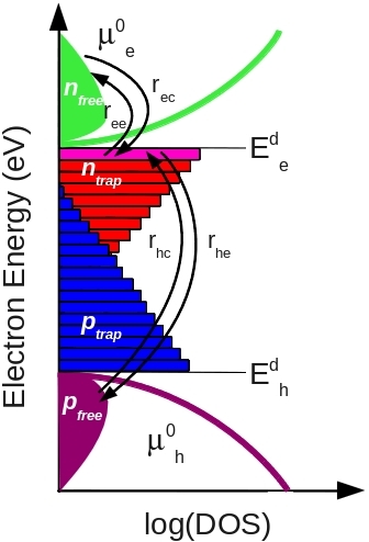
To describe this, OghmaNano includes explicit trap populations and solves a non-equilibrium form of Shockley–Read–Hall (SRH) recombination. The physical picture is shown in Figure ??: electrons and holes are captured into trap states and can later be re-emitted. Recombination occurs when carriers of opposite type meet through this trap manifold, providing an indirect pathway between the bands.
To describe recombination in disordered materials such as OPVs, OghmaNano does not start from a closed-form SRH expression. Instead, it begins from the underlying trap-state dynamics shown in Figure ??. Electrons and holes are continuously captured into and emitted from a distribution of localized states, forming a network of transitions between free and trapped populations.
For a given trap energy, the occupancy evolves according to
$$ \frac{dn_t}{dt} = r_{ec} - r_{ee} - r_{hc} + r_{he}, $$where \(r_{ec}\), \(r_{hc}\) are electron and hole capture rates into the trap manifold, and \(r_{ee}\), \(r_{he}\) are the corresponding emission processes. Recombination occurs when carriers of opposite type meet through these trap states.
The total trap-mediated recombination is therefore obtained by summing over all such transitions across the full density of states,
$$ R_{\mathrm{trap}} = \sum_i R_i \;\;\;\; \text{with} \;\;\;\; R_i \sim r_{ec,i} \cdot p_{t,i} \;\; \text{or} \;\; r_{hc,i} \cdot n_{t,i}, $$where each contribution \(R_i\) corresponds to recombination through a specific region of the trap distribution. If one assumes steady-state conditions and a single effective trap level, this full description reduces to the familiar Shockley–Read–Hall expression,
$$ R_{\mathrm{trap}} \sim \frac{np - n_i^2}{\tau_p (n + n_t) + \tau_n (p + p_t)}, $$but this simplified form does not retain the dynamic evolution of trap occupancy or explicitly track charge stored in traps. In disordered semiconductors, that trapped charge contributes directly to the electrostatics through Poisson’s equation, modifying the internal field and band bending. For this reason, OghmaNano solves the full dynamic trap system rather than relying solely on the analytical SRH limit.
By solving these processes self-consistently, the OPV solver does not just predict device performance, but explains why it changes. For example, reductions in fill factor may arise from trap filling, mobility imbalance, or contact barriers, while current losses may originate from optical absorption limits or inefficient extraction.