Large-area device simulation – Part B: Running the scan and interpreting resistance & voltage loss
Step 1: Run the scanning simulation
Start the scan by clicking Run simulation (blue triangle) or pressing F9. The terminal output will begin to stream (see ??).
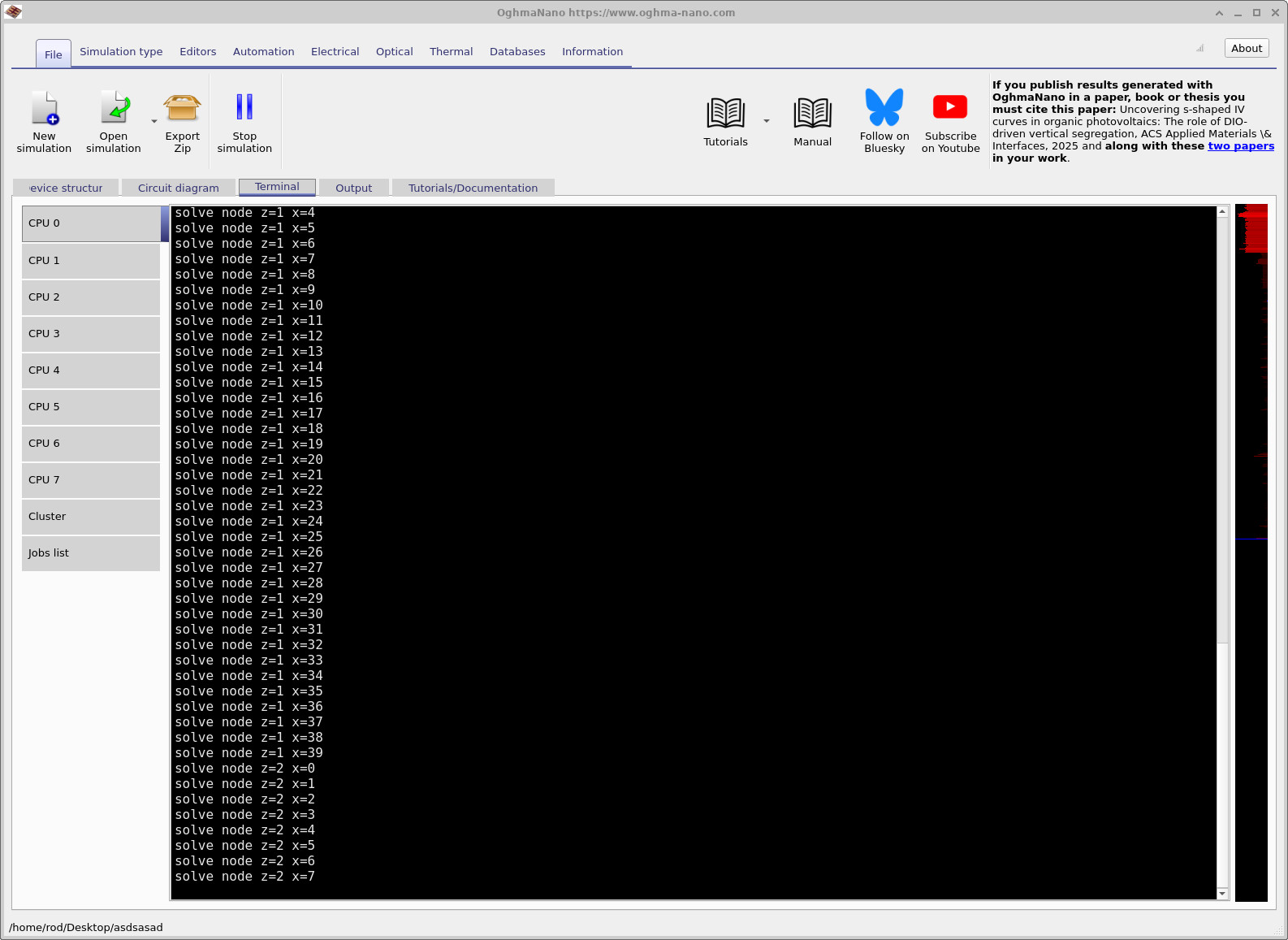
What is happening physically is simple: OghmaNano is treating the contact as a 3D resistive network. It then applies a voltage excitation at one mesh point on the bottom surface, solves the circuit, extracts an effective resistance to the top extraction contact, and repeats this for the next point.
For a 40 × 40 scan, this means 40 × 40 = 1600 separate circuit solves. This is why the scan can take a while. You are not running a single JV sweep; you are running many small DC solves to build a spatial map.
💡 Practical note: If you increase the scan resolution substantially, runtime rises roughly with the number of scan points. Higher resolution gives you a cleaner map, but costs time.
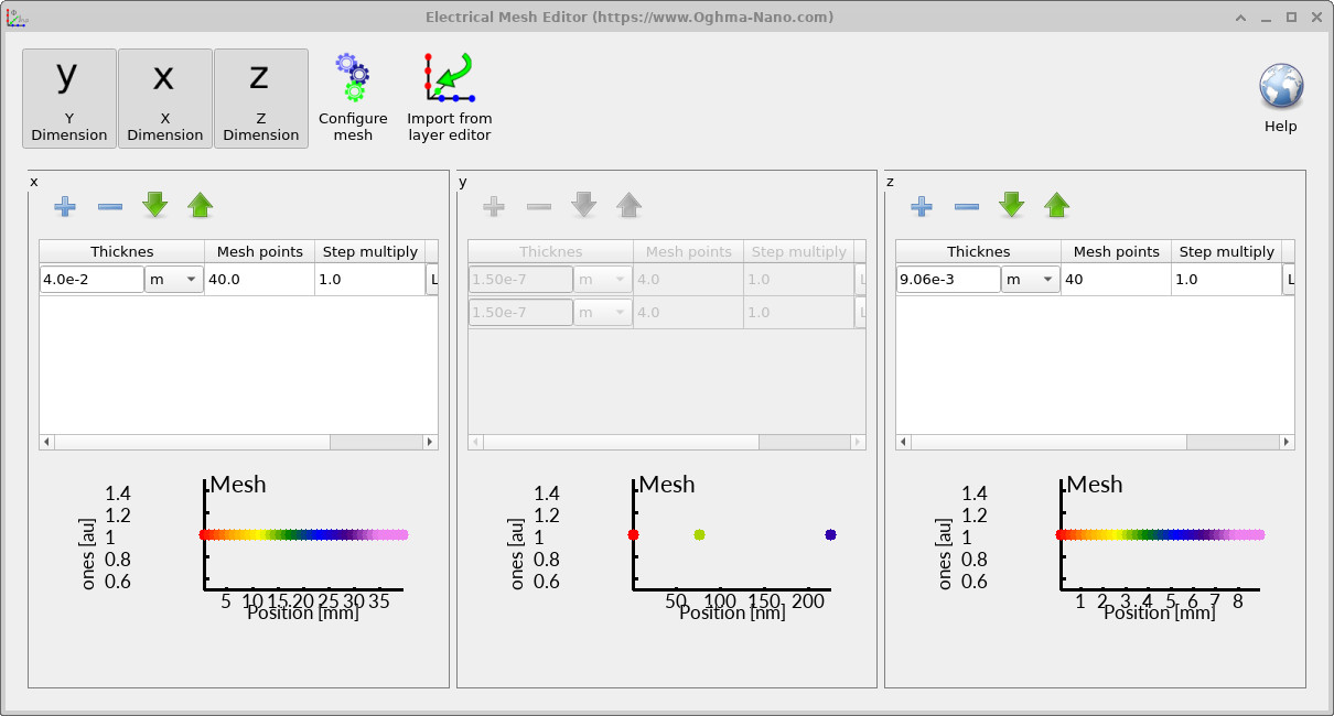
Step 2: Understanding the electrical mesh
The scan resolution is controlled by the electrical mesh, defined in the Electrical tab under Electrical mesh (see ??). In this example we use 40 × 40 points in the x–z plane. The y-direction is set by the layer stack (i.e. the solver knows the vertical discretisation from the layers you define).
As a rough guide:
- Too few points → the resistance map becomes blocky and you can miss fine-scale current crowding around the mesh.
- Too many points → the scan can become slow because the number of circuit solves increases.
Step 3: Output files produced by the scan
When the scan finishes, go to the Output tab. You should see files like those in ??.
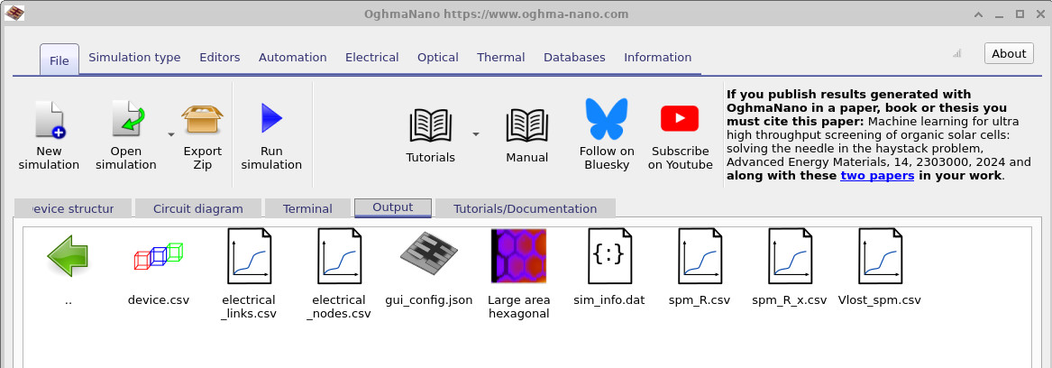
spm_R.csv), its slice (spm_R_x.csv), and the voltage loss map (Vlost_spm.csv).
| File name | Description |
|---|---|
electrical_links.csv | List of resistive links (edges) in the 3D circuit mesh |
electrical_nodes.csv | List of circuit nodes (positions and connectivity) in the 3D mesh |
spm_R.csv | Scanning probe microscopy resistance map (effective resistance vs position) |
spm_R_x.csv | 1D slice through spm_R.csv showing resistance across the device |
Vlost_spm.csv | Estimated voltage loss (ΔV) at each scan point due to contact resistance |
Step 4: Viewing the resistance maps and slices
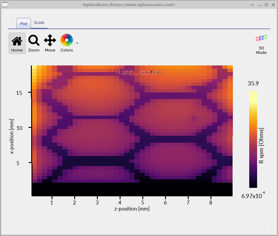
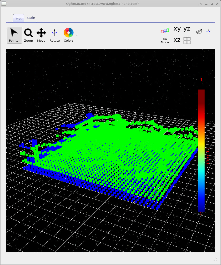
spm_R.csv). Low resistance occurs near the extraction bar and
metallic mesh lines; the highest resistance is typically deep inside a cell, far from both.
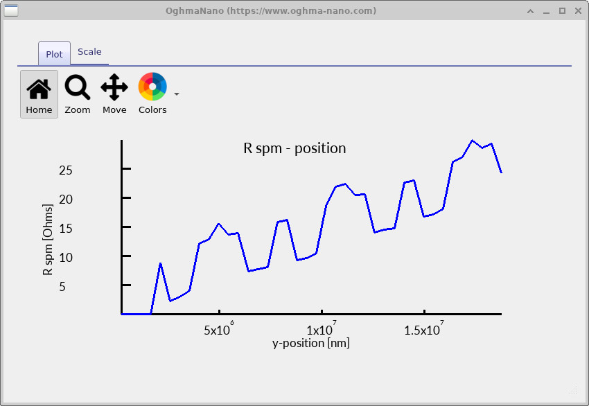
spm_R_x.csv. Resistance increases with distance from the
extraction edge, with periodic drops where the slice passes close to metallic mesh segments.
Double-click spm_R.csv to view the resistance map (see ??). The colour scale represents the effective resistance between each bottom-surface point and the extraction contact.
- Close to the extraction contact (the dark bar in the plot), the resistance is lower – current has a shorter path to leave the device.
- Close to a metallic mesh line, the resistance is lower – current can quickly enter the highly conducting metal network.
- The highest resistance tends to occur near the centre of a mesh cell and far from the extraction edge, because current must travel laterally through the polymer for a longer distance.
In this example the resistances are on the order of ohms, which is a physically sensible scale for current-spreading in printed contacts. However, note that values approaching a few tens of ohms are not benign for many devices: a 30–40 Ω path from the active region to the external contact can severely reduce effective fill factor (PV) or cause brightness non-uniformity (OLED).
Double-click spm_R_x.csv to view a 1D slice through the map (??). This plot makes the physics explicit:
- Resistance increases as you move away from the extraction contact (longer lateral current path).
- Resistance drops whenever the scan passes over or near a metallic mesh line (short-circuiting the lateral path).
This is the key diagnostic: it tells you not only how bad the contact is, but where it is bad, and therefore what geometric/material modification would fix it.
Step 5: Visualising the circuit mesh (links and nodes)
For debugging and interpretation it can be useful to visualise the circuit representation directly. Double-click the link and node visualisations (often presented as links.jpg and nodes.jpg in the example output).
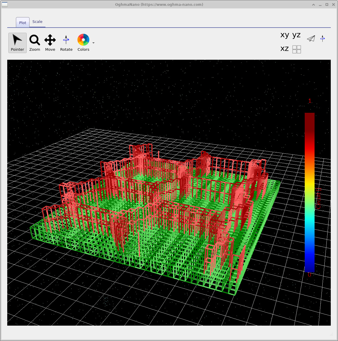
In these contact problems the circuit interpretation is literal: each link is a resistor, each node is a junction, and the solver is enforcing Kirchhoff’s laws across the network.
Step 6: Configuring the scan (Scanning Probe Microscopy editor)
The scan you just ran is configured using the Scanning Probe Microscopy (SPM) editor. You can open it from the editor ribbon (see ??).
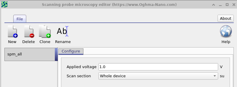
The configuration window (??) lets you choose the applied voltage and whether the scan covers the whole device or a subset. Subsets are useful for fast iteration when you only care about a particular region.
Step 7: Editing material resistivity (and why it matters)
To explore design trade-offs, you can edit the electrical parameters of each conducting layer. In the Device structure tab click Electrical parameters to open the electrical parameter editor (??). Here you can enter measured resistivities for your own materials and immediately predict how a scaled-up contact will behave.
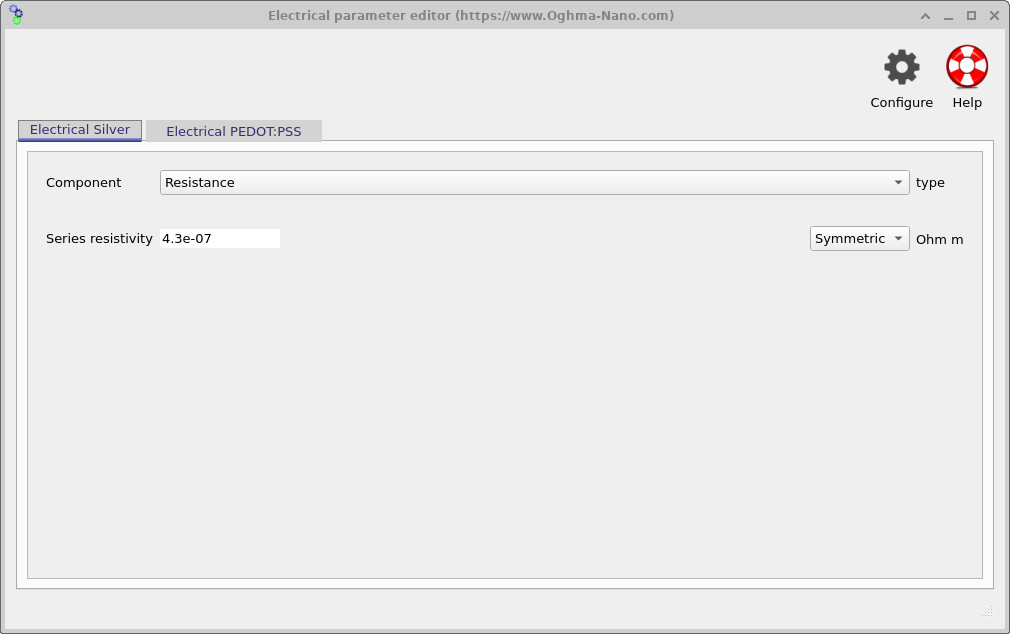
This type of parametric exploration is precisely the point of modelling: you can quantify whether a better polymer, a denser mesh, or a different extraction layout gives you the biggest performance gain before committing to fabrication.
👉 Next step: Continue to Part C to edit the contact geometry (mesh pitch, line width, extraction layout) and optimise performance.