Large-Area Device Simulation – Part C: Editing the Contact Geometry (Shape and Size)
In Part B, we kept the contact geometry fixed and examined how resistive losses depend on material properties and scan settings. However, in practice the most powerful parameter under your control is the geometry: the mesh pattern, its pitch, its line width, and the size of the device it must cover.
In this part, we will change the physical structure of the contact. This includes switching between different honeycomb patterns, editing the dimensions of the underlying mesh, and changing the size of the simulated substrate.
💡 Tip: If you want to generate your own mesh patterns from 2D images (for example from a printed mask, microscope image, or CAD output), see /manual/tutorial-shape-db-part-a.html. This is the same method used to populate the Shape Database referred to below.
Step 1: Open the Object Editor for the metal mesh
In the 3D view, right-click on the hexagonal metal mesh and choose Edit object (see ??). This opens the Object Editor (??).
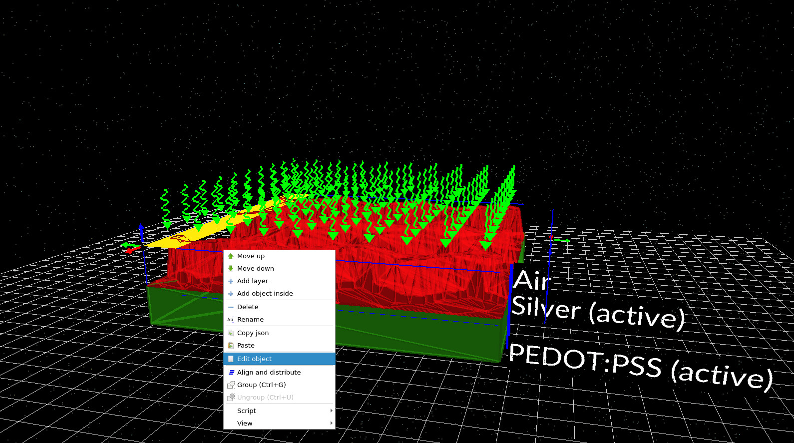
This editor makes almost every aspect of the object editable. However, note that this mesh sits inside a layered epitaxial structure rather than free space, so some options are naturally constrained by the surrounding layer stack.
- Attributes: change the colour (and alpha) to make the object easier to see in the view.
- Optical material: replace the material definition (useful if electrical and optical simulations are combined).
- Object shape: select the geometric pattern used to construct the mesh (this is the most important control for electrical performance).
Step 2: Change the honeycomb pattern via the Mesh Editor
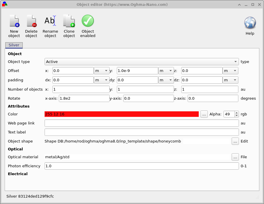
In the Object Editor, locate the Object shape option. At present, the mesh is called from the Shape Database (for example honeycomb). Click the three dots next to Edit to open the Mesh Editor (see ??).
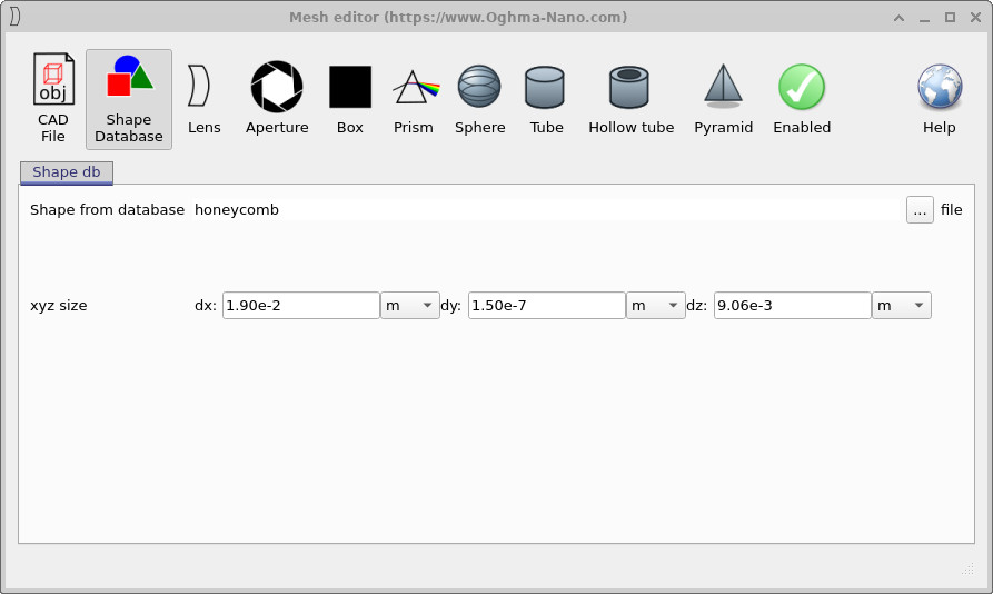
In the Mesh Editor, click the three dots to the right of Shape from database. This opens the Shape Database browser (see ??). In this example, we navigate to a folder containing several types of honeycomb pattern (previously used for figures in a paper) and select one of them.
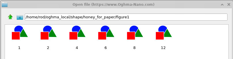
Not all shapes are physically meaningful for contacts. A contact mesh should form a continuous conducting network that makes sensible contact with the underlying polymer. Decorative or free-form shapes (for example gaussian or teapot) usually do not create a valid current-collection structure. Honeycomb patterns are a natural starting point because they create a connected network with repeating cells.
If you want to create your own patterns (for example from a printed mask image), follow the process described in /manual/tutorial-shape-db-part-a.html and then import them into the Shape Database.
Step 3: Change the device size
You can change the overall device size by clicking Substrate xz-size in the left-hand side of the main window. This opens the dimension editor shown in ??.
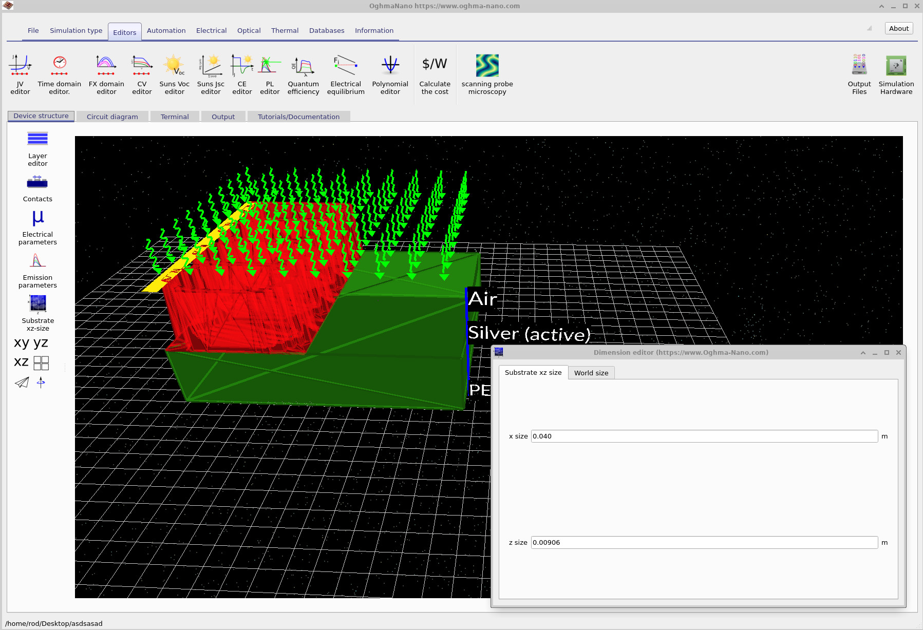
In the example above, the substrate size has been doubled. You will immediately notice an important point: the substrate becomes larger, but the honeycomb mesh does not automatically follow it. This is because the mesh is a 3D object whose absolute dimensions are defined in the Mesh Editor (see ??), not by the substrate size control.
Changing the device size is therefore a two-step operation:
- Change the size of the substrate (the world/device size).
- Change the size of the mesh object in the Mesh Editor so that it covers the full new substrate.
Conclusion: A general workflow for complex 3D contact problems
You have now seen a complete workflow for simulating large-area transparent/metal contacts:
- Build a layered contact stack (polymer + metal mesh + extraction contact).
- Run the scan solver to map effective resistance and voltage drop across the device.
- Change the geometry (mesh pattern, size, pitch) and rerun to quantify the improvements.
This method is not limited to solar cells. Any device in which current must spread laterally through a resistive layer—OLED panels, electrochromic materials, sensors, flexible electronics, large-area photodetectors—can be analysed in the same way. The key point is that the physics of the problem is dominated by resistive current collection, and so a 3D circuit representation is both appropriate and computationally efficient.
👉 Next step: Apply this workflow to your own contact patterns by importing shapes into the Shape Database and adjusting the resistances to match your measured materials.