شبیهسازی دستگاه با مساحت بزرگ – بخش C: ویرایش هندسه تماس (شکل و اندازه)
در بخش B هندسه تماس را ثابت در نظر گرفتیم و بررسی کردیم که چگونه تلفات مقاومتی به خواص مواد و تنظیمات اسکن وابسته است. با این حال، در عمل قدرتمندترین پارامتر قابل تنظیم شما هندسه است: الگوی مش، گام آن، عرض خطوط، و اندازه دستگاهی که باید پوشش دهد.
در این بخش ساختار فیزیکی تماس را تغییر میدهیم. این شامل جابجایی بین الگوهای مختلف لانهزنبوری، ویرایش ابعاد مش پایه، و تغییر اندازه زیرلایه شبیهسازیشده است.
💡 نکته: اگر میخواهید الگوهای مش خود را از تصاویر دوبعدی (برای مثال از یک ماسک چاپی، تصویر میکروسکوپی، یا خروجی CAD) تولید کنید، به /manual/tutorial-shape-db-part-a.html مراجعه کنید. این همان روند کاری است که برای پر کردن Shape Database مورد اشاره در ادامه استفاده میشود.
گام ۱: باز کردن Object Editor برای مش فلزی
در نمای سهبعدی، روی مش فلزی ششضلعی راستکلیک کرده و گزینه Edit object را انتخاب کنید (نگاه کنید به ??). این کار Object Editor را باز میکند (??).
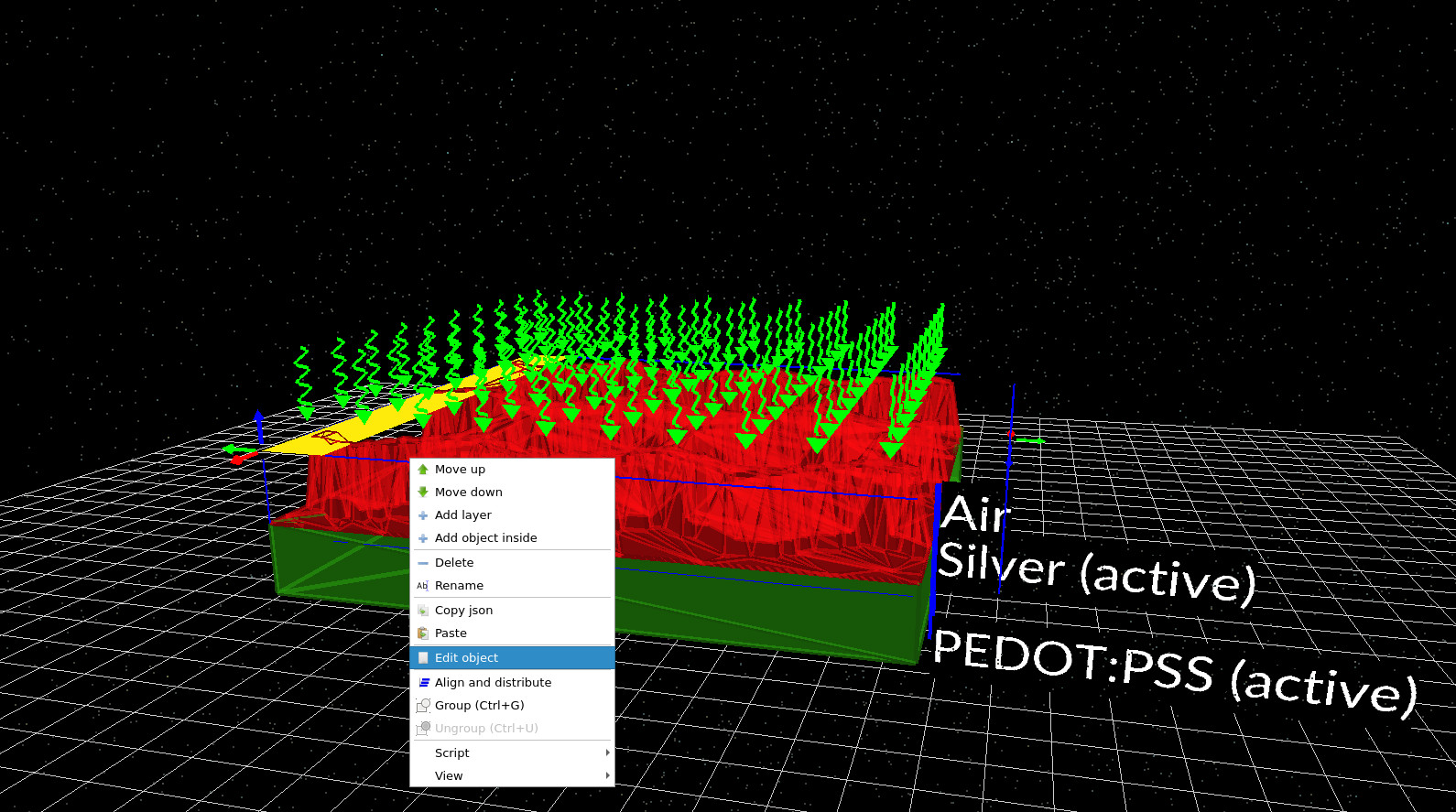
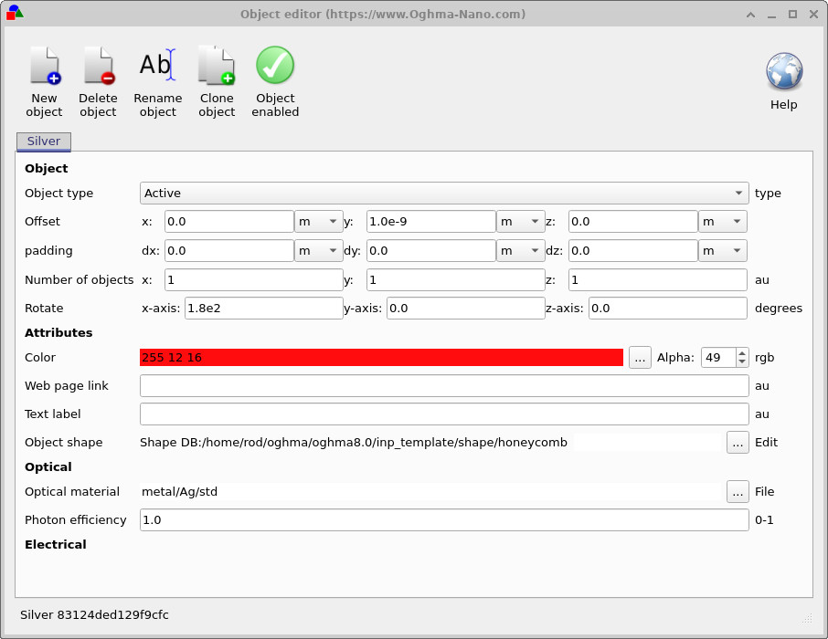
این ویرایشگر به شما اجازه میدهد تقریباً تمام جنبههای شیء را تغییر دهید. با این حال توجه داشته باشید که این مش درون یک ساختار اپیتاکسی لایهای قرار دارد و در فضای آزاد نیست، بنابراین برخی گزینهها به طور طبیعی توسط پشته لایهها محدود میشوند.
- Attributes: تغییر رنگ (و آلفا) برای وضوح بیشتر در زمان تجسم.
- Optical material: جایگزینی تعریف ماده (در صورتی که بعداً کارهای الکتریکی + نوری را ترکیب کنید مفید است).
- Object shape: انتخاب الگوی هندسی مورد استفاده برای ساخت مش (این مهمترین کنترل برای عملکرد الکتریکی است).
گام ۲: تغییر الگوی لانهزنبوری از طریق Mesh Editor
در Object Editor، گزینه Object shape را پیدا کنید. مش در حال حاضر از Shape Database (مثلاً honeycomb) گرفته شده است. روی سه نقطه کنار Edit کلیک کنید تا Mesh Editor باز شود (نگاه کنید به ??).
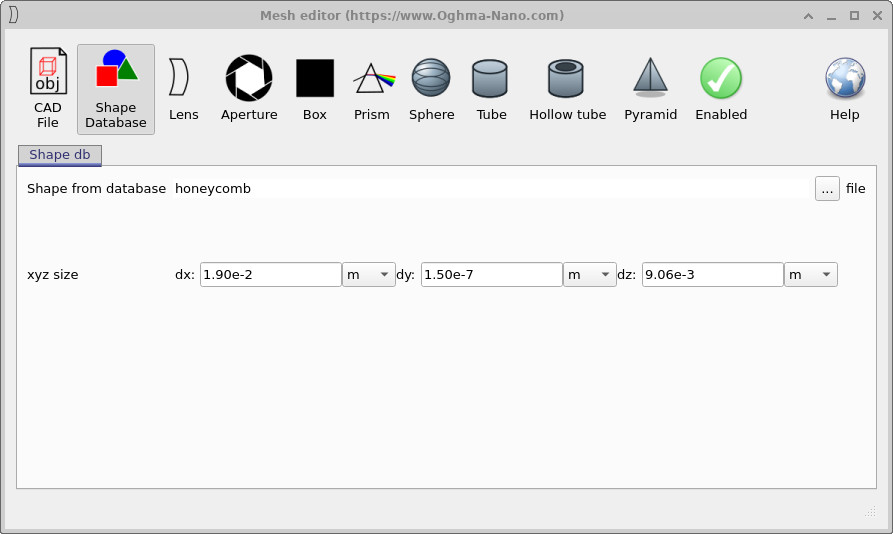
در Mesh Editor، روی سه نقطه سمت راست Shape from database کلیک کنید. این کار مرورگر Shape Database را باز میکند (نگاه کنید به ??). در این مثال، به پوشهای شامل چندین نوع لانهزنبوری (که قبلاً برای شکلهای مقاله استفاده شدهاند) میرویم و یکی را انتخاب میکنیم.
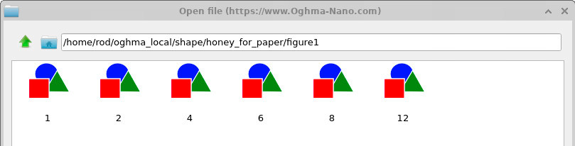
همه شکلها برای تماسها از نظر فیزیکی معنیدار نیستند. یک مش تماس باید یک شبکه رسانای پیوسته تشکیل دهد که بهطور منطقی با پلیمر زیر آن تماس داشته باشد. شکلهای تزئینی یا آزاد (برای مثال گاوسیها یا قوریها) معمولاً ساختار جمعآوری جریان معتبری تشکیل نمیدهند. الگوهای نوع لانهزنبوری نقطه شروع طبیعی هستند زیرا یک مش پیوسته با سلولهای تکرارشونده ایجاد میکنند.
اگر میخواهید الگوهای خود را ایجاد کنید (برای مثال از تصویر یک ماسک چاپی)، روند کاری در /manual/tutorial-shape-db-part-a.html را دنبال کرده و سپس آنها را در Shape Database وارد کنید.
گام ۳: تغییر اندازه دستگاه
میتوانید اندازه کلی دستگاه را با کلیک روی Substrate xz-size در نوار سمت چپ پنجره اصلی تغییر دهید. این کار ویرایشگر ابعاد نشان دادهشده در ?? را باز میکند.
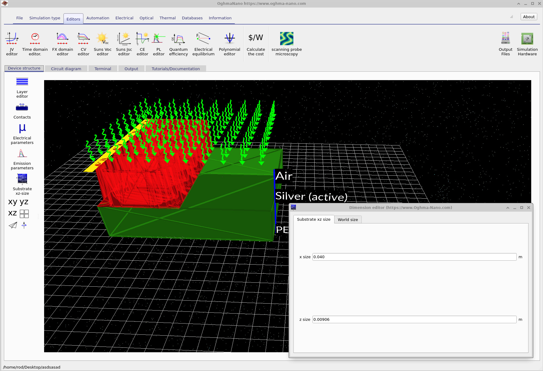
در مثال بالا اندازه زیرلایه دو برابر شده است. فوراً نکته مهمی را مشاهده میکنید: زیرلایه رشد میکند، اما مش لانهزنبوری بهطور خودکار دنبال آن تغییر نمیکند. این به این دلیل است که مش یک شیء سهبعدی است که ابعاد مطلق آن در Mesh Editor تنظیم میشود (نگاه کنید به ??) و نه توسط کنترل اندازه زیرلایه.
بنابراین تغییر اندازه دستگاه یک عملیات دو مرحلهای است:
- تغییر اندازه substrate (اندازه جهان/دستگاه).
- تغییر اندازه mesh object در Mesh Editor بهگونهای که کل زیرلایه جدید را پوشش دهد.
جمعبندی: یک روند کاری عمومی برای مسائل پیچیده تماس سهبعدی
اکنون یک روند کاری کامل برای شبیهسازی تماسهای شفاف/فلزی با مساحت بزرگ را مشاهده کردهاید:
- ساخت یک پشته تماس لایهای (پلیمر + مش فلزی + تماس استخراج).
- اجرای حل اسکن برای نقشهبرداری مقاومت مؤثر و افت ولتاژ در سراسر دستگاه.
- تغییر هندسه (الگوی مش، اندازه، گام) و اجرای مجدد برای کمیسازی بهبودها.
این روش محدود به سلولهای خورشیدی نیست. هر دستگاهی که در آن جریان باید به صورت جانبی از طریق یک لایه مقاومتی پخش شود—پنلهای OLED، دستگاههای الکتروکرومیک، حسگرها، الکترونیک انعطافپذیر، فوتودتکتورهای با مساحت بزرگ—میتواند به همین روش بررسی شود. نکته کلیدی این است که فیزیک توسط جمعآوری جریان مقاومتی غالب میشود و بنابراین یک نمایش مدار سهبعدی هم مناسب و هم از نظر محاسباتی کارآمد است.
👉 گام بعدی: این روند کاری را برای الگوهای تماس خود با وارد کردن شکلها در Shape Database و تنظیم مقاومت ویژهها مطابق با مواد اندازهگیریشده خود به کار ببرید.