The need for trap states in organic device models
This section explains why trap states must be considered when simulating disordered materials such as polymer:fullerene blends, small-molecule systems, or amorphous semiconductors. Without an explicit treatment of trapping and release, any device model will fail to capture the physics of charge transport and recombination. Using the full Shockley–Read–Hall (SRH) recombination and trapping formalism is therefore essential for obtaining physically meaningful results.
Key take home message, Why trap states must be included:
- If you ignore trap states, the Fermi level–electron density relation will be wrong.
- An incorrect Fermi-level dependence means recombination vs. voltage will also be wrong.
- Mobility vs. voltage will likewise be misrepresented.
- As a result, you cannot reproduce realistic J–V curves with physically meaningful parameters.
Key takeaway: Ensuring the correct carrier–Fermi level dependence is critical; without it, device simulations will fail to capture real physical behaviour.
1. The physical and energetic structure of disordered materials
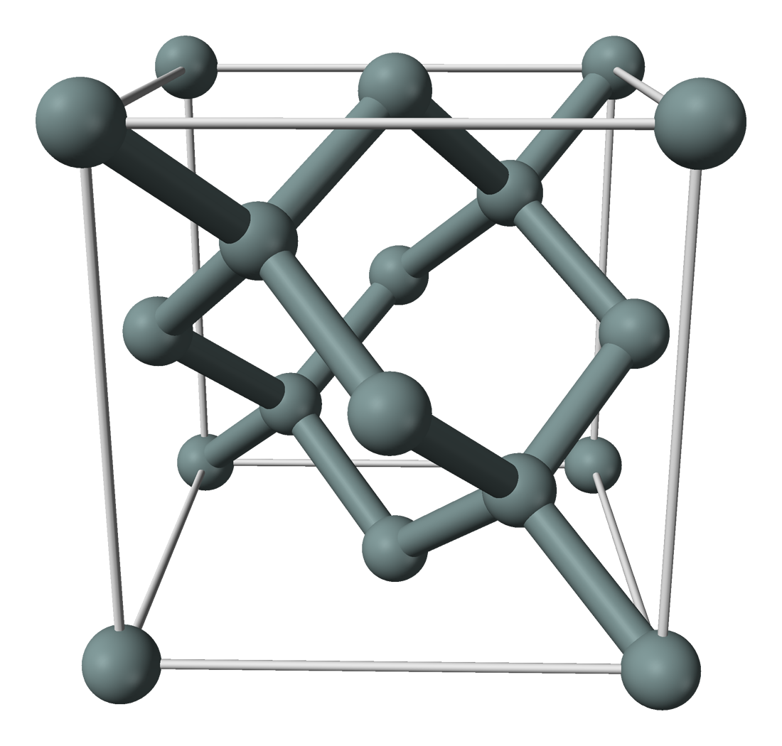
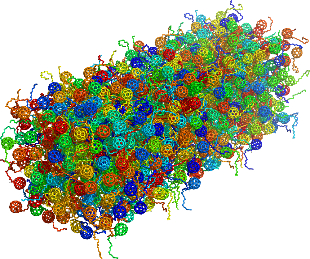
Traditional inorganic semiconductors such as crystalline Si or GaAs are both highly ordered and extremely pure — often achieving “nine-nines” purity (99.9999999%). Organic semiconductors, by contrast, rarely exceed 99.9% purity, making them around a million times more defect-rich than their inorganic counterparts. Structurally, the difference is equally stark: inorganic semiconductors form regular crystalline lattices, like marbles neatly packed on a solitaire board (??). Silicon itself adopts the diamond cubic structure, a nearly perfect lattice (??). Organic materials, in contrast, are “floppy” molecular systems, with tangled polymers resembling a plate of spaghetti bolognese — the spaghetti representing polymer chains and the sauce the small molecules (??). Simulations of organic blends confirm this picture, showing spaghetti-like polymer packing with fullerene derivatives interspersed throughout (??).


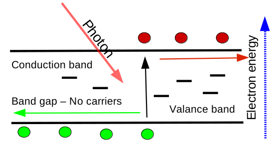
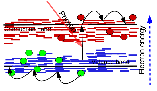
These structural differences give rise to very different energetic landscapes. In crystalline semiconductors, electrons and holes move freely in well-defined conduction and valence bands, experiencing only modest resistance under an applied field. This band-like transport is illustrated in ??. In disordered organic semiconductors, however, impurities and structural disorder introduce a dense distribution of localized trap states within the band gap. Instead of propagating freely through extended states, carriers must thermally hop between traps. This trap-dominated transport is shown schematically in ??.
The implication is clear: while trap states can often be neglected in ordered semiconductors, they dominate the physics of disordered systems. Any realistic device model must therefore include a detailed description of trap distributions and Shockley–Read–Hall kinetics. OghmaNano does exactly this, making it possible to simulate disordered systems such as organic solar cells, OFETs, and perovskites with physical accuracy.
To see why this matters, we now turn to the relationship between carrier density and the Fermi level, to examine some concrete examples.
Key takeaways:
- Ordered semiconductors (e.g. Si, GaAs) are extremely pure and crystalline, so carriers move freely in band-like states.
- Disordered semiconductors (e.g. organics, perovskites) are impurity-rich and structurally messy, so transport is dominated by trap states and hopping.
2. Why trap states are important for device modelling (no maths)
A central feature of organic and other disordered semiconductors is that the carrier density is a strong function of both applied voltage and illumination intensity. As bias or light intensity increases, more charge is injected or photogenerated into the device. Because these materials possess a large number of trap states within the band gap, carriers first fill these traps before occupying extended states. This trap filling means that even small changes in voltage can produce large changes in the free-carrier density.
This matters because recombination in the device depends directly on carrier densities. The general form of the recombination rate is
\[ R = k_r \, n(V)\, p(V), \]
where \(k_r\) is the recombination constant, and \(n(V)\) and \(p(V)\) are the voltage-dependent electron and hole densities. If the functional form of \(n(V)\) (and \(p(V)\)) is wrong because trap states have been neglected, then the recombination rate will also be wrong. This leads directly to incorrect predictions of open-circuit voltage (\(V_{OC}\)) and other key device characteristics.
Mobility is similarly affected. In disordered systems, the effective carrier mobility depends on the balance between free carriers and trapped carriers. A simple expression is
\[ \mu_e(n) = \frac{\mu_e^0 \, n_{\text{free}}}{n_{\text{free}} + n_{\text{trap}}}, \]
where \(\mu_e^0\) is the intrinsic electron mobility, \(n_{\text{free}}\) is the density of mobile carriers, and \(n_{\text{trap}}\) is the density of trapped carriers. If the density–voltage relationship is wrong, then the predicted mobility–voltage dependence will also be wrong. Together, these errors mean the simulated J–V curve will not match experiment, even if recombination or mobility parameters are otherwise reasonable.
Key takeaways:
- If trap states are ignored, the carrier density vs. voltage relationship is wrong, leading to incorrect recombination rates and \(V_{OC}\).
- Effective mobility depends on the balance of free vs. trapped carriers, so neglecting traps also gives the wrong mobility–voltage dependence and J–V curves.
3. Why trap states are important for device modelling (with maths)
To describe carrier densities correctly, one must account for the underlying density of states (DoS). Figure ?? sketches the DoS corresponding to the ordered and disordered band structures shown earlier in ?? and ??. In an ordered semiconductor, the DoS has a sharp band edge (parabolic band), and the Fermi–Dirac population lies above the conduction-band edge. In a disordered semiconductor, however, the DoS exhibits a tail of localized trap states that extends deep into the band gap (commonly modeled with exponential or Gaussian tails). The consequence is that carriers occupy fundamentally different distributions in the two cases.
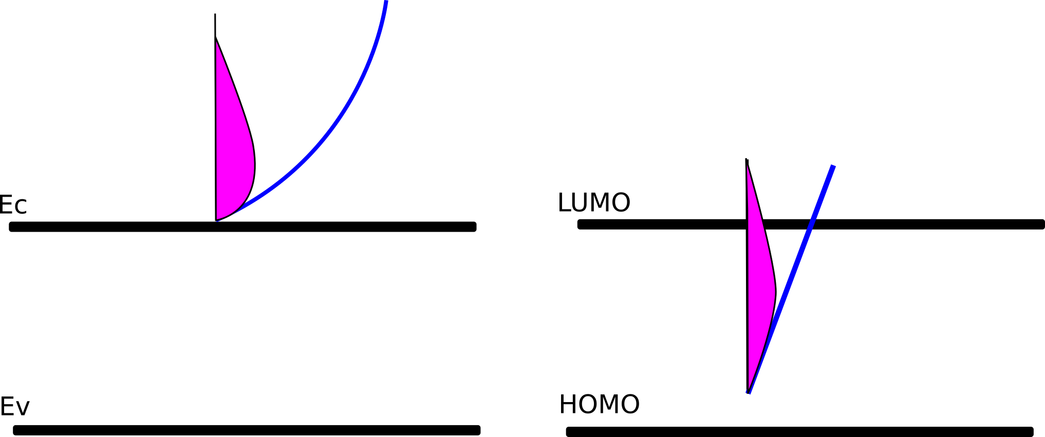
Formally, the total electron density is given by integrating the DoS weighted by the Fermi–Dirac occupation:
\[ n(E_f,T) = \int_{E_{\min}}^{\infty} \rho(E)\, f(E,E_f,T)\, dE, \]
where \(E_f\) is the quasi-Fermi level, \(\rho(E)\) is the DoS, and \(f(E,E_f,T)\) is the Fermi–Dirac distribution. In ordered materials, \(\rho(E)\) is sharp, so only states above the conduction-band edge contribute. In disordered materials, \(\rho(E)\) includes extensive trap tails, so carriers can be stored close to the Fermi level, producing charge densities one to two orders of magnitude larger than in an ordered crystal at the same bias. This is directly observed in charge-extraction experiments.
The conclusion is straightforward: getting the carrier density dependence correct is not optional. Without a trap-state model, both recombination and mobility will be wrong as functions of voltage, and realistic J–V curves cannot be reproduced. OghmaNano includes these trap states explicitly, enabling accurate modeling of disordered devices such as PM6:Y6 and P3HT:PCBM blends, as well as more ordered semiconductors when traps are disabled.
Key takeaways:
- In ordered semiconductors, carriers mainly occupy extended states above sharp band edges.
- In disordered semiconductors, trap-tail states dominate, storing carriers deep in the band gap.
- Without including trap states in the DoS, carrier density vs. voltage is wrong, leading to incorrect recombination, mobility, and J–V curves.
4. Why you should not use Langevin recombination in device models
The classical Langevin recombination rate is defined as
\[ R_{\text{free}} = q \, k_r \, \frac{\mu_e + \mu_h}{2 \, \epsilon_0 \epsilon_r} \, n p , \]
where \(R_{\text{free}}\) is the recombination rate, \(k_r\) is the empirical Langevin reduction factor, \(\mu_e\) and \(\mu_h\) are the electron and hole mobilities, \(n\) and \(p\) are the carrier densities, and \(\epsilon_0 \epsilon_r\) is the dielectric permittivity. At first glance this seems physically reasonable: recombination is assumed to occur whenever an electron and a hole approach closely enough under Brownian motion to feel each other’s Coulomb field. This picture is appropriate for perfectly free carriers in simple liquids or ionic conductors. But in organic photovoltaic (OPV) and other disordered semiconductors, the assumptions behind the Langevin model break down.
Why does it fail? Experimental studies — especially from the early 2010s — quickly showed that Langevin recombination could not self-consistently reproduce both dark and illuminated J–V curves. The model systematically overestimated recombination rates, often by orders of magnitude. To make fits possible, researchers introduced a “Langevin reduction factor” \(k_r\), sometimes as small as 10−3. While convenient, this adjustment was really an admission that the mechanism itself was not valid in these systems.
The problems are clear when we look more closely at the equation:
- Wrong carrier-density dependence. The rate scales strictly as \(np\), i.e. second order. In experiments, recombination in OPVs often follows non-integer power laws such as \((np)^{1.5}\), reflecting trap-limited dynamics and the distribution of localized states. The Langevin form simply cannot capture this.
- Incorrect treatment of mobility. The equation assumes fixed mobilities \(\mu_e\) and \(\mu_h\). In reality, mobility in disordered semiconductors is strongly carrier-density dependent (see discussion above). Folding in the wrong mobility dependence further distorts the predicted recombination rate.
- Ignores traps and disorder. The Langevin mechanism treats all carriers as free. In OPVs and similar materials, most carriers spend time trapped in localized states and only intermittently contribute to conduction. Recombination therefore depends on the trap landscape, not just free-carrier motion.
Taken together, these issues mean Langevin recombination is at best a crude approximation and at worst a misleading one. Even with a fitted reduction factor \(k_r\), it fails to capture the correct physics of trap-assisted recombination and the voltage dependence of mobility. Using Langevin recombination in device models is therefore like forcing a square peg into a round hole: it may give you a number, but it will not give you physically meaningful results.
Key takeaways on Langevin recombination
- Langevin recombination systematically overestimates rates in OPVs and disordered semiconductors.
- It assumes all carriers are free, with fixed mobilities — ignoring traps and carrier-density dependence.
- Reduction factors (\(k_r\)) were historically introduced to force fits, but this highlights the model’s invalidity.
- Accurate modelling requires trap-assisted recombination mechanisms (e.g. Shockley–Read–Hall), not Langevin.
5. How one can make Langevin recombination “work” in device models
The key problems with classical Langevin recombination are its incorrect dependence on carrier density and the need for an arbitrary reduction factor. One way researchers have attempted to make Langevin recombination “work” is by introducing a carrier-density dependence into the mobilities themselves, as in:
\[ R_{\text{free}} = q \, k_r \, \frac{\alpha \mu_e(n) + \beta \mu_h(n)}{2 \, \epsilon_0 \epsilon_r} \, n_{\text{tot}} p_{\text{tot}} , \]
Here, a mobility edge is defined: carriers above the mobility edge contribute to conduction, while those below are considered trapped. The average mobilities can then be expressed as
\[ \mu_e(n) = \frac{\mu_e^0 \, n_{\text{free}}}{n_{\text{free}} + n_{\text{trap}}}, \qquad \mu_h(p) = \frac{\mu_h^0 \, p_{\text{free}}}{p_{\text{free}} + p_{\text{trap}}}. \]
If the density of free carriers is much smaller than the density of trapped carriers, this leads to an effective recombination rate of
\[ R(n,p) = q \, k_r \, \frac{\alpha \mu_e^0 \, n_{\text{free}} p_{\text{trap}} + \beta \mu_h^0 \, p_{\text{free}} n_{\text{trap}}} {2 \, \epsilon_0 \epsilon_r}. \]
In this way, Langevin recombination is effectively reinterpreted in terms of interactions between free and trapped carriers (\(n_{\text{free}}p_{\text{trap}}\) and \(p_{\text{free}}n_{\text{trap}}\)). This is, in essence, equivalent to the Shockley–Read–Hall (SRH) picture of recombination: free carriers recombining with trapped carriers.
While this approach works reasonably well in steady state, it relies on a strong assumption: that all carriers at a given position share a single quasi-Fermi level, i.e. they are in local equilibrium with infinite thermalization velocity. This may be plausible under steady-state conditions, when carriers have time to equilibrate, but it breaks down in the time domain. In reality, the dense distribution of trap states in organic semiconductors makes it unlikely that carriers can act as a single equilibrated gas. By contrast, the SRH formalism avoids this assumption, and is therefore a more physically sound description of recombination and trapping in disordered materials.
Overall takeaways:
- Trap states dominate charge transport and recombination in disordered semiconductors.
- Accurate carrier density vs. voltage dependence is essential for realistic modeling.
- Incorrect treatment of traps leads to wrong recombination, mobility, and JV curves.
- OghmaNano includes a full trap-state and SRH treatment, enabling meaningful device simulations.