

Shockley–Read–Hall (SRH) Recombination Model
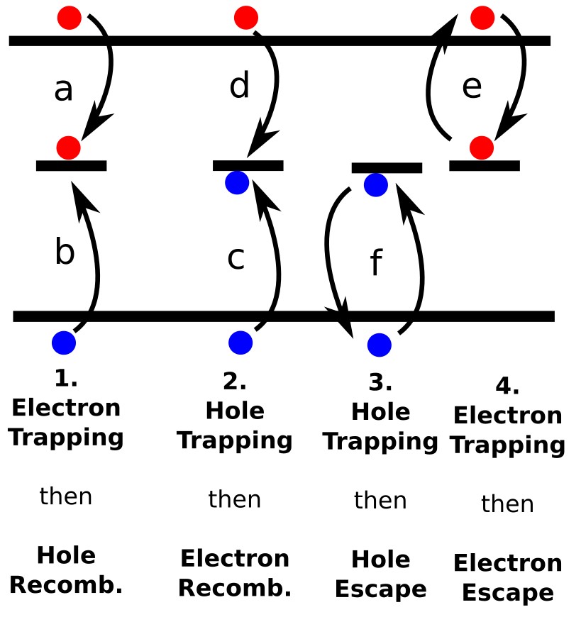
(2) Hole trapping (d) followed by electron recombination (c).
(3) Hole trapping (f) with subsequent thermal hole escape.
(4) Electron trapping (e) with subsequent thermal electron escape.
SRH recombination is a non-radiative recombination process in semiconductors where electrons and holes recombine via defect (trap) states within the band gap.
Shockley–Read–Hall (SRH) recombination is a non-radiative, trap-assisted recombination process in semiconductors in which electrons and holes recombine via localized defect states within the band gap. It proceeds in two stages: a carrier is first captured into a trap, and then may either recombine with an opposite carrier or re-emerge by thermal excitation. ?? illustrates the four main pathways for a single mid-gap trap state, with transitions labelled (a–f).
- 1. Electron trapping: capture of an electron (a), followed by recombination with a trapped hole (b).
- 2. Hole trapping: capture of a hole (d), followed by recombination with a trapped electron (c).
- 3. Hole trapping with escape: capture of a hole, followed by thermal re-emission (f).
- 4. Electron trapping with escape: capture of an electron, followed by thermal re-emission (e).
These processes show that the same trap can mediate both recombination and carrier release. SRH recombination is inherently a two-stage mechanism: first, a carrier is captured (a, d), and only later does recombination occur when the opposite carrier is captured (b, c). If no opposite carrier arrives, the trapped carrier may thermally escape (e, f). The overall efficiency of SRH recombination depends on trap density, energy level within the band gap, carrier capture cross-sections, and the relative lifetimes of trapped carriers.
Standard SRH Recombination Rate
The net trap-assisted recombination rate under the steady-state Shockley–Read–Hall (SRH) model is given by
\[ R_{\mathrm{SRH}} = \frac{np - n_{\mathrm{eq}} p_{\mathrm{eq}}} {\tau_{p}(n + n_{1}) + \tau_{n}(p + p_{1})} \]
where \(n\) and \(p\) are the local electron and hole densities, and \(n_{\mathrm{eq}}\) and \(p_{\mathrm{eq}}\) denote their equilibrium values. Writing the numerator in this form ensures that the net recombination rate vanishes exactly at equilibrium.
The effective electron and hole lifetimes associated with the trap are
\[ \tau_n = \frac{1}{\sigma_n v_{\mathrm{th}} N_t}, \qquad \tau_p = \frac{1}{\sigma_p v_{\mathrm{th}} N_t}, \]
where \(N_t\) is the trap density, \(\sigma_n\) and \(\sigma_p\) are the electron and hole capture cross-sections, and \(v_{\mathrm{th}}\) is the thermal velocity.
The auxiliary SRH quantities \(n_1\) and \(p_1\) represent the carrier densities for which the trap is in equilibrium with the conduction and valence bands, respectively. They are defined as
\[ n_1 = n_i \exp\!\left(\frac{E_t - E_{\mathrm{ref}}}{k_B T}\right), \qquad p_1 = n_i \exp\!\left(\frac{E_{\mathrm{ref}} - E_t}{k_B T}\right), \]
where \(E_t\) is the trap energy level and \(E_{\mathrm{ref}} = E_g/2\) is the mid-gap reference energy. The intrinsic carrier concentration \(n_i\) is defined through the equilibrium condition
\[ n_i^2 = n_{\mathrm{eq}} p_{\mathrm{eq}}. \]
A trap energy \(E_t = E_{\mathrm{ref}}\) therefore corresponds to a mid-gap defect, while positive or negative values shift the trap towards the conduction or valence band, respectively.
In this formulation, recombination is mediated by a single defect level that can capture both electrons and holes. Despite its simplicity, the SRH model captures the dominant role of defect-assisted recombination in many semiconductor devices and provides a computationally efficient description suitable for steady-state device simulations. See the derivation of the Shockley–Read–Hall (SRH) recombination equation.
Try SRH recombination in these device simulations
Run the GaAs PN junction diode tutorial to see how SRH recombination appears alongside radiative recombination in a high-quality semiconductor, and compare it with the silicon PN junction diode tutorial, where SRH recombination controls dark I–V behaviour and depletion-region losses. For organic devices, use the organic solar-cell recombination tutorial, where SRH traps are compared directly with bimolecular recombination.
Limitations of the Standard SRH Model
While powerful, the standard SRH equation comes with several important limitations:
- Single-level approximation — it accounts for only one discrete trap energy, whereas real semiconductors (particularly organics and disordered systems) typically contain a broad distribution of trap states.
- No explicit electrostatics — the model treats traps as purely recombination centers. Charges temporarily captured in traps are not included in the electrostatic potential of the device, so their effect on space charge and internal fields is ignored.
- Purely recombination-focused — the expression does not describe trapping and de-trapping dynamics explicitly, only their net effect as recombination.
To overcome these limitations, one must explicitly solve the SRH formalism across a distribution of trap states, allowing both the recombination rate and the trap occupation (and thus their electrostatic contribution) to be correctly represented. This more general treatment is described here.
In OghmaNano, the standard SRH recombination term can be enabled or disabled in the Electrical parameter editor, and the lifetimes \(\tau_{n}\) and \(\tau_{p}\) can be specified by the user.
From single-level SRH recombination to distributed trap states
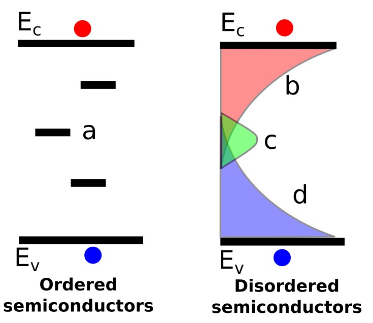
The standard SRH equation assumes recombination occurs through a single discrete trap level. This approximation is often reasonable for relatively ordered semiconductors such as crystalline silicon or GaAs, where trap states can frequently be treated as isolated defects within the band gap. However, as illustrated in ??, disordered semiconductors such as amorphous silicon and organic semiconductors typically contain broad distributions of localized states extending through the band gap rather than a small number of isolated point defects.
In these systems, the trap distribution influences not only recombination but also charge storage, quasi-Fermi-level position, electrostatic band bending and carrier transport. As discussed in why trap states are needed in disordered semiconductor models, the occupation of localized states can strongly modify carrier densities, effective mobility, recombination rates and the shape of the device J–V curve. Under these conditions, it becomes more useful to treat SRH recombination as a distributed trapping and detrapping process occurring across an entire density of states rather than through one discrete mid-gap defect.
The distributed trap-state modelling tutorial demonstrates how these effects appear in practice using a PM6:Y6 organic solar-cell simulation as a worked example. However, the same physical ideas apply more broadly to many disordered semiconductor systems including amorphous silicon, perovskites, oxide semiconductors and other thin-film electronic and photovoltaic materials where localized states strongly influence transport and recombination.
Where to go next
Continue to Shockley–Read–Hall (SRH) trapping and recombination (non-equilibrium), where the model is extended to include trap distributions, electrostatic coupling, and time-dependent behaviour. To see how SRH recombination limits real devices, explore the silicon PN junction diode tutorial (dark I–V and lifetime sweeps), the amorphous silicon solar-cell tutorial (defect-dominated recombination and voltage loss), and the organic solar-cell recombination tutorial, where SRH is compared with bimolecular recombination.
🎯 This progression takes you from the analytical SRH model to dynamic trap physics and finally to real device simulations.