Semiconductor Interface Models in OghmaNano: Drift–Diffusion, Tunnelling, and Charge Doping
1. Introduction to interfaces
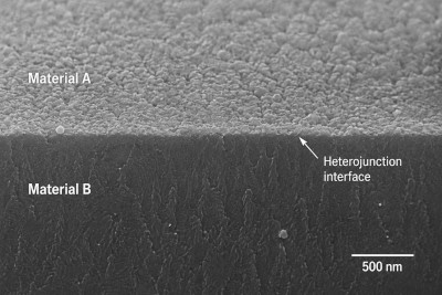
Interfaces play a central role in semiconductor device physics because they determine how charge carriers move through a device. By engineering energetic offsets between materials, interfaces can confine electrons and holes, block unwanted carrier flow, or selectively assist charge extraction. Nearly all modern semiconductor devices rely on interfaces to control transport, including heterojunction solar cells, OLEDs, OFETs, tunnel junctions, perovskite devices, and quantum-well structures.
Within a drift–diffusion simulation, interfaces are represented through discontinuities in material parameters such as the electron affinity, band gap, density of states, mobility, or permittivity. These discontinuities produce offsets in the conduction and valence bands which modify the local carrier transport. Depending on the energetic alignment, an interface may either assist carrier transfer or suppress current flow.
In OghmaNano, the simplest interface treatment is to apply no additional interface transport model at all and allow the standard drift–diffusion equations to determine the carrier transport naturally from the local band structure and quasi-Fermi level gradients. Additional models, such as tunnelling or hopping, can then be added on top of this baseline description when extra transport mechanisms are required.
2. Drift–diffusion over interfaces
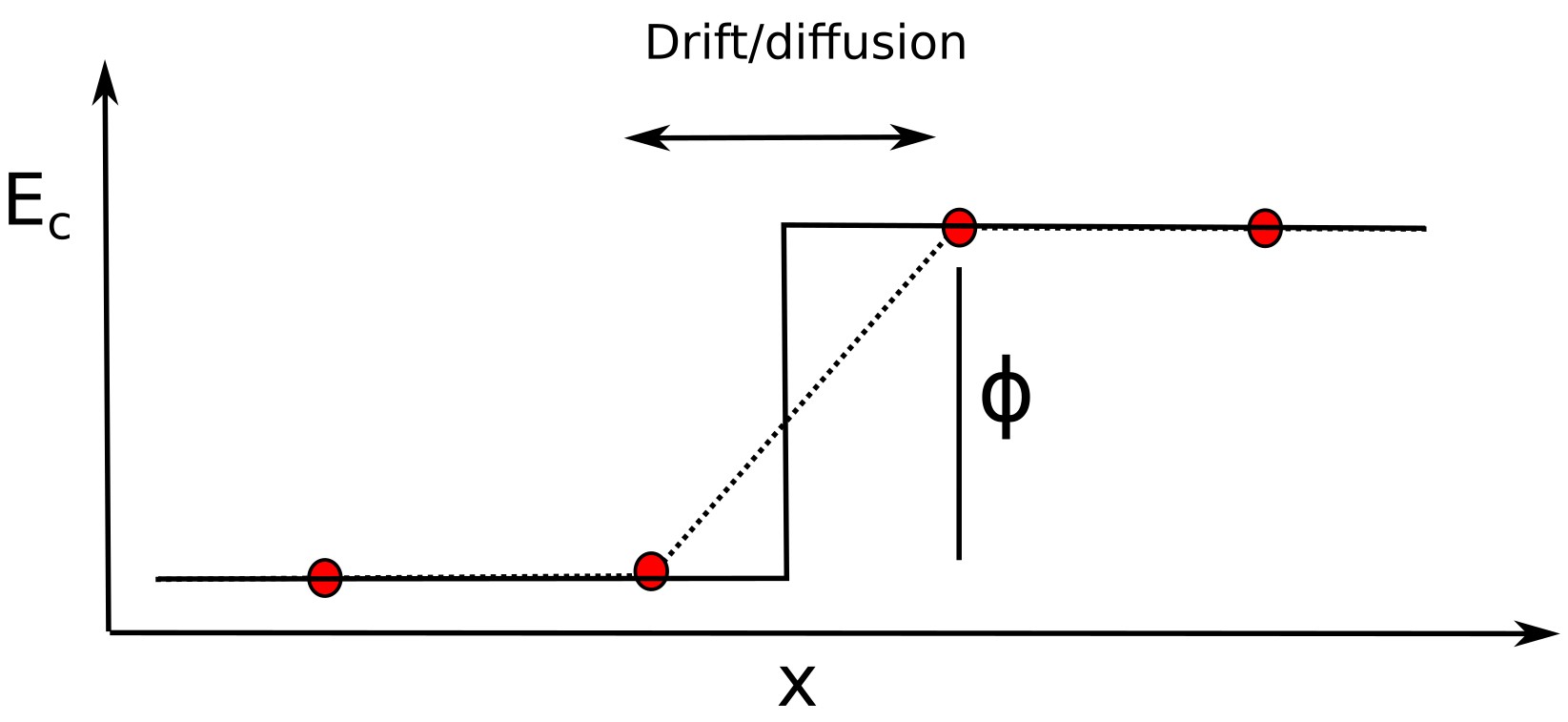
The simplest interface model is to allow charge carriers to drift and diffuse directly across a heterojunction according to the local electrostatic potential and carrier density gradients. In this case, no explicit tunnelling or hopping current is added at the interface. Instead, the drift–diffusion equations determine the carrier transport self-consistently from the local band structure.
An example of this is shown in ??. Here the conduction band contains an abrupt energetic step of height \(\phi\). Electrons approaching the interface must overcome this barrier through ordinary drift and diffusion transport. As the energetic offset increases, the carrier density above the barrier decreases exponentially, naturally suppressing the current flow across the interface.
The numerical representation of the heterojunction strongly depends on the spatial mesh resolution. If the interface is represented using a very fine mesh, the energetic step becomes steeper and the resulting electric field at the interface increases significantly. Under these conditions, the drift–diffusion equations may predict very strong carrier blocking behaviour. Conversely, if the interface is represented using fewer mesh points, the energetic transition becomes smoother, reducing the local gradient and allowing carriers to diffuse more easily across the junction.
In practice, this means that interfaces often require relatively fine meshing if their full blocking behaviour is to be captured accurately. This is particularly important for sharply varying heterojunctions, thin transport layers, and strongly confined electronic structures.
By default, carriers in OghmaNano already drift and diffuse across interfaces according to the gradients of the conduction and valence bands. Uphill band offsets suppress carrier flow, while downhill alignments allow easy carrier transfer. The additional interface models described below sit on top of this baseline drift–diffusion picture, providing extra transport channels that can assist carriers in overcoming energetic barriers.
3. Direct tunnelling
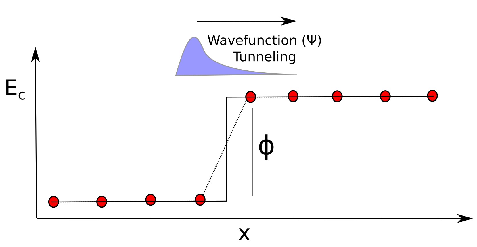
For sufficiently thin interfaces, quantum-mechanical tunnelling can provide an additional transport pathway across an energetic barrier. Rather than requiring carriers to thermally overcome the full band offset, the carrier wavefunction can penetrate through the classically forbidden region, leading to a finite probability of transmission across the interface.
An example of this process is shown in ??. Here the conduction band contains a heterojunction energy step of height \(\phi\). The shaded region above the barrier represents the exponentially decaying carrier wavefunction inside the forbidden region. Although the carrier energy lies below the barrier height, the wavefunction remains finite across the interface, allowing a small tunnelling current to flow.
The tunnelling current density can be approximated using a WKB expression of the form:
\[ \boldsymbol{J} = A(n-n^{eq})V \exp\left( -\frac{2d}{\hbar}\sqrt{2mq\phi} \right) \]
Here, \(A\) is a prefactor containing material and geometrical constants, \(V\) is the applied bias, \(\phi\) is the barrier height, \(m\) is the carrier effective mass, \(d\) is the effective barrier thickness, \(q\) is the elementary charge, and \(\hbar\) is the reduced Planck constant. The exponential dependence originates from the decay of the carrier wavefunction inside the forbidden region. Thicker barriers or larger energetic offsets therefore suppress the tunnelling current exponentially.
In OghmaNano this expression is implemented in a simplified form:
\[ \boldsymbol{J} = A(n-n^{eq})V \exp\left( -B\sqrt{\phi} \right) \]
Here the parameter \(B\) absorbs the barrier thickness, effective mass, and other physical constants into a single fitting parameter. This simplified form captures the dominant exponential dependence of the tunnelling current on the barrier height while remaining numerically efficient. The parameters associated with this model can be configured using the interface editor.
4. Interface-assisted transport (organic–organic)
At organic heterojunctions, carrier transfer across the interface is often mediated by localized states rather than by direct band transport. In this regime, the interface behaves as a finite conductance that enables carriers to transfer between the two materials via trap-assisted or hopping-like processes.
The OghmaNano model represents this behaviour phenomenologically as a linear response to the departure from equilibrium, ensuring that the transfer current vanishes at equilibrium and increases with carrier imbalance across the interface.
For holes: \[\boldsymbol{J_p} = q T_{h}\,\big((p_{1}-p_{1}^{eq})-(p_{0}-p_{0}^{eq})\big),\] and for electrons: \[\boldsymbol{J_n} = -q T_{e}\,\big((n_{1}-n_{1}^{eq})-(n_{0}-n_{0}^{eq})\big).\]
Here, \(T_{h}\) and \(T_{e}\) are phenomenological transfer coefficients that describe the strength of coupling across the interface. This formulation is equivalent to introducing a two-sided surface recombination velocity or an interface conductance, and can be interpreted as the linearised limit of trap-assisted or hopping-mediated transfer between localized states.
The model should therefore be viewed as an effective transport channel superimposed on the drift–diffusion equations, enabling current flow across energetic barriers that would otherwise strongly suppress carrier transport. The parameters associated with this model can be configured using the interface editor.
Fowler–Nordheim tunnelling
Under sufficiently large electric fields, the shape of an interfacial energy barrier can become strongly distorted, transforming from an approximately rectangular barrier into a triangular barrier. Under these conditions, carriers can tunnel through the narrowed barrier via a process known as Fowler–Nordheim tunnelling. This mechanism is particularly important in thin dielectric layers, tunnel junctions, and high-field semiconductor interfaces where ordinary drift–diffusion transport becomes insufficient to describe the carrier current.
A simplified Fowler–Nordheim current density can be written as:
\[ \boldsymbol{J} = A(n-n^{eq})V^2 \exp\left( -\frac{4d\sqrt{2m}q\phi^{3/2}} {3\hbar V} \right) \]
Here, \(A\) is a prefactor containing material and geometrical constants, \(V\) is the applied bias, \(d\) is the effective barrier thickness, \(m\) is the carrier effective mass, \(q\) is the elementary charge, \(\phi\) is the barrier height calculated from the local band structure, and \(\hbar\) is the reduced Planck constant. The characteristic \(\phi^{3/2}/V\) dependence arises from the triangular barrier shape produced under strong electric fields.
Within OghmaNano this transport mechanism can be represented using the simplified phenomenological expression:
\[ \boldsymbol{J} = A(n-n^{eq})V^2 \exp\left( -\frac{B\phi^{3/2}}{V} \right) \]
Here the fitting parameter \(B\) absorbs the barrier thickness, effective mass, and other physical constants into a single numerical parameter. This simplified form preserves the dominant field dependence of Fowler–Nordheim transport while remaining computationally efficient.
Support for Fowler–Nordheim tunnelling may be added in future versions of OghmaNano.
Thermionic emission
Thermionic emission describes the transport of charge carriers over an energetic barrier through thermal activation. In this mechanism, carriers acquire sufficient thermal energy to overcome the interface barrier rather than tunnelling through it. Thermionic emission is commonly observed at Schottky contacts, semiconductor heterojunctions, and metal–semiconductor interfaces.
A simplified thermionic-emission current density can be written as:
\[ \boldsymbol{J} = A(n-n^{eq})T^2 \exp\left( -\frac{ q\phi - q\sqrt{\frac{qV}{4\pi\epsilon d}} } {kT} \right) \]
Here, \(A\) is a prefactor containing material and geometrical constants, \(T\) is the temperature, \(V\) is the applied bias, \(\phi\) is the barrier height, \(\epsilon\) is the permittivity, \(d\) is the effective barrier thickness, \(q\) is the elementary charge, and \(k\) is the Boltzmann constant. The \(\sqrt{V}\) dependence describes image-force barrier lowering under an applied electric field.
Within OghmaNano this mechanism can be represented using the simplified form:
\[ \boldsymbol{J} = A(n-n^{eq})T^2 \exp\left( -\frac{ q\phi - B\sqrt{V} }{kT} \right) \]
Here the parameter \(B\) captures the effective field-induced barrier lowering and associated material constants. This simplified form retains the dominant temperature and field dependence of thermionic emission while reducing numerical complexity.
Support for thermionic-emission interface transport may be added in future versions of OghmaNano.
Hopping conduction
In highly disordered semiconductors, charge carriers may become localized within trap states or molecular orbitals, preventing conventional band-like transport. Under these conditions, carrier transport can occur through thermally activated hopping between localized states. Hopping transport is particularly important in organic semiconductors, amorphous materials, and strongly disordered interfaces.
A simplified hopping-transport current density can be written as:
\[ \boldsymbol{J} = A(n-n^{eq})V \exp\left( -\frac{q\phi}{kT} \right) \]
Here, \(A\) is a prefactor containing material and geometrical constants, \(V\) is the applied bias, \(\phi\) is the activation energy associated with hopping between localized states, \(q\) is the elementary charge, \(k\) is the Boltzmann constant, and \(T\) is the temperature. The exponential temperature dependence reflects the thermally activated nature of hopping transport.
Support for hopping-based interface transport models may be added in future versions of OghmaNano.
References
- S. M. Sze and K. K. Ng, Physics of Semiconductor Devices, 3rd Edition, Wiley-Interscience, Hoboken, NJ, 2007. ISBN: 978-0-471-14323-9. DOI: 10.1002/0470068329.
- J. G. Kushmerick and J. C. Love, “Electronic Properties of Alkanethiol Molecular Junctions: Conduction Mechanisms, Metal–Molecule Contacts, and Inelastic Transport,” in Comprehensive Nanoscience and Technology, Elsevier, 2011. Available at: ScienceDirect.