Impedance Spectroscopy Tutorial
1. Introduction
Impedance Spectroscopy (IS) probes a device with a small sinusoidal voltage perturbation around a chosen DC operating point and measures the complex current response. The complex impedance is \(\displaystyle Z(\omega)=\frac{\tilde V(\omega)}{\tilde I(\omega)}\), from which we analyse \(\mathrm{Re}[Z]\), \(\mathrm{Im}[Z]\), magnitude \(|Z|\), and phase \(\phi\). In OghmaNano, IS is performed with the Frequency (FX) domain tools and produces both Bode (vs. frequency) and Nyquist (−Im vs. Re) plots. This tutorial shows how to set up the frequency mesh, run IS on a standard OPV/perovskite stack, and interpret the main features. The same methods shown in this tutorial can be applied to any device with electrical contacts including OFETs, Perovskite devices, sensors and lasers.
2. Getting started
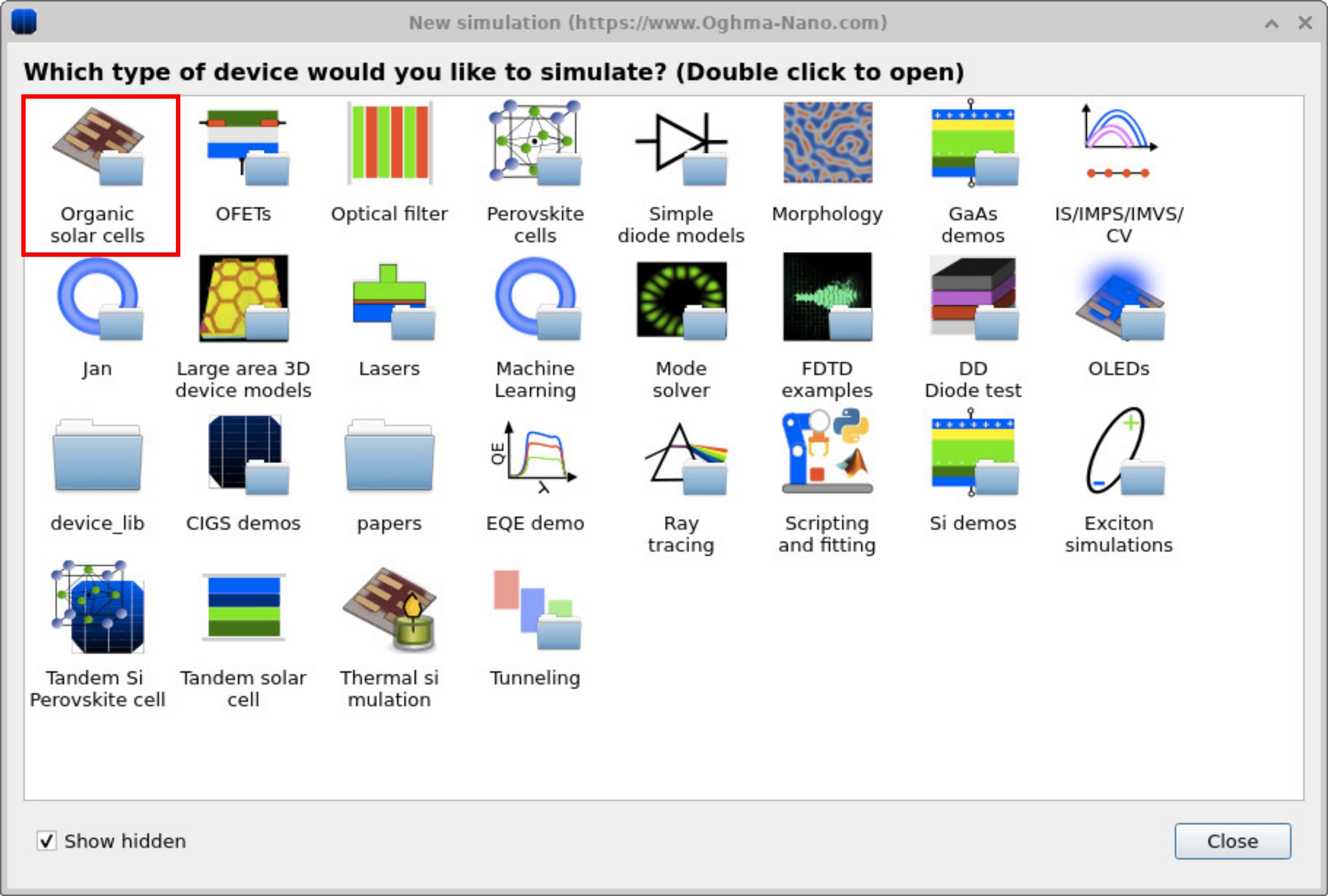
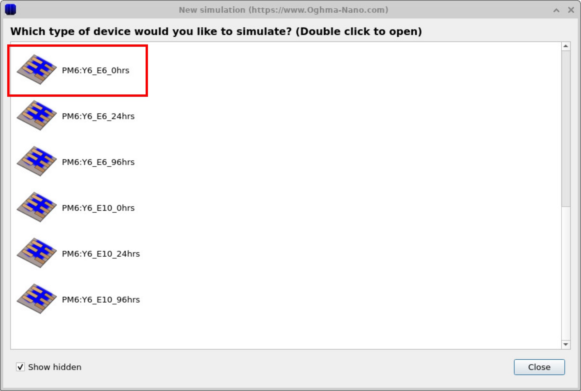
From the New simulation tab in the file ribbon, open the New simulation window (see ??). Choose Organic solar cells, then pick a ready-made PM6:Y6_E6_0hrs demo device to start (see ??). There is nothing special about this device, apart from it has preconfigured Impedance Spectroscopy simulation modes. We will use the FX domain tools to run IS around a nominal operating point.
3. Examine the IS simulation
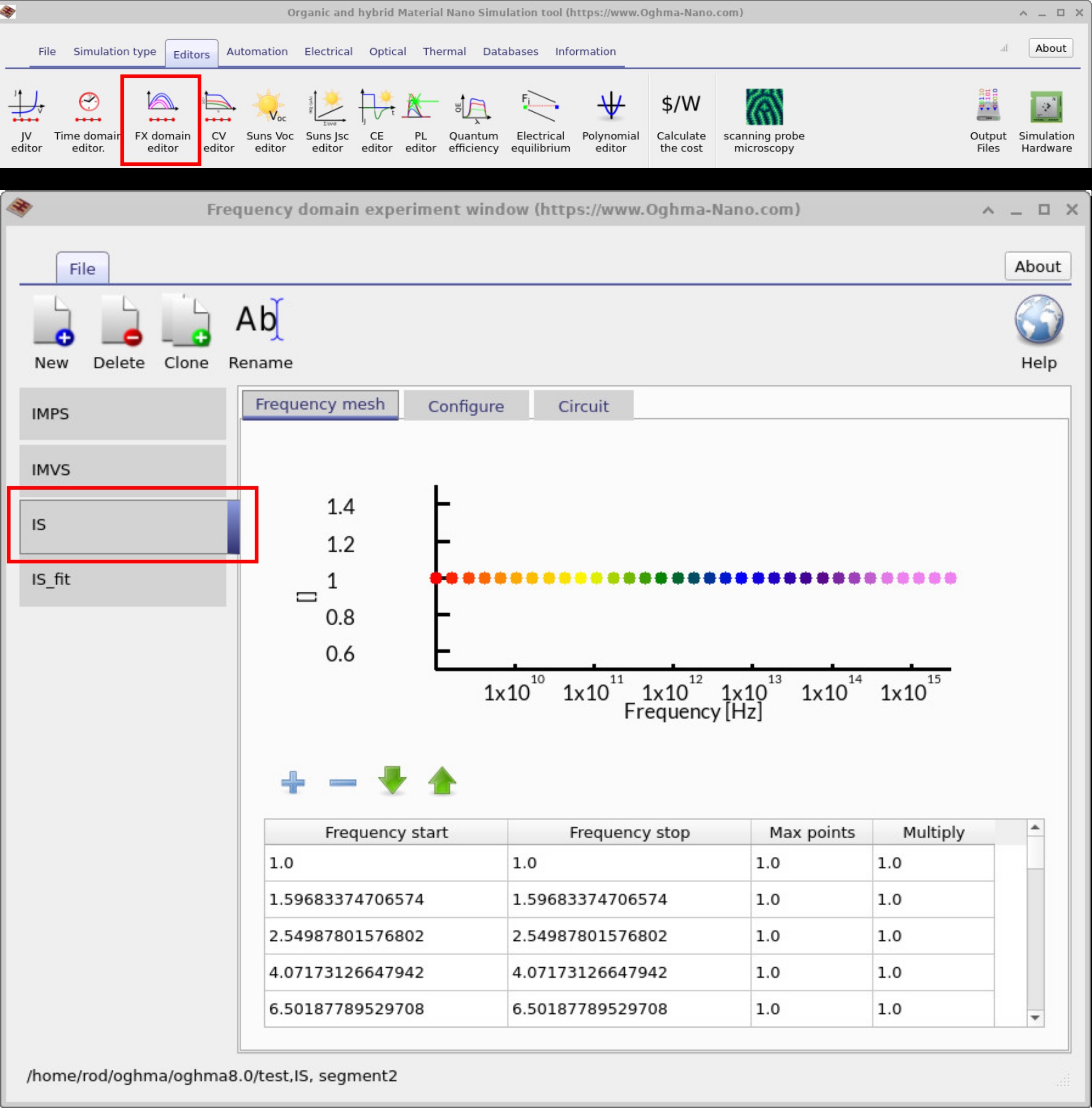
By going to the Editors ribbon in the main window and clicking FX Domain Editor, you will see the frequency domain editor pop up. Click on the IS tab (Impedance Spectroscopy).
If you then look at the Frequency mesh, you can see what frequency points are going to be simulated
(??).
In this example, individual frequency points are listed because the simulation was initially designed to match
an experimental dataset. However, there’s no reason why you can’t define a continuous range with a
start frequency, a stop frequency, and a maximum number of points. If you want the spacing between points to increase, you can adjust the Multiply value from
1.0 to, say, 1.05 or 0.01.
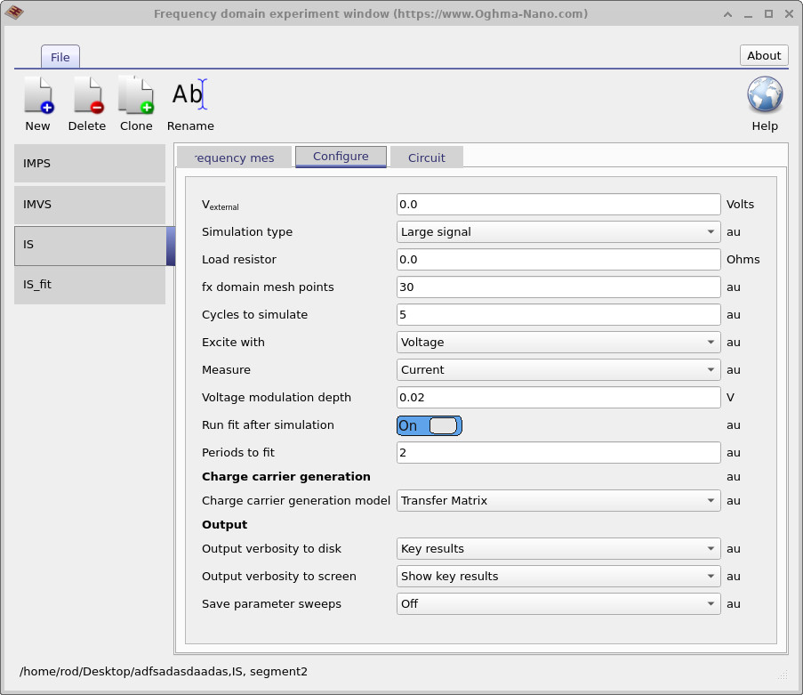
The next figure (??) shows the
Configure tab, which controls how the simulation runs.
Here, an impedance spectroscopy simulation is defined.
The external bias (Vexternal) is set to 0 V, so the device is simulated at short circuit.
The excitation is applied as a voltage, while the measured response is the current.
This setup represents a typical impedance spectroscopy simulation, with a voltage modulation depth of 0.02 V.
These are the key parameters that govern the IS experiment.
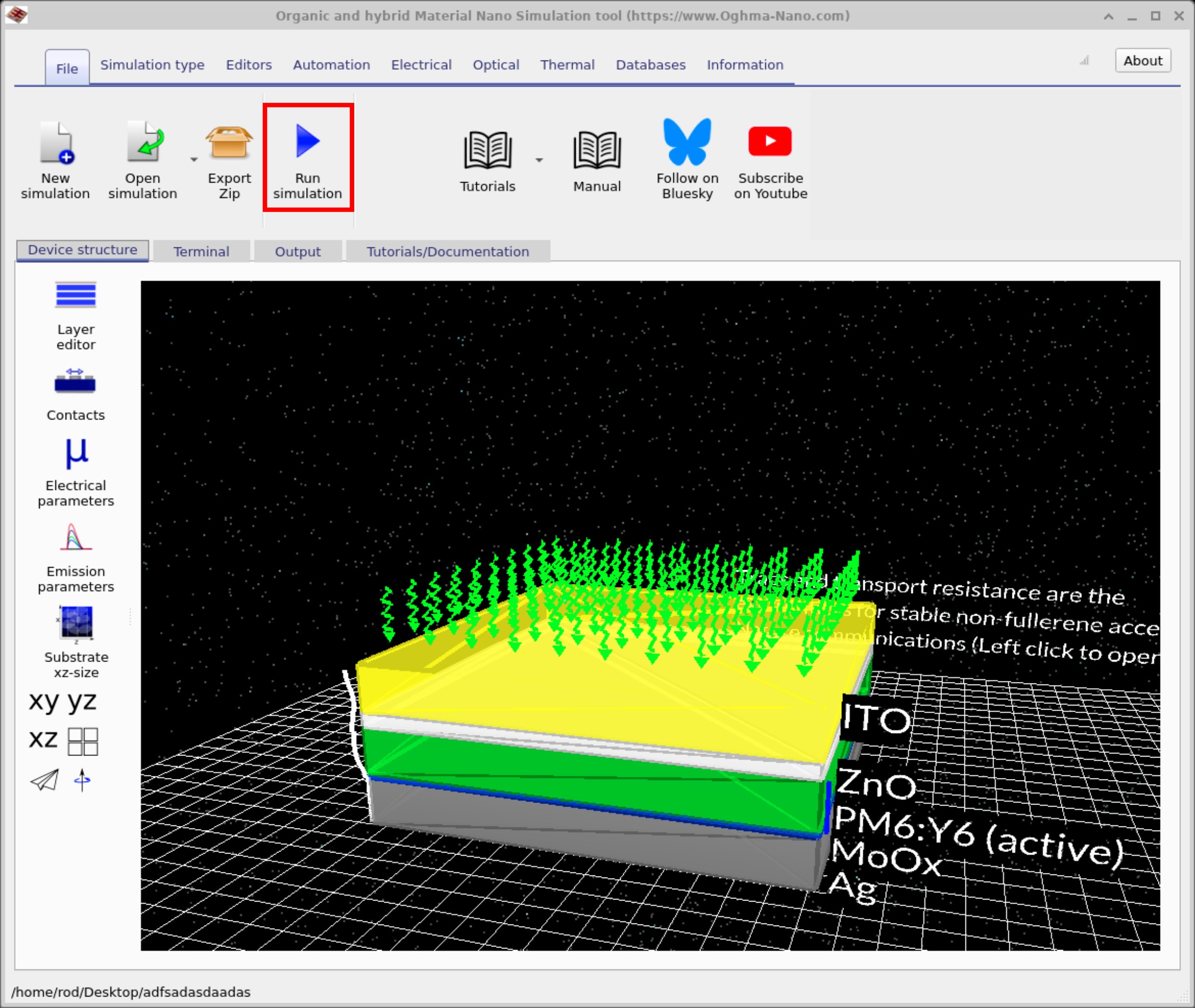
4. Running the simulation and output
As usual, start by returning to the main simulation window and clicking on the File ribbon. Then click Run Simulation (??). Alternatively, you can simply press F9 whilst in the main window.
After the simulation has finished — which may take some time, since it must compute responses across all wavelengths — navigate to the Output tab. Here you will find the various output files generated by the simulation (??).
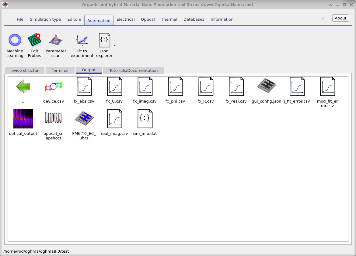
fx_abs.csv, fx_C.csv,
fx_imag.csv, fx_phi.csv, fx_R.csv), along with configuration and fit-error data for further analysis.
5. Reading Bode & Nyquist plots
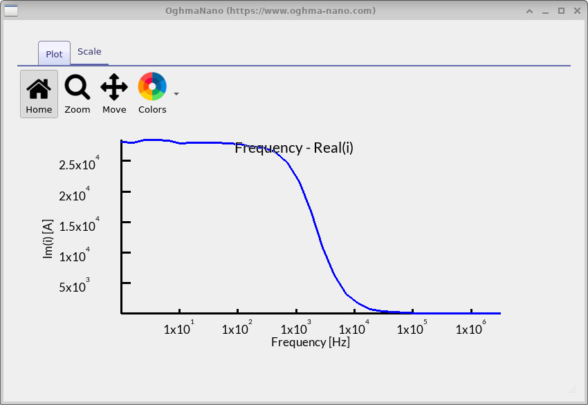
fx_real.csv).
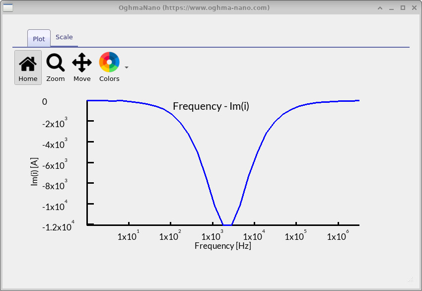
fx_imag.csv).
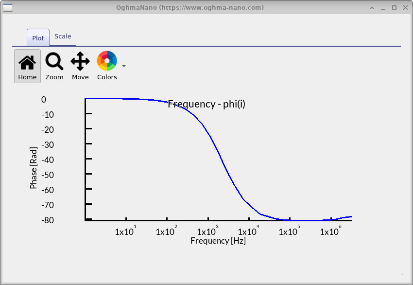
fx_phi.csv).
Once the simulation has finished, you can explore the results by double-clicking the IS output files in the Output tab. Before you begin, note that you can press L while viewing a plot to toggle a logarithmic y-axis, and Shift+L to toggle a logarithmic x-axis. These tools are useful to highlight features more clearly, so try applying them as soon as you open each plot. Each output file corresponds to a different part of the impedance spectrum:
-
fx_real.csv– Bode (real) plot (??): shows the real part of the impedance. At low frequencies this corresponds to the DC resistance of the device, while at high frequencies it flattens to the series/contact resistance. In your results, you can see a drop between \(10^3\)–\(10^4\) Hz where the device stops following the AC changes. -
fx_imag.csv– Bode (imag) plot (??): shows the imaginary part of the impedance. A dip (negative peak) appears around \(10^3\)–\(10^4\) Hz, marking a relaxation process in the device — in other words, the frequency where stored charge can no longer keep up with the applied signal. -
fx_phi.csv– Bode (phase) plot (??): shows the phase difference between the applied voltage and measured current. At low frequency the phase is near 0° (resistor-like behaviour), then drops toward −80° around the same frequency as the imaginary dip, showing capacitive behaviour, and finally returns toward 0° at high frequency (again resistive). -
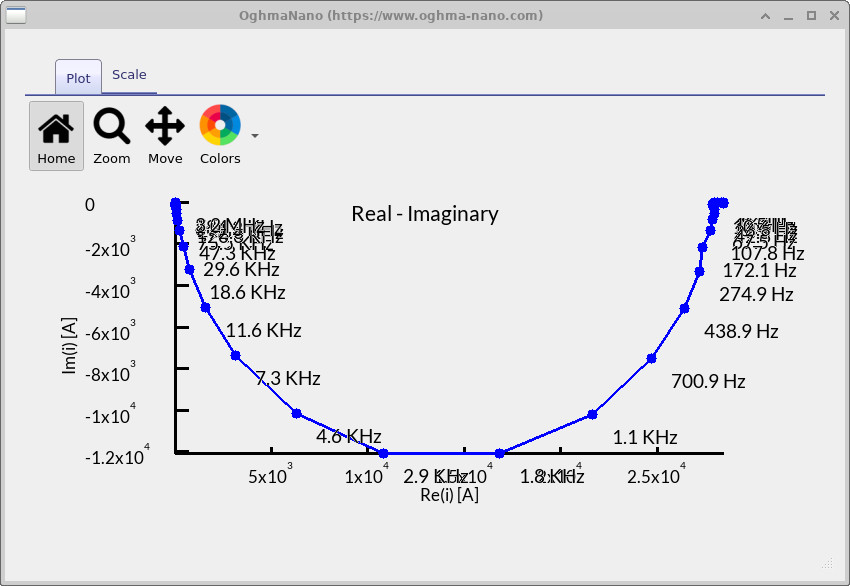
real_imag.csv– Nyquist plot (??): combines the real and imaginary parts into one curve. You can see a large semicircle, the hallmark of an RC process. Its diameter gives the resistance, and the point at the top corresponds to the same frequency region highlighted in the Bode plots. This cross-check confirms that the main feature in this device is a single, strong RC element.
Taken together, these plots show that your device is dominated by a single RC process in the \(10^3\)–\(10^4\) Hz range. At very low frequencies, the impedance is set by the full device resistance; at very high frequencies, it is limited by contact/series resistance. The strong semicircle and matching features across the Bode plots suggest that one particular resistive–capacitive pathway (likely linked to charge storage and transport in the active layer or interfaces) governs the frequency response. In practice, this means the device behaves like a fairly simple RC circuit: resistive at the extremes, with a clear capacitive relaxation process in between. Understanding where that process sits in frequency helps you connect it to the underlying physics — for example, whether the bottleneck is charge transport, interfacial capacitance, or contact resistance.
A summary of all files is given below.
| File name | Description |
|---|---|
fx_abs.csv |
Plot of frequency against the absolute value of current. |
fx_C.csv |
Plot of frequency against capacitance. |
fx_imag.csv |
Plot of frequency against the imaginary component of the current. |
fx_phi.csv |
Plot of frequency against the phase angle. |
fx_R.csv |
Plot of frequency against resistance. |
fx_real.csv |
Plot of frequency against the real component of the current. |
real_imag.csv |
Nyquist plot of the real versus imaginary parts of the current as a function of frequency. |
6. Summary & next steps
In this tutorial you learned how to configure and run impedance spectroscopy (IS) in OghmaNano, inspect Bode and Nyquist plots, and relate their features to device physics. The same methods can be applied to perovskite devices, OFETs, LEDs, and sensors. For deeper analysis, try exporting CSV outputs to fit equivalent circuits or compare with experimental data.
📝 Check your understanding (Impedance Spectroscopy)
- In a Nyquist plot, what does the size and position of a semicircle tell you about resistance and capacitance in the device?
- How can you link the peak in the Bode (imaginary) plot to the top of a Nyquist semicircle?
- What does the Bode (phase) plot reveal about whether the device is behaving more resistively or capacitively?
- What happens to the IS response if you increase or decrease the shunt resistance in the electrical ribbon?
- How do changes in illumination (dark → 1 sun) alter the impedance spectra, and what physical processes do these changes indicate?
💡 Tasks: Explore how IMPS responds to different physical and parasitic changes:
- Series and shunt resistances: In the Electrical ribbon of the main window, open the Parasitic components editor. Increase the shunt resistance up to \(10^{16}\ \Omega\), then reduce it to values such as 100 Ω or 10 Ω, and rerun the IMPS simulation.
- Carrier mobilities: In the Electrical parameters editor of the device structure, adjust the electron and hole mobilities. Try raising them by two orders of magnitude and observe how the IMPS Bode and Nyquist plots shift.
- Illumination level: In the Optical tab of the main window, change the light intensity from 1 sun to dark. Compare the IMPS spectra under illumination versus dark conditions.
✅ Expected results
- Series/shunt resistance: Increasing shunt resistance reduces leakage currents, giving cleaner arcs in the IMPS Nyquist plot. Reducing shunt resistance to ~100 Ω or below increases leakage, flattening the response and lowering the real photocurrent signal across all frequencies.
- Carrier mobilities: Higher mobilities improve charge transport and extraction, shifting the IMPS characteristic frequency (dip in the imaginary part / Nyquist arc peak) to higher values. Lower mobilities broaden and enlarge the arc, moving features to lower frequencies and highlighting transport limitations.
- Illumination: In the dark, IMPS signals are very weak, dominated by background leakage and noise. Under 1 sun, photogeneration boosts the photocurrent response, and recombination introduces distinct features, often sharpening the main arc and shifting phase transitions.
👉 Next steps:
- Continue to Part C: Intensity Modulated Photovoltage Spectroscopy (IMVS) to explore how devices store and release charge, and how recombination dynamics can be extracted from voltage responses under modulated light.
- 📘 Return to the introduction to organic electronics for a broader overview of the topic.