Large-Area Perovskite Module Tutorial Part A: Quick start – open the example and build the circuit mesh
Most device-level simulations in OghmaNano are drift-diffusion simulations, where the solver resolves coupled carrier transport and electrostatics in detail. That physics-first approach is excellent for understanding how a device works, but it becomes computationally too expensive as soon as you move beyond a single cell into large-area devices and modules made from many connected sub-cells.
This tutorial introduces a complementary approach: representing the large-area device as a 3D electrical circuit and solving it using Kirchhoff’s current law and Kirchhoff’s voltage law. Instead of tracking electron and hole currents and the electrostatic potential everywhere, the circuit model tracks the quantities a module engineer usually cares about: current and voltage. This simplification is (i) far more numerically stable at scale, and (ii) fast enough to let you explore realistic module geometries.
Conceptually, the 3D structure is discretised into a set of nodes (points in the device) connected by links that represent circuit elements such as resistors and diodes. Optical generation is included using a quasi-3D transfer-matrix approach: a 1D transfer-matrix calculation is performed through the stack, evaluated across the device area, and the resulting generation profile is coupled into the circuit network. The end result is a practical model for asking upscaling questions like: "My lab-scale device is 20% at 1 mm × 1 mm - what happens when I scale it up into a module, and what becomes the limiting factor?" This is a process we call virtual upscaling.
The experimental inspiration: carbon perovskite "fingers" made into modules
The example module in this tutorial is inspired by experimental work from the Swansea group: Energies 2021, 14, 386, "Triple-Mesoscopic Carbon Perovskite Solar Cells: Materials, Processing and Applications" (Simone M. P. Meroni, Carys Worsley, Dimitrios Raptis, and Trystan M. Watson). You can open the paper via the DOI link here: https://doi.org/10.3390/en14020386.
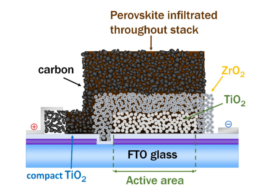
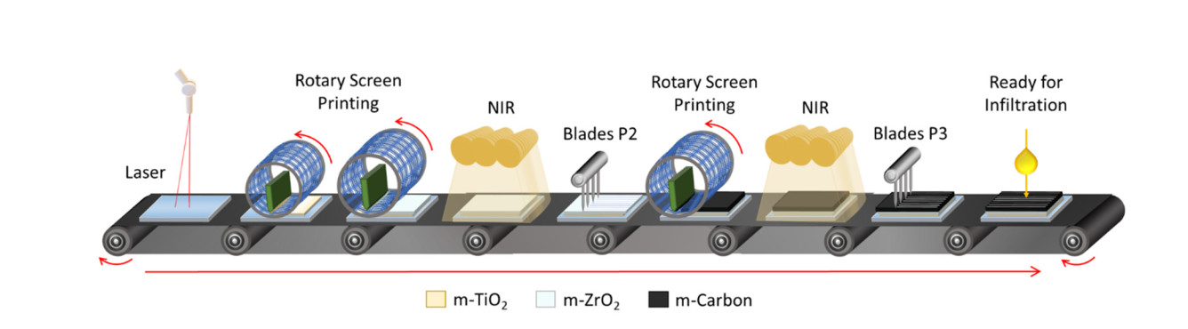
🔗 Paper and licence: The figures above are taken from https://doi.org/10.3390/en14020386. The article is open access and distributed under the Creative Commons Attribution (CC BY) licence: https://creativecommons.org/licenses/by/4.0/ (Copyright: © 2021 by the authors; licensee MDPI, Basel, Switzerland).
Step 1: Create a new perovskite module simulation
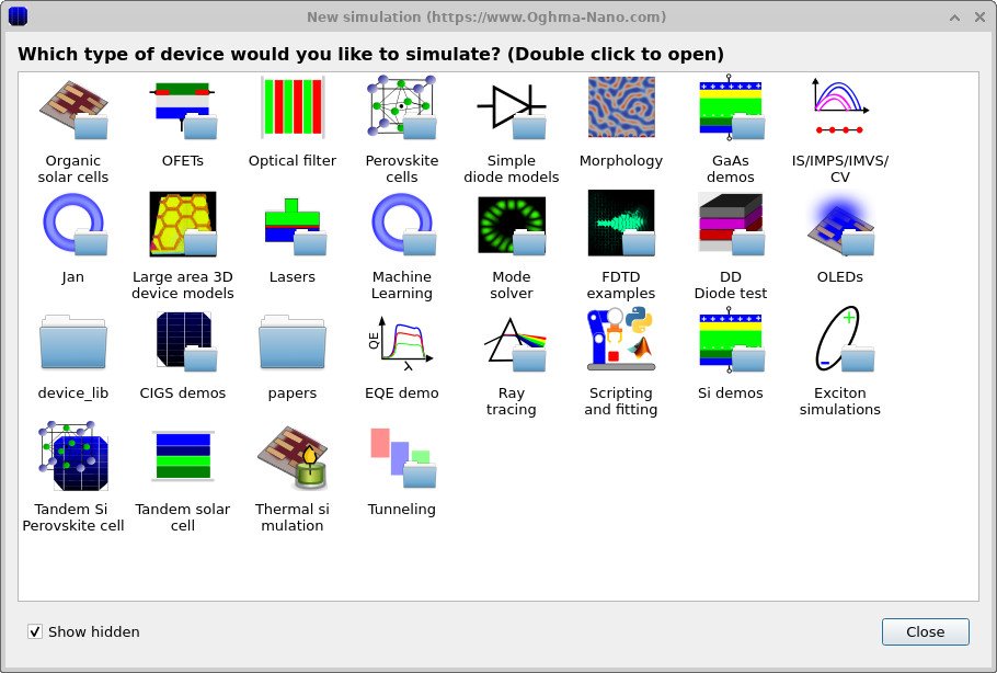
Start from the main OghmaNano window and click New simulation. This opens the device/library chooser shown in
??.
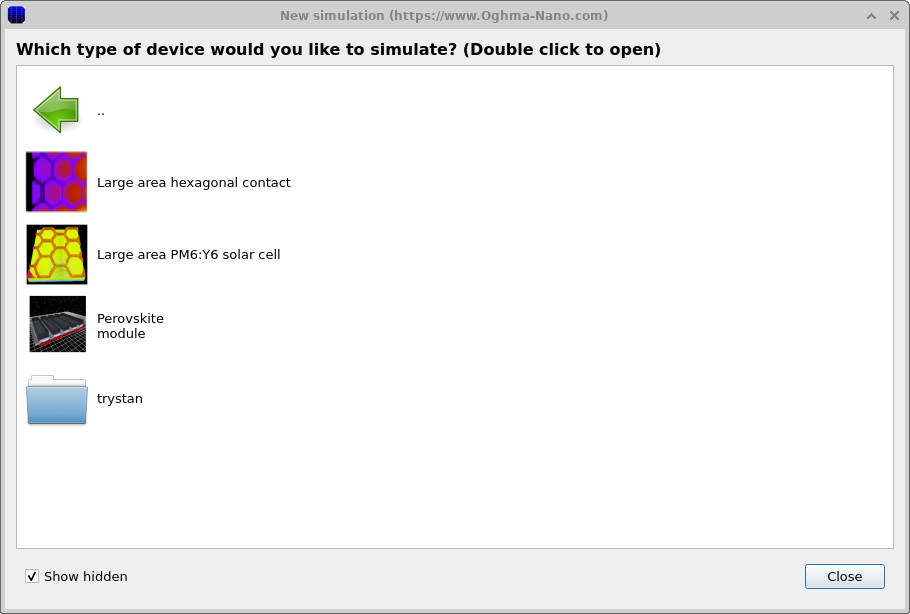
Double-click Large area 3D device modules, then select Perovskite module as shown in
??.
When prompted, save the simulation to a folder you have fast read/write access to (e.g. C:\ on Windows).
💡 Tip: Avoid saving simulations to network drives, USB sticks, or cloud-synchronised folders (e.g. OneDrive). Large-area simulations tend to generate many intermediate files; background sync and network latency can make runs feel unnecessarily slow.
Step 2: Inspect the 3D structure and understand current flow
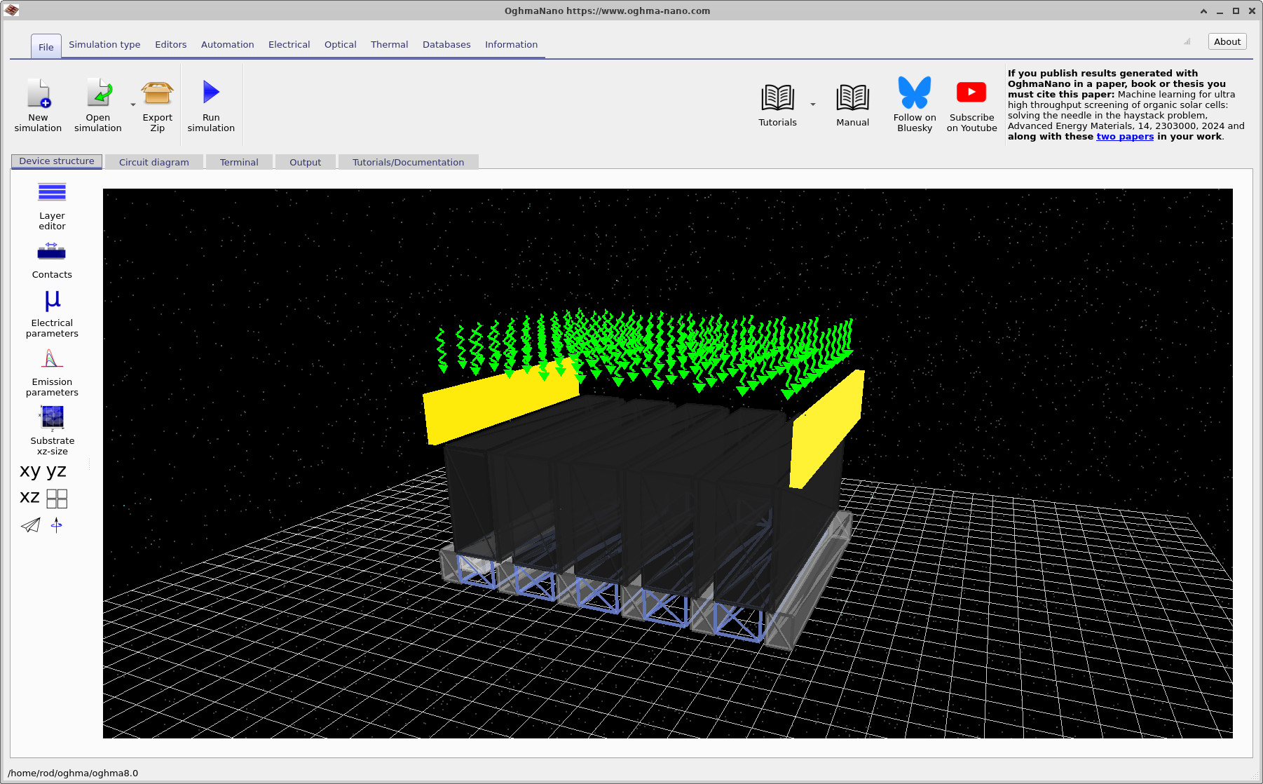
After selecting the template, the main simulation window opens and you will see the 3D device structure (??). This example consists of five fingers - each dark "bar" is an individual solar-cell finger within the larger module geometry.
In this device the dark top region is a carbon contact infiltrated with perovskite (a characteristic feature of this triple-mesoscopic architecture). The module connects the fingers so that the current follows a zig-zag path through the structure. In practical terms, current enters at one side, travels through a contacted region, then is forced to "step" between fingers - up/down and across - until it reaches the terminal on the opposite side.
The contacts can look like they are floating in space (yellow blocks), but they should be interpreted as a contact mask: the region directly underneath is what becomes electrically contacted once the circuit mesh is built. It should be noted that, in this simulation, none of the objects you see are part of the epitaxy. In most devices, the structure is defined in the layer editor, which forms a well-ordered device epitaxy with layers stacked on top of each other, making ordering and positioning the layers much easier. However, in this device, due to its complex nature, all the objects you see on the screen are floating in free space and can be moved with the mouse; collision detection prevents them from being dragged over each other. If objects become stuck, press and hold Shift while dragging to move them freely anywhere. Objects should not overlap, as overlap may lead to numerical problems.
Step 3: Build the circuit mesh from the 3D device
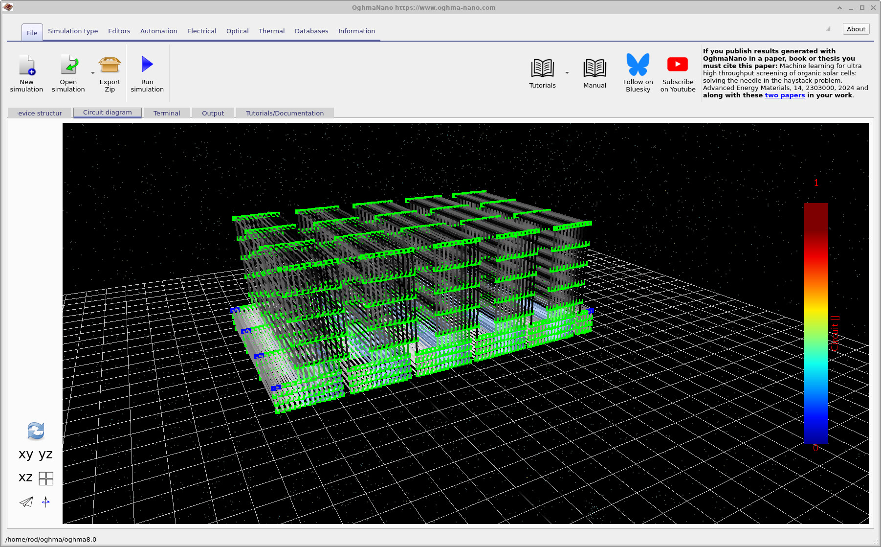
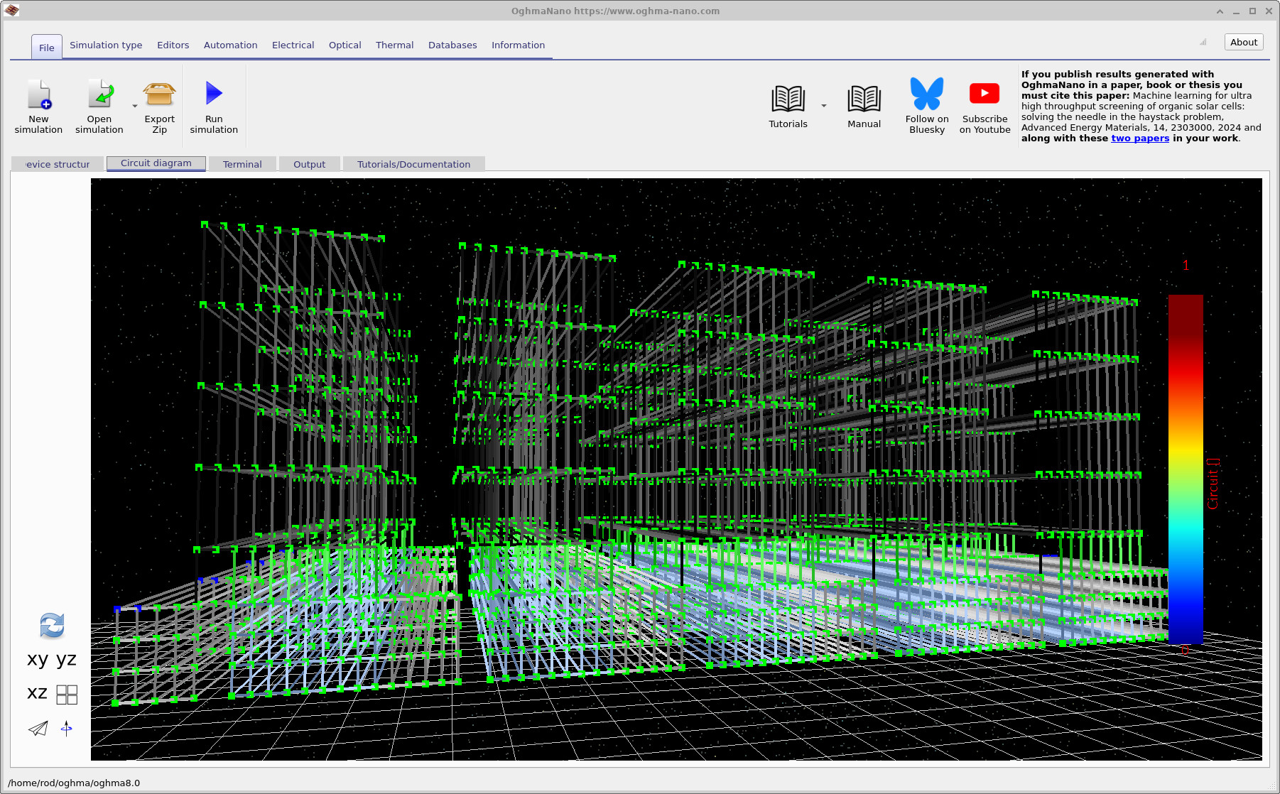
Next, switch to the Circuit diagram tab. In the bottom-left corner you will find a refresh button (it looks like a recycle icon). Click this to build the circuit mesh from the current 3D structure. The initial view is shown in ??.
Rotate the view and zoom in: you will see the mesh links representing the circuit connections across the fingers (?? and ??). If you look closely, you will also notice small blue nodes - these denote contact nodes, and you should see them located directly beneath the yellow contact blocks from the 3D structure view.
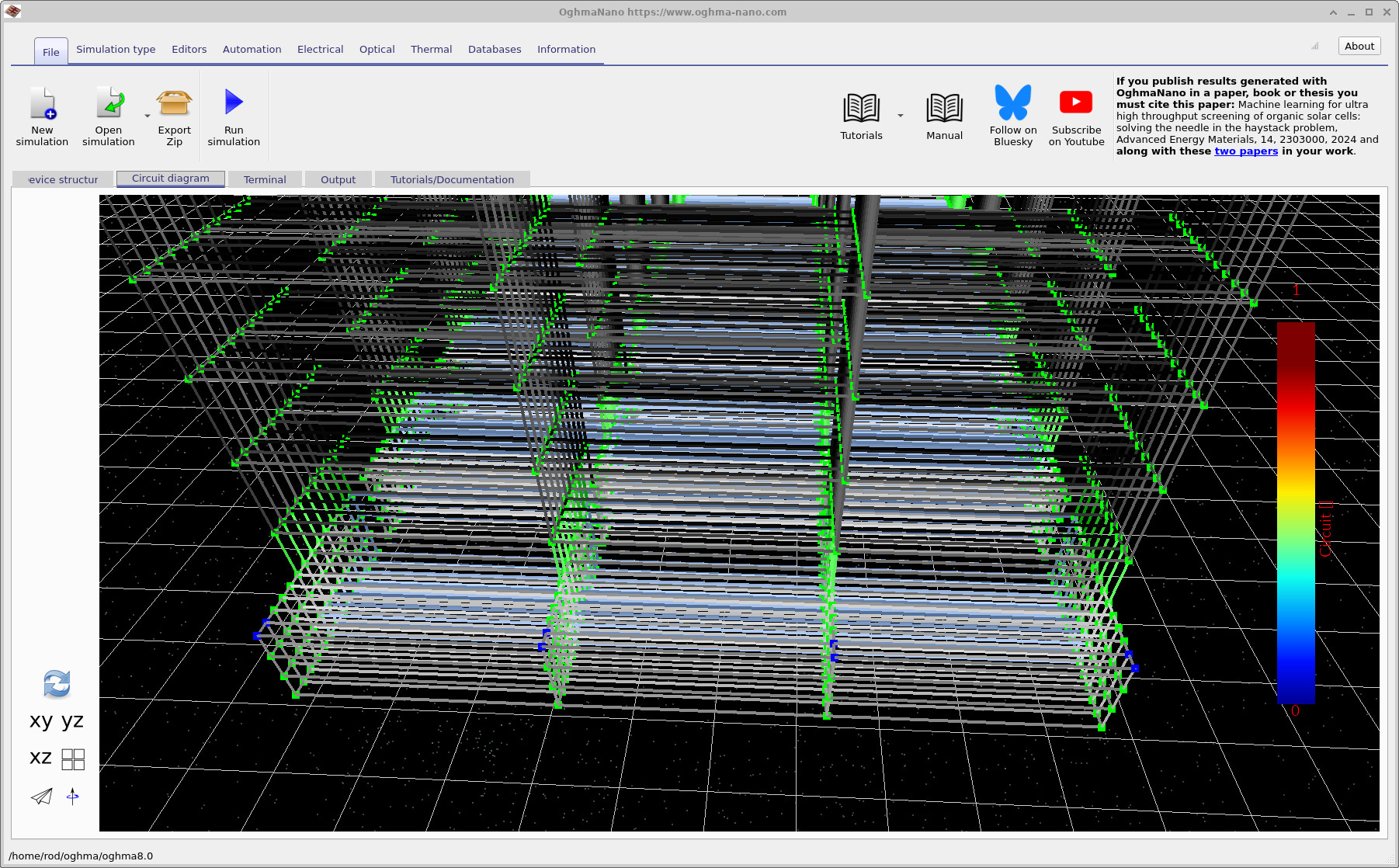
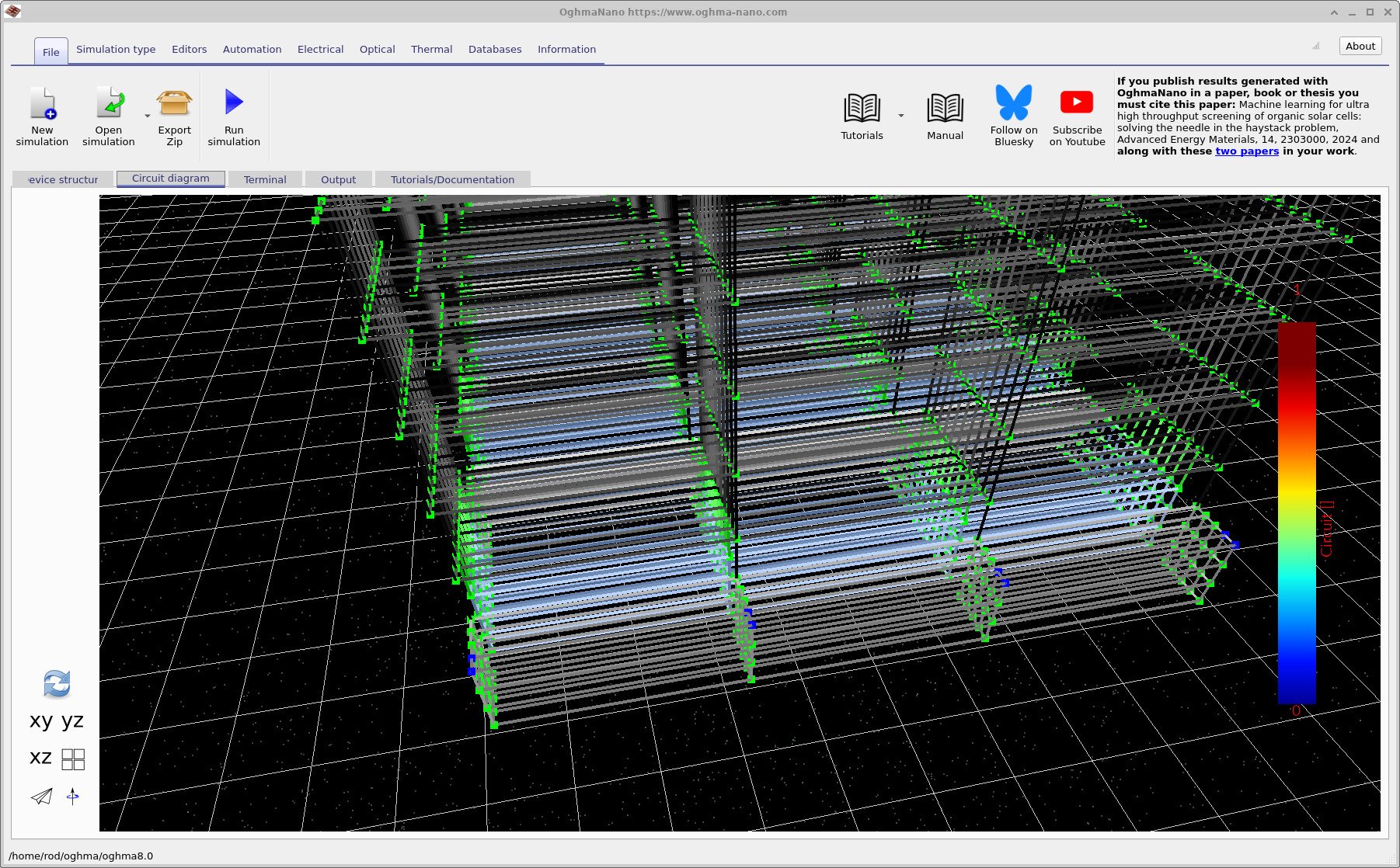
If you spin the device around further you will obtain a view like ??, which makes the multi-finger connectivity and the "zig-zag" collection pathway particularly clear.
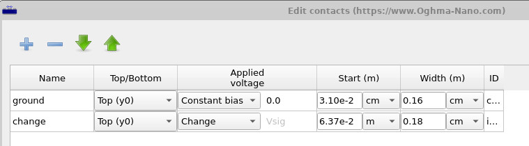
Step 4: Inspect and verify the electrical contacts
To examine contacts directly, open the Contact editor (??). This editor lists the contacts defined for the simulation and shows how they are applied to the device (for example, which side they occupy and what bias is applied). The critical sanity check is simple: the contact definitions here should be consistent with (i) the yellow contact blocks in the 3D view and (ii) the blue contact nodes visible in the circuit mesh.
✅ What to expect
After building the mesh, the Circuit diagram view should show a dense 3D network of links. You should be able to identify blue nodes that represent contacts, and these should sit directly beneath the contact regions defined by the yellow blocks in the 3D structure view. If you do not see contact nodes where you expect them, the most likely causes are: (i) contact regions not overlapping the discretised mesh, or (ii) contacts defined on the wrong side/region in the contact editor.
👉 Next steps:
- Continue to Part B where we explain (in detail) what the circuit model is solving, how optical generation is coupled in, and why this approach is the right tool for module-scale questions.
- Return to the perovskite solar cell simulation guide for the full tutorial overview.