Large-Area Perovskite Module Tutorial Part C: Edit the geometry and upscale your own device
In Part A and Part B you opened the example, built the circuit mesh, ran the simulation, and inspected the outputs. In this final part we will edit the geometry of the device and see how module-level behaviour changes. The key idea is that the module is a 3D circuit model with photogeneration: there is nothing “magical” about it being a perovskite, beyond the optical properties you assign to the active region.
Step 1: Open the Object editor
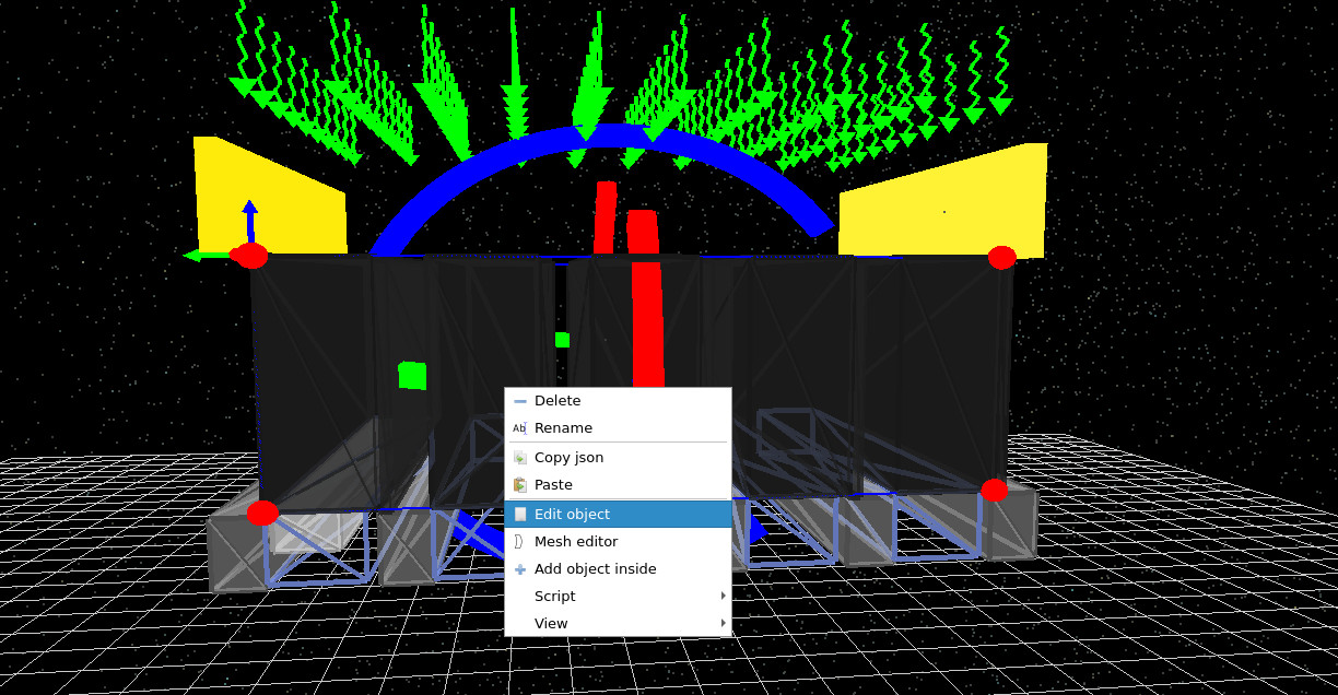
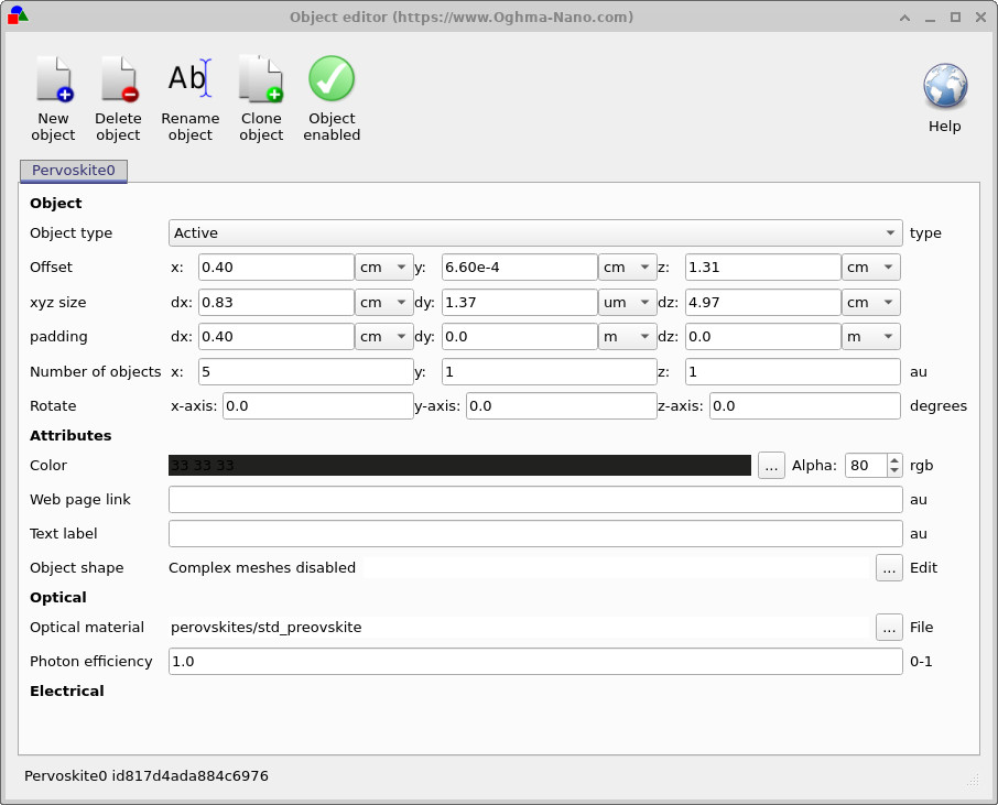
In the 3D view, right-click on the device as shown in ??, then click Edit object. This opens the Object editor shown in ??.
Step 2: Optical material and photon efficiency
In the Optical section of the Object editor
(??),
you will see the current Optical material assignment. In this example it is set to
perovskites/std_perovskite.
This “standard perovskite” material is intended to be representative: in practice, reported optical constants for MAPI/MAPbI3-type materials vary across the literature (different processing, measurement methods, fitting approaches, etc.). Using an averaged/representative absorption spectrum gives a sensible default behaviour without committing to one particular dataset.
You can change the optical material by clicking the ... button next to the optical material field. Note that although this is a “perovskite module” example, the simulation engine here is fundamentally a circuit model + photogeneration. If you change the absorption coefficients, there is nothing stopping you from turning this into a different device class (e.g. an organic absorber) and exploring how it behaves when upscaled.
🧪 Task: Swap the absorber material
- Open the Object editor (??).
- In the Optical material field click ... and select an organic absorber from your materials database.
- Rebuild the circuit mesh (Circuit diagram tab → refresh icon) and rerun the simulation.
- Compare the JV curves to the original perovskite material. What changes most strongly: \(J_\mathrm{SC}\), \(V_\mathrm{OC}\), or the curve shape?
Step 3: What the key geometry fields mean
The Object editor provides a compact set of parameters that define both geometry and how it participates in the electrical mesh:
- Object type = Active: this means the object is electrically active and will take part in the circuit mesh. For the absorber region you want it set to Active, otherwise it will not contribute to the electrical model.
- Offset (x, y, z): the position of the object in space. This is where the object “starts” in the global coordinate system.
- xyz size (dx, dy, dz): the physical dimensions of the object. Notice that the y-size is typically much smaller than x and z because this is a thin-film structure.
- Number of objects: this is the replication feature. You define one object (one set of parameters/materials), and OghmaNano creates carbon-copies of it offset in space. This is exactly what we want for a multi-finger module: all fingers share identical parameters, but are repeated across the device. The important implication is that if you edit the base object, you edit all replicated fingers.
In this example, the absorber region is replicated so that the module has five fingers. If you change the number of objects from 5 → 4, the 3D view should update to show one fewer repeated region (after rebuilding the mesh / refreshing the view as needed).
Step 4: Reduce the module from five fingers to three
Now we will make a controlled geometry change: reduce the number of fingers from five to three. This is a good “stress test” because it forces you to edit both the geometry and the contacts, then validate that the circuit mesh is still connected.
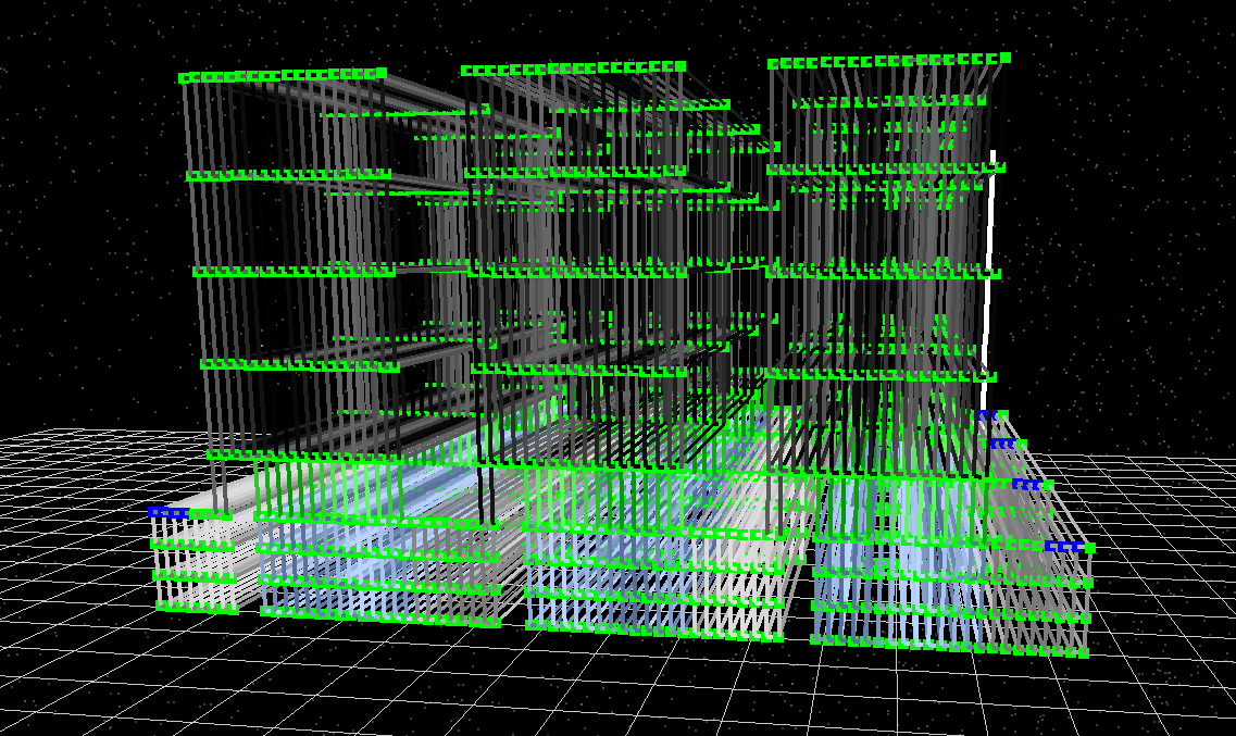
The target outcome is a mesh that looks like ??.
Step 5: Debugging mesh connectivity (what can go wrong)
Once you start editing geometry, it is very easy to create a subtle connectivity problem: a gap, a missing overlap, or a region that is not actually linked into the circuit. An example of this kind of problem is shown in ??, where there is a visible gap and therefore no link path from one region of the device to another.
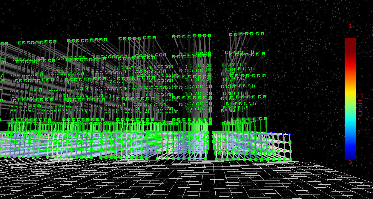
The important point is that if you have created a disconnected circuit, the solver may still try to iterate and you may see odd convergence behaviour, but the results will not be physically meaningful. The fastest way to debug this is simply: rebuild the mesh and inspect it visually. If the mesh is connected and the contacts are where you think they are, the simulation is usually fine.
💡 Debug rule: if the circuit mesh is correct, the solve is usually fine. If the circuit mesh is wrong, the solve is not worth interpreting. Always inspect the mesh carefully after geometry edits.
What to do next
You now have the core workflow: start from a small-device parameter set (materials + resistances), build a module geometry, generate the circuit mesh, run, and inspect JV/contact currents and mesh connectivity.
👉 Next step: Try upscaling your own device
Find parameters from one of your own small-area devices (e.g. sheet resistances of electrodes/contacts, diode parameters, and absorber optical constants), put them into the model, and run the same module geometry. Then ask: what becomes the limiting factor when you scale up? In many cases it is not the intrinsic “cell efficiency”, but module-scale effects such as lateral conductivity of electrodes, contact resistances, or geometry-dependent current crowding.
Well done! You’ve completed the perovskite module tutorial - including editing geometry, rebuilding the circuit mesh, and validating connectivity 🎉
👉 Next steps:
- Return to the perovskite solar cell simulation guide for the full tutorial overview.