Large-Area Perovskite Module Tutorial Part B: Run the simulation and inspect the outputs
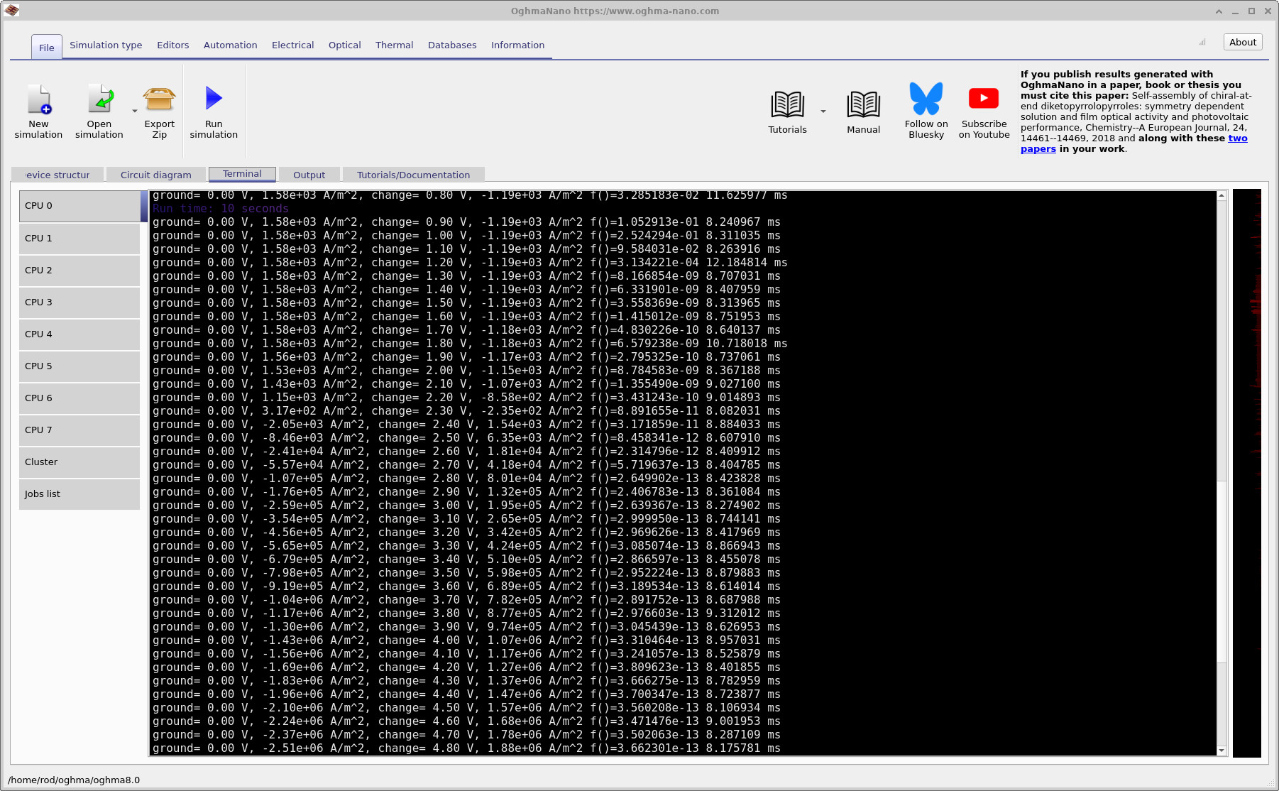
Large-area module simulations are more complicated than a single-device drift–diffusion run, so it is worth watching what the solver is doing. In this example, OghmaNano runs the simulation in two main stages: (i) the optical solver (3D optical calculation), then (ii) the electrical circuit solver (Kirchhoff current/voltage equations on the circuit mesh). The terminal output is your quickest way of spotting problems early (for example, a disconnected circuit or missing contacts).
Step 1: Run the simulation
Click the Run simulation button (blue triangle) shown in ??. This simulation will take a while to run (it is doing a 3D optical stage followed by a large circuit solve). While it runs, keep an eye on the Terminal tab, because it provides real-time information about convergence and currents.

Step 2: Understand what the terminal output is telling you
For these complicated simulations, the terminal output is not “noise” - it is a diagnostic. In ?? you can see that the solver initially runs the optical stage. This can take a while because it is solving in 3D. Once optical generation is prepared, the solver starts the electrical stage and prints lines for each bias point.
A key line looks like this (format will vary slightly depending on settings):
- Contact voltages: e.g.
ground = 0.00 Vmeans the ground contact is held at 0 V;change = 0.10 Vmeans the other contact is at 0.10 V. - Contact currents: e.g.
1.58e+03 A/m^2on one contact and-1.19e+03 A/m^2on the other means current flows into one contact and out of the other. At 0 V, that is essentially the module’s short-circuit current density (JSC), because the device is illuminated and delivering current at zero applied voltage. - Convergence metric: the printed
f()value is the solver’s error/residual for the electrical solve (the Kirchhoff-law equations over the entire circuit mesh). You can loosely think of it as “how well the circuit equations are satisfied” across the full network. - Per-step time: the last number on the line (milliseconds) is the time taken to solve that bias point.
You will often see higher error near the start of a sweep (especially near 0 V), and the error may drop as the solver moves away from that point. As a rule of thumb, I trust results far more when the solver is reaching errors like 10-4 or smaller, and ideally down to 10-9 for “clean” convergence. (In the example logs shown here you can see the error trending downward as the sweep progresses.)
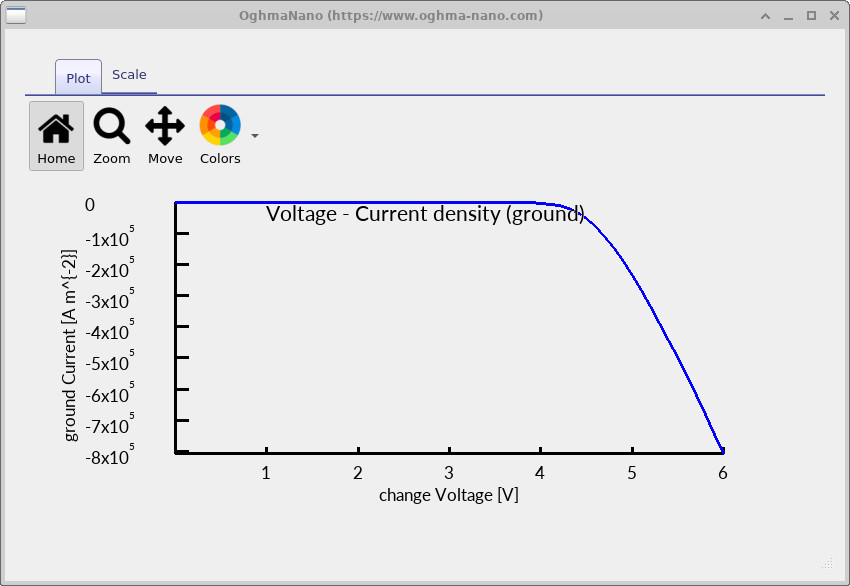
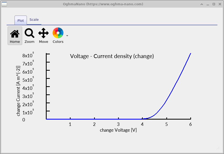
In ?? you can see something very useful:
about midway through the sweep the current on the ground contact changes sign, and the current on the change contact changes sign in the opposite direction.
That sign flip is exactly what you expect as the sweep passes VOC: below VOC the illuminated device sources power;
above VOC it is forward-biased and consumes power like a diode.
In other words, you can often “see” the JV curve forming directly in the contact-current column.
💡 Why watch the terminal? If something is wrong (e.g. the circuit is not connected, a contact mask missed the mesh, or a region is floating),
you will usually see it immediately: currents collapse toward zero, currents become nonsensical, or the solver fails to reduce f().
Catching that early can save you a long wait.
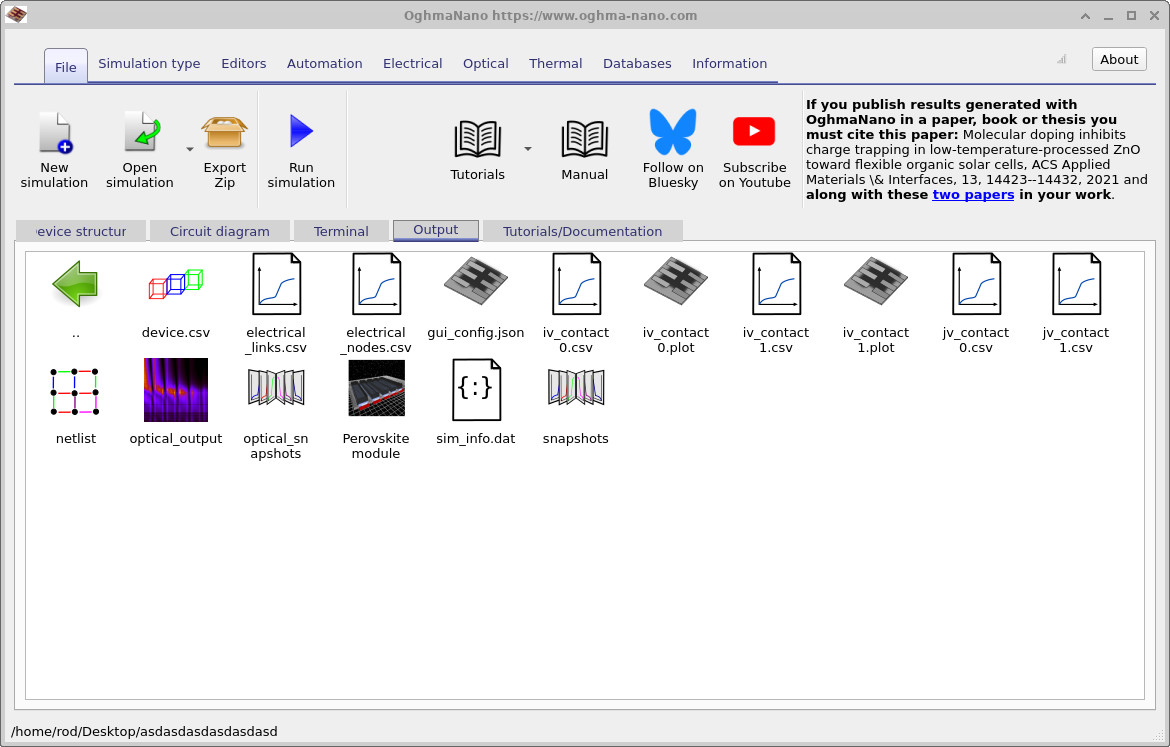
Step 3: Inspect the output files
When the simulation finishes, the Output tab will contain a set of files like those shown in
??.
The key results for this part of the tutorial are the contact JV curves:
jv_contact0.csv and jv_contact1.csv.
These contain the current density at each contact as a function of the applied voltage.
Double-click jv_contact0.csv and jv_contact1.csv to plot them. Example plots are shown in
?? and
??.
A zoomed-in view (useful for reading off VOC and the curvature near the knee) is shown in
??.
jv_contact0.csv).
jv_contact1.csv).
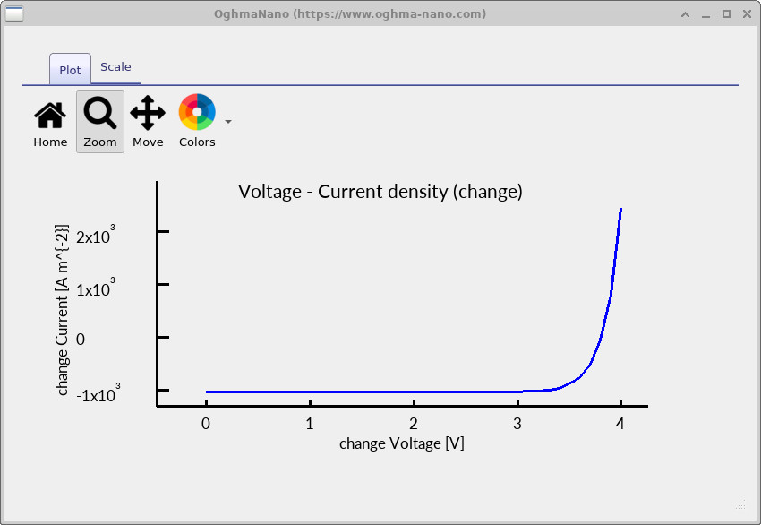
✅ What to expect
Under illumination, at 0 V you should observe a non-zero current magnitude at the contacts (the module’s JSC). As voltage increases, the current approaches zero around VOC, then changes sign in forward bias. If the JV curves look flat (near-zero everywhere), that usually indicates a disconnected circuit, missing contacts, or a geometry/contact-mask mismatch.
Step 4: Inspect the solver mesh and circuit representation
Large-area simulations can fail for geometrical reasons (misplaced contacts, missing regions, unintended gaps), so it is useful to know where to look. In particular:
device.csv- this is a view of the mesh the solver actually sees. The nicely rendered 3D view in the GUI is not what the solver uses internally. The solver operates on a more rudimentary triangular representation, and if something is wrong with the geometry, it will usually be visible here.electrical_links.csv- lists the circuit links (the elements connecting nodes: resistive paths / diode connections etc.).electrical_nodes.csv- lists the Kirchhoff nodes used in the solve (the points where currents sum to zero).
Example views of these files are shown in ??, ??, and ??. Conceptually, this is the same as solving a standard circuit: nodes + links + Kirchhoff’s laws - just at much larger scale.
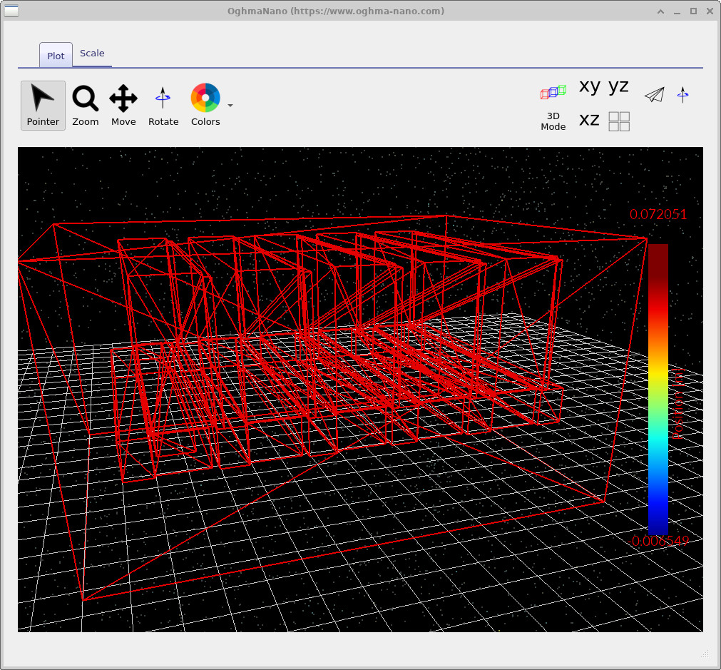
device.csv: the simplified mesh representation used by the solver.
If something is geometrically wrong, it is often obvious here.
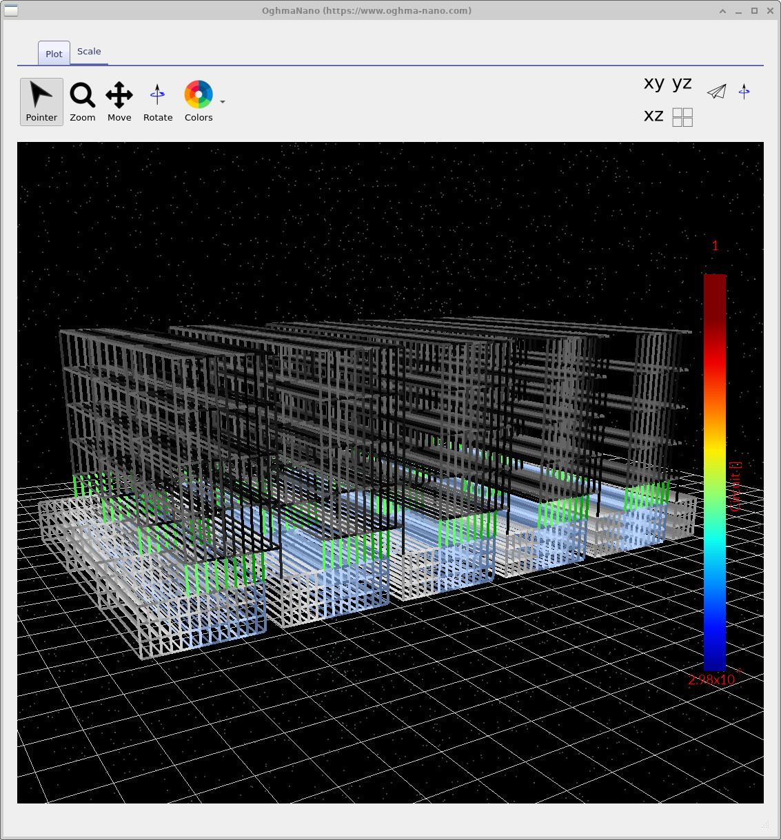
electrical_links.csv: the circuit links used in the Kirchhoff solve.
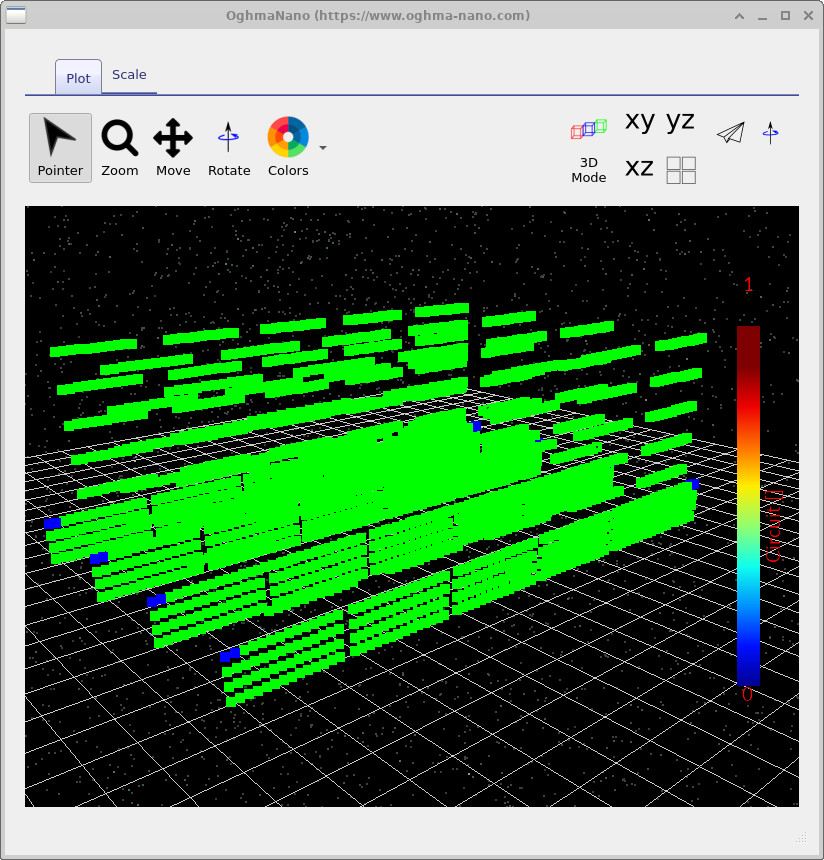
electrical_nodes.csv: the Kirchhoff current nodes used for computation.
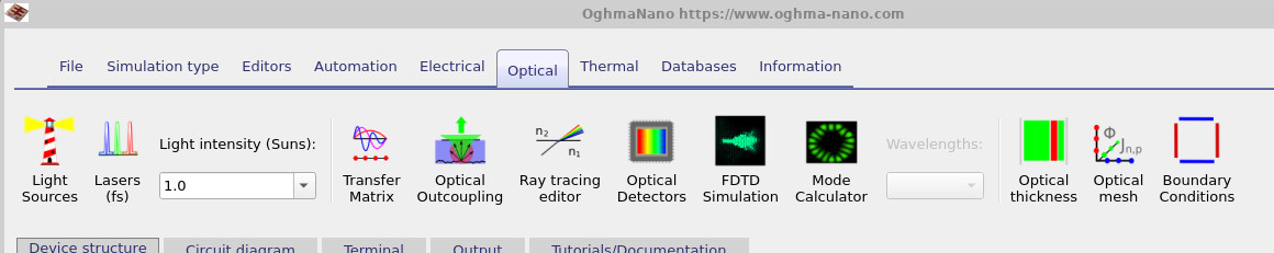
Step 5: Locate the optical settings (Transfer Matrix)
This module simulation includes optical generation, and you can find the optical tools in the Optical ribbon (??). Click Transfer Matrix to open the Transfer Matrix window.
Important: do not run the Transfer Matrix tool from here for this tutorial. The Transfer Matrix window is fundamentally a 1D view through the stack, whereas this simulation is 3D. It is useful for configuration and sanity-checking materials/stack settings, but it is not a substitute for the full 3D optical stage you just ran. For now, open it and click Configure - we will use this entry point in Part C when we start making controlled changes.
Step 5: Locate the optical settings (Transfer Matrix)
This module simulation includes optical generation, and you can find the optical tools in the Optical ribbon (??). Click Transfer Matrix to open the Transfer Matrix window.
Important: do not run the Transfer Matrix tool from here for this tutorial. The Transfer Matrix window is fundamentally a 1D view through the stack, whereas this simulation is 3D. It is useful for configuration and sanity-checking materials/stack settings, but it is not a substitute for the full 3D optical stage you just ran.
Instead, click the Configure (cog) option to open the optical configuration panel shown in ??.
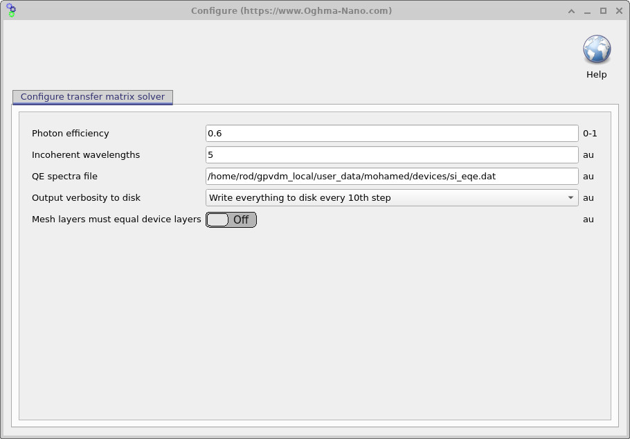
Photon efficiency and the solar-cell diode equation
The photon efficiency (sometimes called an internal quantum efficiency factor in this simplified context) is a scalar multiplier that tells the model what fraction of absorbed photons actually generate extractable charge carriers (electrons and holes). If the photon efficiency is 0, there is no photocurrent. If it is 1, then (in this simplified picture) every absorbed photon contributes to photocurrent. In most real devices, a value around 0.6 is a reasonable order-of-magnitude.
In diode language, you can think of it as scaling the photocurrent term in the illuminated diode equation:
Here, \(J_0\) is the diode saturation current density, \(n\) is the ideality factor, and \(J_{\mathrm{ph}}\) is the photocurrent density predicted from the optical model (i.e. from the absorbed-photon/generation calculation). The parameter \(\eta_{\mathrm{ph}}\) is the photon efficiency from ??, which simply scales the contribution of the photocurrent term. Setting \(\eta_{\mathrm{ph}}=0.6\) means “60% of absorbed photons become extractable carriers” in this effective model.
Practically: if your simulated \(J_\mathrm{SC}\) is badly mismatched to experiment and you are confident the electrical part of the circuit model is sensible, \(\eta_{\mathrm{ph}}\) is one of the quickest knobs you can use to bring the absolute current level into line. It is very unlikely to be above 1; if you find you need \(\eta_{\mathrm{ph}} > 1\), that usually indicates something else is wrong (for example, optical constants / absorption coefficients are not consistent).
🧪 Task: Explore photon efficiency
- Open the Optical ribbon and go to Transfer Matrix → Configure (??).
- Change Photon efficiency from 0.6 to a lower value (e.g. 0.3), rerun the simulation, and observe how the contact JV curves change.
- Try a higher value (e.g. 0.9) and rerun. What happens to \(J_\mathrm{SC}\) and the overall JV curve shape?
- After finishing, set Photon efficiency back to 0.6.
👉 Next steps:
- Continue to Part C where we start altering parameters and interpreting module-scale losses (series resistance, contact limitations, and optical generation effects).
- Return to the perovskite solar cell simulation guide for the full tutorial overview.