

Silicon/SiGe Quantum Well: Six-Band Luttinger–Kohn Hole Tutorial
1. Introduction
Our silicon Δ-valley tutorial examined the electrons in a Si/SiGe quantum well. This tutorial examines the other side of its electronic structure: holes in the valence band. Although the layer stack is similar, the underlying physics is quite different. An electron near an individual silicon conduction valley can be described using an anisotropic effective mass; the top of the valence band contains several nearby, interacting states. A single hole parabola therefore misses important information.
Here we use OghmaNano's six-band Luttinger–Kohn (LK6) model to calculate confined hole subbands in a 10 nm silicon well between two 20 nm SiGe layers. We then follow the calculation beyond the band energies: the example also evaluates acoustic-phonon scattering, hole occupation and the resulting in-plane mobility. You can use the supplied default example without building the structure from scratch.
2. Opening the six-band example
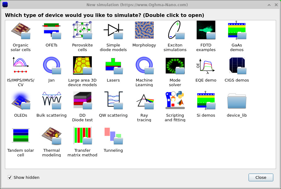
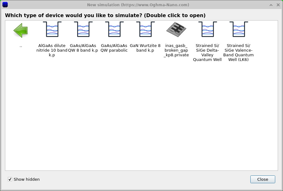
Select File → New simulation. In the example browser, double-click GaAs demos (??). This folder also contains the semiconductor quantum-well templates, including silicon examples. Double-click Strained Si/SiGe Valence-Band Quantum Well (LK6) in the next window (??). Be careful to choose the Valence-Band example: the neighbouring Delta-Valley template calculates silicon conduction electrons instead.
3. Inspecting the Si/SiGe structure and material parameters
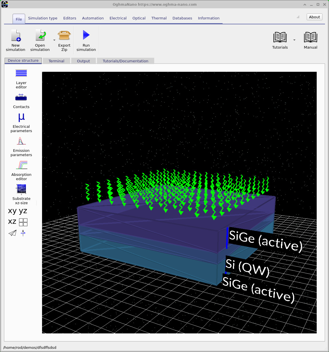
The main window provides a three-dimensional representation of the example (??). The charge carriers are confined through the layers, which we call the z direction, but retain freedom of motion in the x–y plane. Click Layer editor to see the actual thicknesses and the assignment of the central layer as a quantum well.
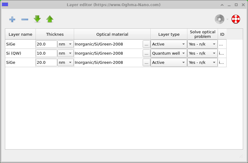
| Layer | Thickness | Role |
|---|---|---|
| SiGe | 20 nm | Surrounding layer |
| Si (QW) | 10 nm | Confined valence states |
| SiGe | 20 nm | Surrounding layer |
The optical-material column shown in ?? is not a substitute for inspecting the electronic material definitions. Band-edge offsets, alloy composition and any strain settings affect the actual confinement potential, so retain the example's supplied configuration for your first run.
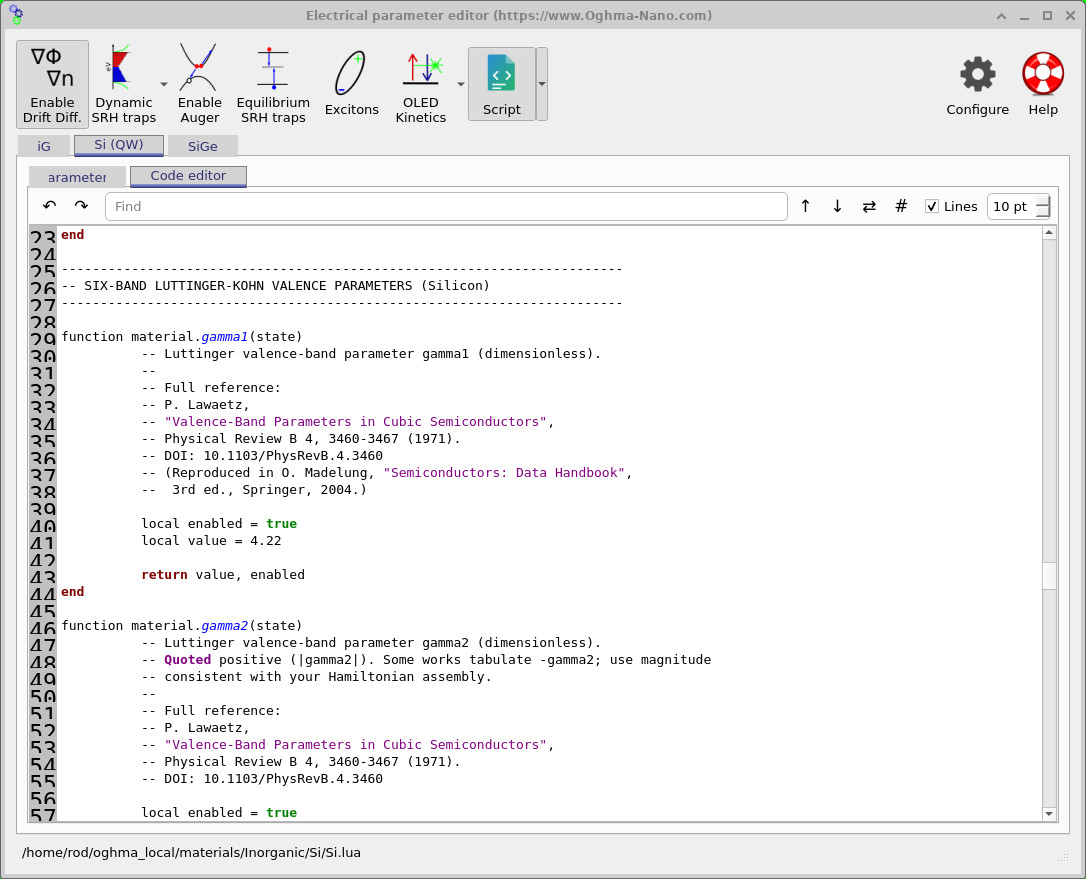
Open Electrical parameters and select Si (QW) (??). The screenshot shows the Luttinger parameter gamma1 and its literature reference. Unlike a one-band electron model, the valence-band calculation uses three Luttinger parameters to describe its coupled heavy-hole, light-hole and split-off branches. It also requires the spin–orbit splitting and, where strain is enabled, suitable deformation-potential parameters.
4. Why does the valence band need six components?
Near the silicon valence-band maximum there are two familiar families of hole states: heavy holes (HH) and light holes (LH). A lower-lying split-off (SO) family arises through spin–orbit interaction. Each family has two spin-related basis states, giving the six components in the LK6 model. These are basis components of a coupled wavefunction, not necessarily six independently moving parabolic bands.
The quantum-well envelope can be represented schematically as a six-component column vector,
\[ \Psi(z)=\begin{pmatrix} F_{\mathrm{HH}+}(z) & F_{\mathrm{LH}+}(z) & F_{\mathrm{SO}+}(z) & F_{\mathrm{HH}-}(z) & F_{\mathrm{LH}-}(z) & F_{\mathrm{SO}-}(z) \end{pmatrix}^{\!T}. \]
Here the labels indicate the principal character of the underlying angular-momentum basis. As in-plane momentum changes, the components generally mix, so an eigenstate initially described as HH-like need not remain purely heavy-hole-like at larger wavevector. The problem solved by the computer is of the form
\[ \left[H_{\mathrm{LK}}(k_x,k_y,-i\partial_z) +H_{\mathrm{BP}}(\varepsilon)+V_v(z)I_6\right]\Psi =E(k_x,k_y)\Psi. \]
The Luttinger–Kohn term describes the kinetic energy and mixing of the valence states; the Bir–Pikus term describes their response to strain; and \(V_v(z)\) represents the valence-band confinement profile. The model retains coupling between the basis components, rather than assigning an independent constant mass to HH, LH and SO. You do not need to assemble this matrix manually for the tutorial; see the LK6 theory page for the detailed Hamiltonian.
For comparison, even a simplified bulk approximation illustrates why the three Luttinger parameters matter: along a cubic principal direction, the heavy- and light-hole curvatures are related to different combinations of the parameters, schematically
\[ \frac{m_0}{m_{\mathrm{HH}}^{*}}\simeq\gamma_1-2\gamma_2, \qquad \frac{m_0}{m_{\mathrm{LH}}^{*}}\simeq\gamma_1+2\gamma_2. \]
These are useful illustrative limiting relations, not an instruction to replace the complete six-band quantum-well calculation by two separate parabolas. In the confined structure, well width, spin–orbit coupling, strain and in-plane momentum determine the actual eigenvalues and their changing state character.
5. Running the calculation
Return to the File ribbon and press Run simulation.
OghmaNano first solves the confined LK6 valence states across a sequence of in-plane wavevectors.
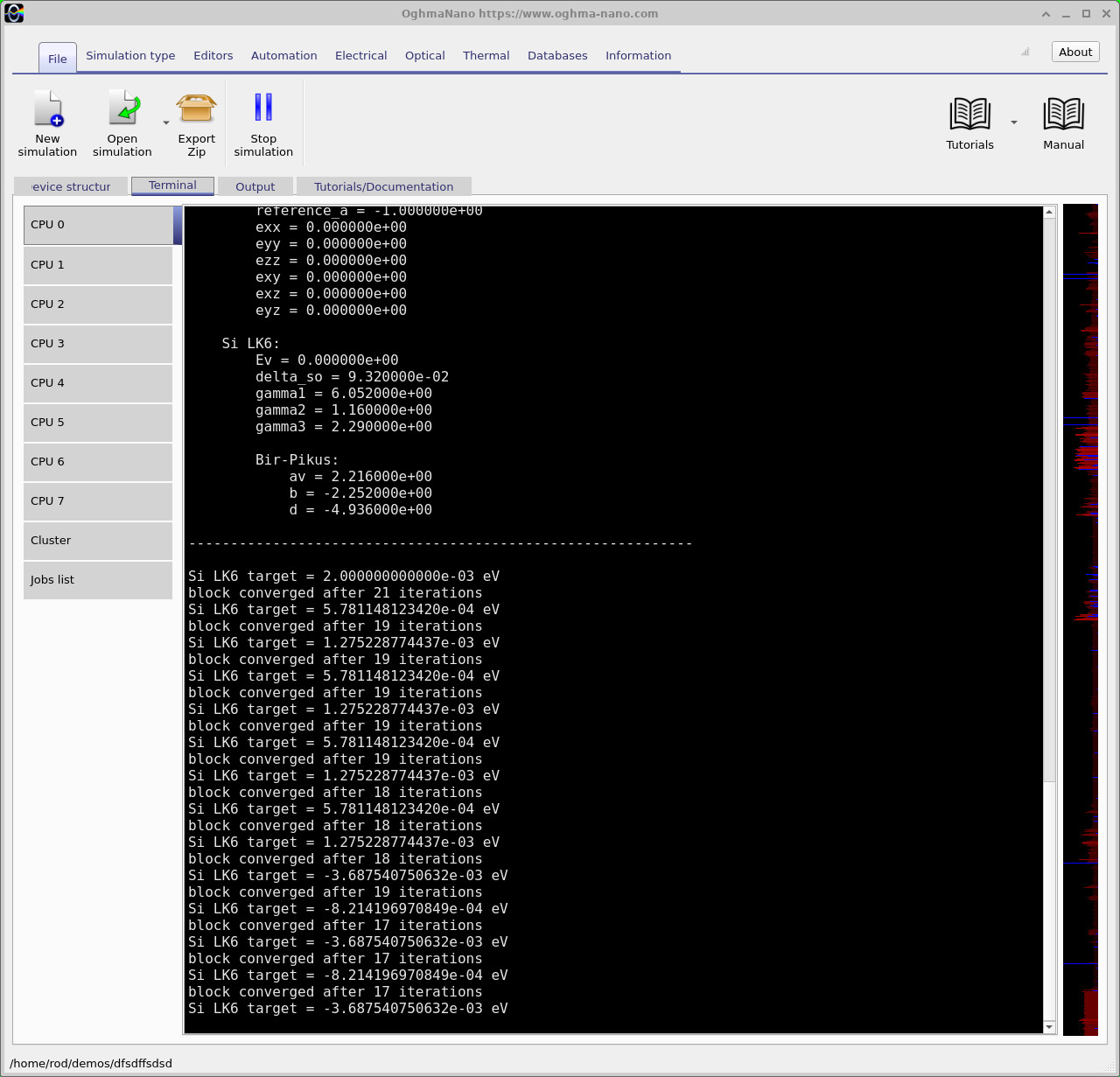
You can follow the calculation in the Terminal tab
(??).
The displayed target energies are internal eigensolver targets; the reported
convergence messages indicate that the requested eigenstates have been found numerically.
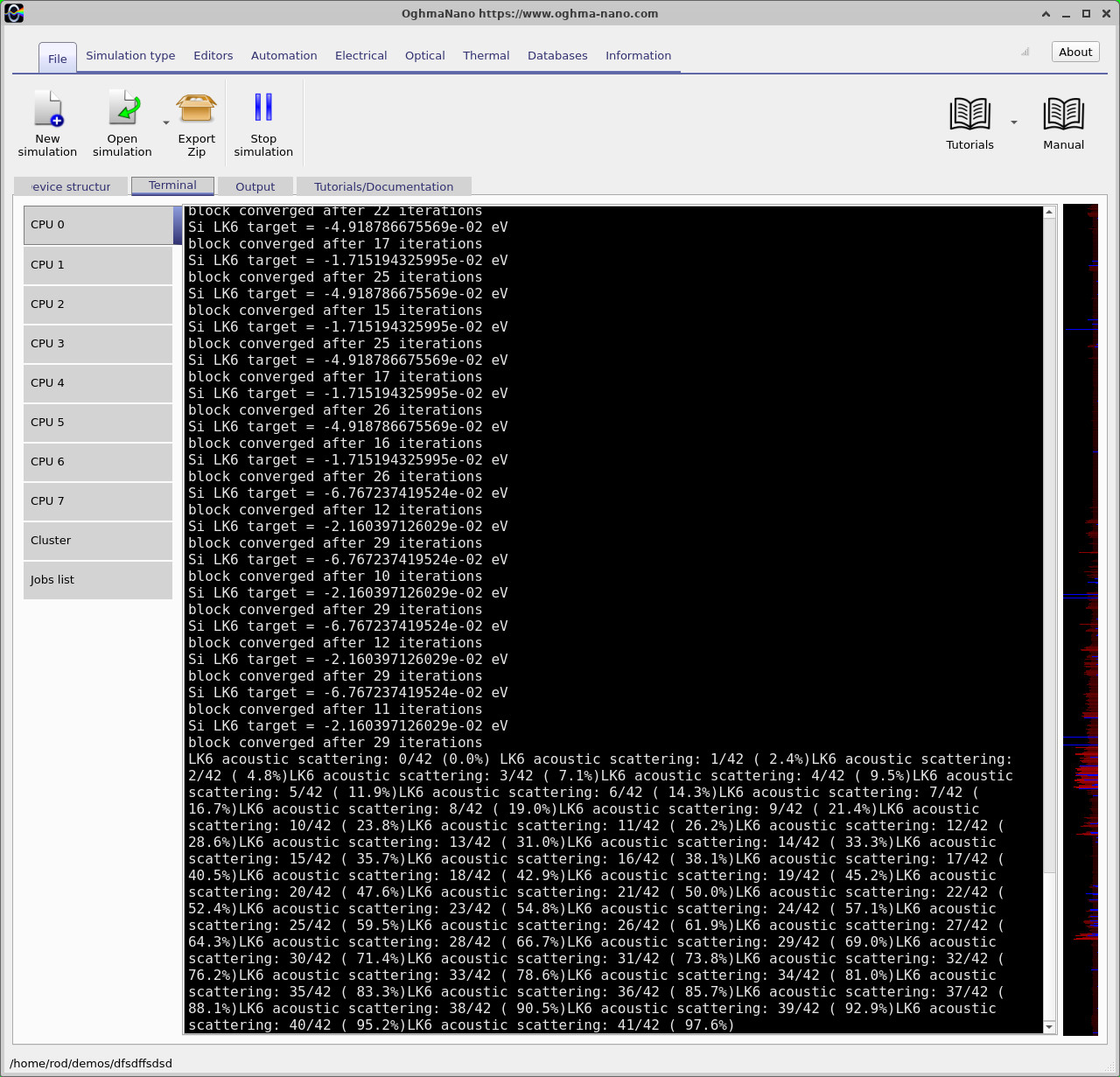
Wait for the solver to finish. Scattering takes additional time because transitions must be evaluated between occupied initial and available final electronic states, rather than finding the subband energies alone.
6. Reading the calculated valence-band dispersion
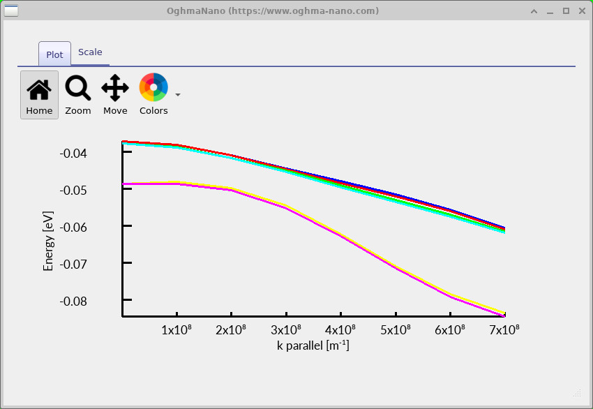
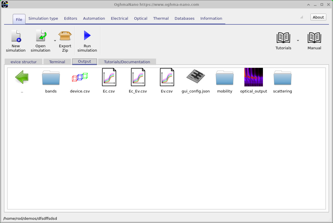
Open the Output tab. The resulting files include band-related plots as well as scattering and mobility folders (??). Open the valence-band result to obtain ??.
At \(k_{\parallel}=0\), confinement determines the discrete starting energy of each subband. Moving to finite \(k_{\parallel}\), the branches bend down in the displayed electron-energy convention, with somewhat different curvature and separation. The close pairs of lines are consistent with spin-related (Kramers) partners in a time-reversal-symmetric calculation; they should not automatically be assigned to different hole species.
A useful way to understand this plot is to remember that the hole is the absence of an electron in the valence band. Hole energy can therefore be expressed relative to a chosen valence-band reference as
\[ E_h(\mathbf{k}_{\parallel})=E_{v,\mathrm{ref}}-E_v(\mathbf{k}_{\parallel}). \]
Thus, a valence-electron branch curving downwards away from its maximum corresponds to an increasing hole excitation energy. The actual HH/LH/SO character of an individual branch is determined from the six-component eigenvector, not solely from its colour or curvature.
It is worth comparing this result with the conduction-band dispersion in the silicon Δ-valley tutorial. There the different valley orientations are treated using anisotropic electron masses; here the hole states are coupled directly in the multiband valence Hamiltonian.
7. Acoustic-phonon scattering and the hole lifetime
A band structure tells us which hole states are available, but it cannot by itself predict how quickly a hole loses its momentum. In this example OghmaNano uses the computed confined states to evaluate acoustic-phonon scattering. An acoustic phonon produces a small strain field in the crystal, perturbing the valence bands and potentially transferring a hole from an initial state \(i\) to a final state \(f\).
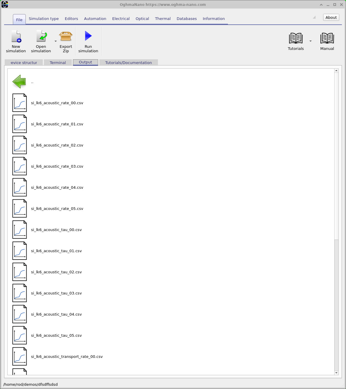
si_lk6_acoustic_rate_*.csv, si_lk6_acoustic_tau_*.csv and transport-related datasets.
Open the scattering folder in the Output tab
(??).
The numbered files represent the calculated states. For example, the provided screenshot of
si_lk6_acoustic_tau_02.csv plots the acoustic-scattering lifetime against
in-plane wavevector.
The physical starting point is Fermi's golden rule,
\[ W_{i\rightarrow f}=\frac{2\pi}{\hbar} \left|\langle\Psi_f|H_{\mathrm{e-ph}}|\Psi_i\rangle\right|^2 \delta(E_f-E_i\pm\hbar\omega_{\mathbf q}). \]
The matrix element describes how strongly a lattice vibration couples the two hole states; the delta function represents energy conservation for phonon absorption or emission. In a six-band valence model, the coupling depends on the multi-component hole wavefunctions, so the allowed transitions are influenced by HH/LH/SO mixing as well as the available final energies. The present output concerns the acoustic-phonon approximation used by this example.
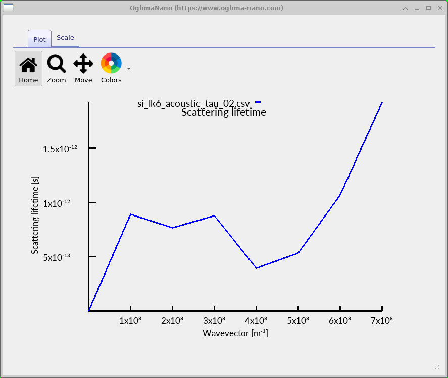
si_lk6_acoustic_tau_02.csv. Its variation with wavevector reflects the available final states and their coupling.Summing the allowed transitions gives the total event rate \(\Gamma_i\), with the corresponding lifetime
\[ \Gamma_i=\sum_f W_{i\rightarrow f},\qquad \tau_i=\frac{1}{\Gamma_i}\quad(\Gamma_i\gt 0). \]
The lifetime shown in ?? is not constant. It changes as the wavevector moves through different parts of the coupled valence dispersion. The zero displayed at the first sampled point should be treated as a boundary/output convention or a value requiring inspection, not as proof of a physically vanishing scattering lifetime at exactly \(k_{\parallel}=0\).
There is a further distinction important for transport: not every collision relaxes current equally. Small-angle scattering can change the microscopic state while having relatively little influence on the net direction of motion. A transport-weighted rate is therefore often written schematically as
\[ \Gamma_{\mathrm{tr},i}=\sum_f W_{i\rightarrow f} \left(1-\cos\theta_{if}\right),\qquad \tau_{\mathrm{tr},i}=\frac{1}{\Gamma_{\mathrm{tr},i}}. \]
The angular expression illustrates the momentum-relaxation principle; for anisotropic mixed bands, the full transport calculation must use the appropriate velocities and weighting. This is why the output separates acoustic-scattering rates/lifetimes from transport-related quantities rather than using a single number for every purpose.
8. From hole density and Fermi level to mobility
To obtain a measurable transport property we must combine the scattering information with how many holes occupy each part of each subband. The tutorial therefore includes a sweep of sheet hole density \(p_{2D}\), with units of m−2.
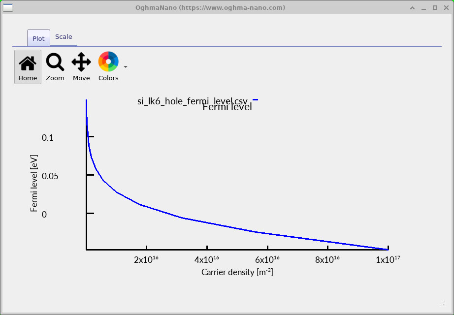
si_lk6_hole_fermi_level.csv as the sheet density is increased.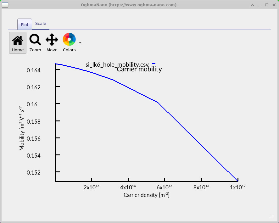
si_lk6_hole_mobility.csv across the same sheet-density sweep.The Fermi level specifies which electronic states are populated. For a valence-electron energy \(E_v\), the equilibrium occupation of the corresponding hole state can be written
\[ f_h(E_v)=1-f_e(E_v) =\frac{1}{1+\exp\!\left[(E_F-E_v)/(k_B T)\right]}. \]
Raising the sheet hole density shifts the chemical potential relative to the valence states, which is what the left-hand plot illustrates. The precise numerical energy values depend on the reference adopted by the model; the direction of the sweep and the resulting populations are the central features.
OghmaNano then weights the velocity and transport relaxation time of the populated states to obtain the in-plane sheet conductivity \(\sigma_{2D}\). The corresponding hole mobility is
\[ \mu_h=\frac{\sigma_{2D}}{q\,p_{2D}}, \qquad \sigma_{2D}\sim q^2\sum_n\int \frac{d^2 k_{\parallel}}{(2\pi)^2} \,v_{n,x}^{2}\,\tau_{\mathrm{tr},n} \left(-\frac{\partial f_e}{\partial E}\right). \]
Here \(v_{n,x}\) is the in-plane group velocity of subband \(n\), and the integral indicates that states at different wavevectors contribute differently to the current. The mobility plot (??) falls modestly over the displayed density range (roughly 0.165 to 0.151 m2 V−1 s−1). This is a result for the configured example and its included scattering physics, not a universal silicon hole-mobility law or a prediction incorporating every experimental loss mechanism.
9. Try it yourself
💡 Suggested experiments: Save a copy of the default example, then change only one quantity at a time.
- Change the Si well width from 10 nm and rerun the calculation. Compare the confined valence energies: a narrower well generally increases the scale of quantum confinement, although the mixed HH/LH/SO response is more complicated than a single-mass model.
- Compare hole and electron models: Run the companion silicon Δ-valley example with a comparable layer stack. Observe that the valence solver describes coupled six-component hole states, whereas the conduction calculation distinguishes silicon valley orientations.
- Inspect a second acoustic-lifetime file such as
si_lk6_acoustic_tau_00.csvand compare it withsi_lk6_acoustic_tau_02.csv. Different subbands need not have the same accessible scattering channels. - Inspect the density sweep: Compare the changes in Fermi level and mobility rather than assuming that a single effective lifetime predicts both curves.
This completes the six-model introductory quantum-well series. For the full mathematical formulation and the meaning of the material parameters, continue to the six-band Luttinger–Kohn theory chapter and the Bir–Pikus strain chapter.