

Silicon/SiGe Quantum Well: Six Δ-Valley and Electron Mobility Tutorial
1. Introduction
In the previous quantum-well examples we used direct-gap III–V semiconductors to calculate confined conduction and valence states and optical transitions. Silicon requires a rather different starting point. Its conduction-band minima are not at the centre of the Brillouin zone (Γ). Instead, bulk silicon has six equivalent conduction-band minima, or Δ valleys, arranged in opposite pairs along the three cubic crystal axes. Their different effective masses become particularly important when carriers are confined to a thin layer.
Here we will simulate a 10 nm silicon quantum well between two 20 nm SiGe layers. We will examine the electron subband dispersion and then follow the calculation further than in the optical tutorials: from acoustic phonon scattering to transport relaxation, electron sheet density, Fermi level and mobility. The emphasis is on electron transport, not direct optical gain; silicon is an indirect-gap semiconductor.
2. Opening the silicon Δ-valley example
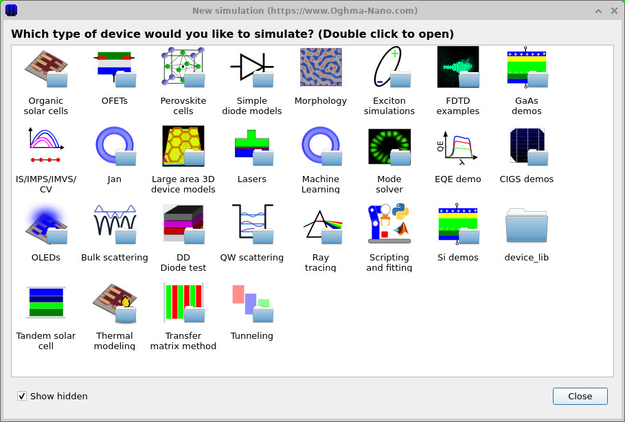
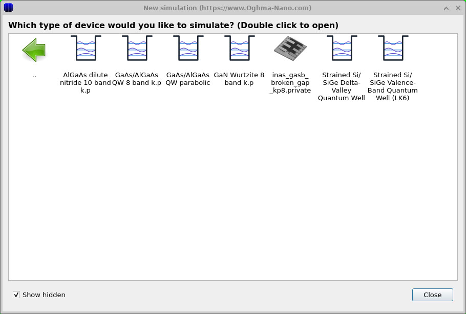
In OghmaNano select File → New simulation. Double-click the GaAs demos category in the template browser (??). This collection also contains the other semiconductor quantum-well models. In the next window, open Strained Si/SiGe Delta-Valley Quantum Well (??). Start with the supplied configuration unchanged so that your first run can be compared with the plots below.
3. Inspecting the Si/SiGe layer structure
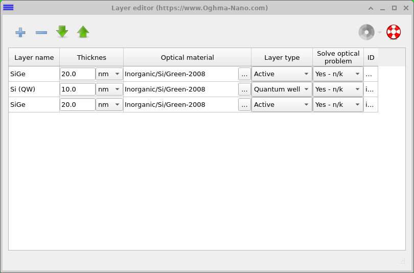
Click Layer editor in the device-structure panel to inspect the example (??). The confinement direction is through the three layers (taken as z here); electrons can still move parallel to the well in the x–y plane.
| Layer | Thickness | Layer type |
|---|---|---|
| SiGe | 20 nm | Active / barrier |
| Si (QW) | 10 nm | Quantum well |
| SiGe | 20 nm | Active / barrier |
The optical-material entries visible in the editor should not be mistaken for a complete specification of the electronic band offsets or Ge mole fraction. Those depend on the configured material parameters. Leave the supplied example as it is for now.
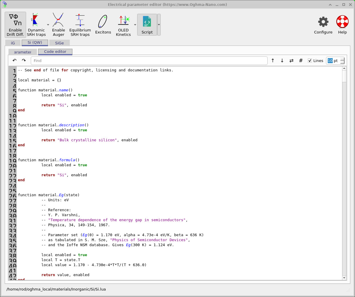
You can inspect the material data by opening Electrical parameters and selecting the Si (QW) tab (??). The silicon material library supplies temperature-dependent semiconductor parameters. For a predictive Si/SiGe calculation, the effective masses, band offsets, Ge composition and strain configuration are all worth checking, rather than relying on a bulk silicon band-gap value alone.
4. Why does silicon need a six-valley model?
Imagine an electron moving in the plane of the well. In an ordinary isotropic parabolic model, its energy depends only on the magnitude of its wavevector. Silicon is different: each Δ valley resembles an ellipsoid with a heavier longitudinal mass along its axis and a lighter transverse mass perpendicular to that axis. The valleys form the three opposite pairs ±x, ±y and ±z. Each pair is treated with the mass appropriate to its orientation relative to the quantum-well growth direction.
For a given valley, the effective-mass confinement problem can be written schematically as
\[ \left[-\frac{\hbar^2}{2}\frac{\partial}{\partial z} \left(\frac{1}{m_z^{*}(z)}\frac{\partial}{\partial z}\right) +V_{\Delta}(z)+\frac{\hbar^2 k_x^2}{2m_x^{*}(z)} +\frac{\hbar^2 k_y^2}{2m_y^{*}(z)}\right]\psi(z) =E(k_x,k_y)\psi(z). \]
Here \(V_{\Delta}\) is the conduction-band confinement potential for the chosen valley, including its strain-induced shift. The effective masses may vary from layer to layer. The important feature is that the mass along z controls confinement, while the two in-plane masses control the slope and curvature of the subband dispersion.
For a (001)-oriented well, the ±z pair (often called Δ2) has its longitudinal mass along the confinement direction. The four ±x/±y valleys (Δ4) instead have the transverse mass along z. Even without strain, their confinement energies need not coincide. Strain can further separate their valley edges, approximately according to
\[ \Delta E_{c,i}=\Xi_d\,\mathrm{Tr}(\varepsilon)+\Xi_u\,\varepsilon_{ii}, \qquad i\in\{x,y,z\}. \]
The first term shifts all valley orientations according to the overall dilation, whereas the second distinguishes the strain component along each valley's axis. This Δ2/Δ4 energy separation is not the same as the small interface-induced splitting between the two opposite valleys within one pair; the latter would require additional intervalley-coupling physics and should not be inferred from this plot alone. See the silicon Δ-valley theory page for more background.
5. Run the simulation
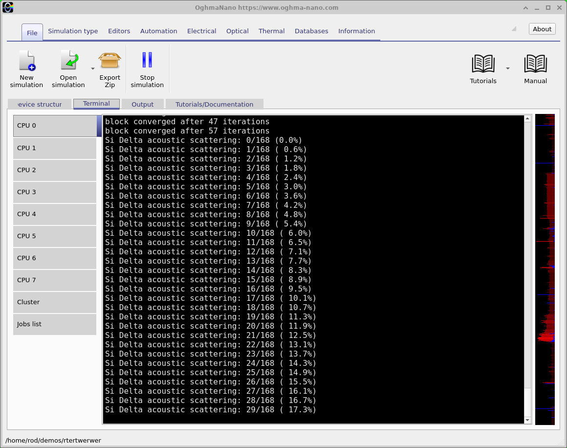
Return to the File ribbon and click Run simulation. The model solves the confined conduction states at a set of in-plane wavevectors before evaluating the electron scattering and transport results. In ??, the terminal has reached the acoustic-scattering stage. A percentage shown while the simulation is still running is a progress indicator, not a final scattering result.
Wait until the run completes, then use the Output tab to open the plots. In this tutorial we will look at the band dispersion first, followed by an individual wavevector-dependent scattering rate and the density-dependent transport quantities.
6. Reading the conduction-band dispersion
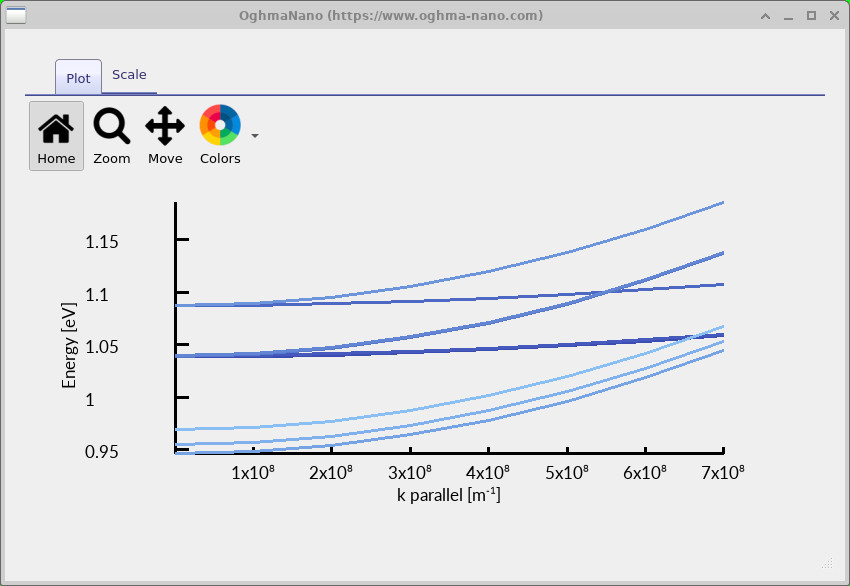
Open the conduction-band output to obtain ??. At zero in-plane wavevector each branch begins at a discrete confinement energy. As \(k_{\parallel}\) increases, the branches rise, but not all at the same rate. Some are substantially flatter because their effective in-plane mass is larger in the plotted direction. Close branches can approach or cross when they originate from separately treated valley orientations; one should not automatically interpret every proximity as a multiband anticrossing.
In a uniform-mass region, an individual oriented valley has the illustrative in-plane dispersion
\[ E_n(k_x,k_y)\simeq E_n(0)+\frac{\hbar^2 k_x^2}{2m_x^{*}} +\frac{\hbar^2 k_y^2}{2m_y^{*}}. \]
This is why it is useful to inspect the direction of the in-plane wavevector, rather than interpreting the set of coloured curves as copies of a single isotropic parabola. The plotted energy reference is the one used by the example; differences between the subband energies are usually more informative than their absolute offset.
7. From acoustic-phonon scattering to momentum relaxation
The band plot tells us which electron states are available. It does not, by itself, tell us how easily electrons can conduct along the well. To calculate mobility we must also ask how frequently phonons scatter an electron out of its current state, and—crucially—how effectively those events change its direction of motion.
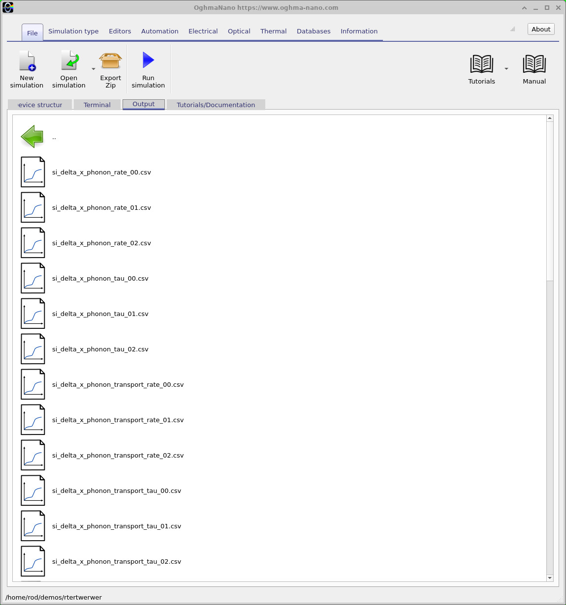
si_delta_x_phonon_rate_00.csv, the corresponding relaxation times (tau), and distinct transport_rate / transport_tau results. Other numbered files represent further calculated subbands.Open the scattering outputs in the Output tab (??). The example provides both ordinary phonon event rates and transport-weighted scattering rates. Their difference is not cosmetic: a collision through a very small angle changes an electron's state but may do little to relax its net momentum.
The starting point for a phonon transition is Fermi's golden rule, schematically
\[ W_{i\rightarrow f}=\frac{2\pi}{\hbar}|M_{fi}|^2 \,\delta(E_f-E_i\pm\hbar\omega_{\mathbf q}), \]
where the interaction matrix element \(M_{fi}\) contains the deformation-potential coupling and the overlap of the initial and final confined electron states. The sign allows phonon absorption or emission in the general case. For the acoustic calculation shown here, the usual near-elastic, thermal-phonon approximation is used. Longitudinal and transverse acoustic polarizations and the out-of-plane phonon wavevector are included in the confined-state calculation.
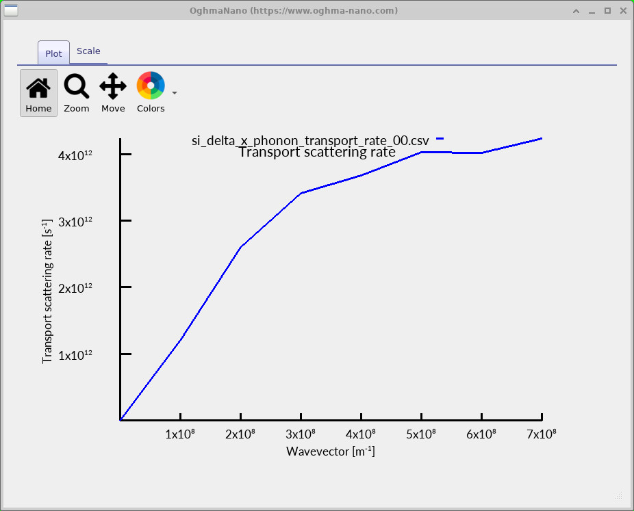
si_delta_x_phonon_transport_rate_00.csv, plotted for one of the silicon Δ-valley subbands.The transport rate introduces an additional angular weighting. For the simple momentum-direction picture used in this model, its role can be summarised as
\[ \frac{1}{\tau_{\mathrm{tr}}(i)} =\sum_f W_{i\rightarrow f}\bigl(1-\cos\theta_{if}\bigr), \qquad \tau_{\mathrm{tr}}=\frac{1}{\Gamma_{\mathrm{tr}}}. \]
Forward scattering (small \(\theta_{if}\)) is suppressed in this transport measure, whereas backscattering contributes more strongly. This is the reason a total phonon scattering lifetime and a transport lifetime need not be identical. The example transport-rate plot is shown in ??: the plotted rate generally increases with wavevector over the displayed range. Its precise shape depends on the subbands, allowed final states, material parameters and phonon overlaps.
The selected output is for the x-oriented valley family and one subband; it is not, on its own, the complete mobility of the six-valley electron gas. Nor should a zero or missing rate at exactly \(k=0\) in a sampled output be interpreted as proof that electrons there never scatter.
8. From Fermi level to mobility
Mobility is not evaluated at one arbitrarily selected wavevector. Electrons occupy a range of available states, and the occupied portion changes with sheet carrier density. The simulation therefore determines a Fermi level appropriate to the requested two-dimensional density and averages the transport response over the populated bands and valley orientations.
The Fermi–Dirac occupation of an electron state of energy \(E\) is
\[ f(E;E_F,T)=\frac{1}{1+\exp\!\left[(E-E_F)/(k_BT)\right]}. \]
Summing occupied states over the in-plane wavevectors and the relevant subbands provides a sheet density \(n_{2D}\) in m\(^{-2}\). Increasing \(n_{2D}\) typically requires raising the electron Fermi level: that progression appears directly in the first plot below.
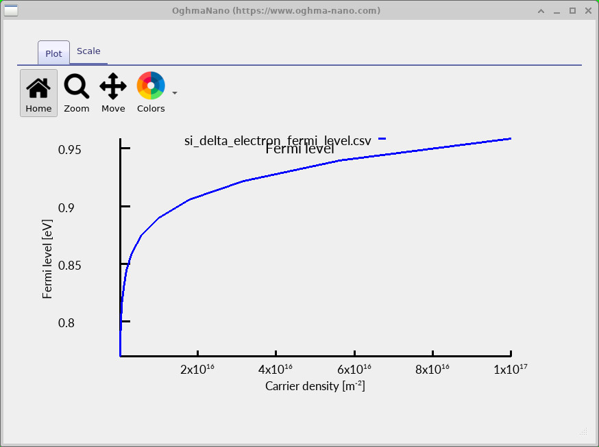
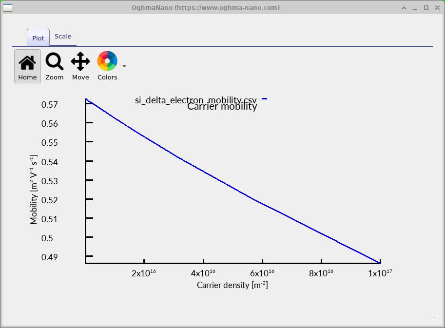
Under the transport relaxation-time treatment, the conductivity along the selected in-plane axis can be expressed in terms of the band velocities and the transport lifetimes:
\[ \sigma_{xx}^{2D}=e^2\sum_{n,v}\int\frac{d^2k_{\parallel}}{(2\pi)^2} v_{n,v,x}^2(\mathbf{k}_{\parallel})\, \tau_{n,v,\mathrm{tr}}(\mathbf{k}_{\parallel}) \left(-\frac{\partial f}{\partial E}\right), \qquad \mu_x=\frac{\sigma_{xx}^{2D}}{e\,n_{2D}}. \]
Here \(v_{n,v,x}\) is the electron group velocity along x for subband \(n\) of valley family \(v\). Appropriate valley multiplicities enter when summing the physically equivalent orientations. The factor \(-\partial f/\partial E\) gives most weight to states that can respond to a small applied field, rather than weighting every occupied state equally.
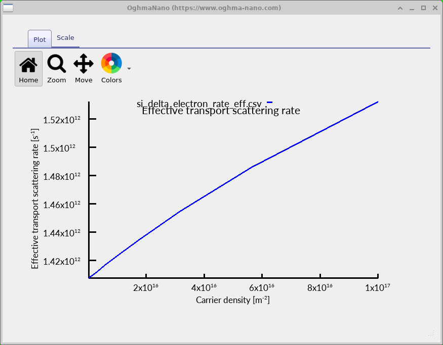
The computed mobility decreases from approximately 0.57 to 0.49 m2 V−1 s−1 over the displayed density range in ??. At the same time, the effective transport scattering rate rises, as illustrated in ??. This is consistent with the density-dependent occupation giving more weight to electron states with stronger momentum relaxation in this particular setup. The corresponding effective lifetime is a transport-weighted quantity and its inverse should not be confused with a separately plotted single-state phonon rate.
This example demonstrates the mobility predicted by the configured scattering model; it should not automatically be interpreted as a complete experimental Si/SiGe mobility including every possible disorder, interface, impurity and phonon mechanism.
9. Try it yourself
Once you can reproduce the supplied results, make one change at a time and rerun the calculation. The following experiments help connect the model inputs to the underlying physics:
💡 Suggested experiments
- Change the Si well width. Compare the lowest subband energies and examine how the different confinement masses affect the Δ-valley families.
- Inspect the strain and SiGe composition. Compare the valley energy offsets before and after the change; the Δ2 and Δ4 groups need not move together.
- Compare event and transport rates. Open the matching
phonon_rateandphonon_transport_ratefiles for the same valley and subband. They measure different things. - Change the target sheet density. Compare the Fermi-level, effective transport-rate and mobility plots, keeping the phonon and material parameters fixed.
The key result is that silicon mobility is connected to a chain of calculations: valley orientation and strain → confined subbands → available phonon transitions → transport lifetimes → occupied-state conductivity → mobility. This is the main difference between this example and the optical quantum-well tutorials.
📘 For the underlying band theory, continue to the six-valley silicon conduction-band model. The separate six-band Luttinger–Kohn model deals with confined silicon valence states rather than the Δ conduction valleys used here.