

GaAs/AlGaAs Quantum Well: 8-Band Zincblende k·p Tutorial
1. Introduction
In this tutorial we will calculate the electronic and optical properties of a GaAs/AlGaAs quantum well using OghmaNano's eight-band zincblende k·p model. We will begin with a ready-made example, inspect the layer structure, run the simulation and examine the resulting conduction and valence subbands. Finally, we will look at the optical spectra calculated from the states.
The parabolic quantum-well tutorial treats electrons and holes using comparatively simple effective-mass bands. Here, the Hamiltonian includes a conduction-band basis and the heavy-hole (HH), light-hole (LH) and split-off (SO) valence-band basis, with two spin components for each: eight basis states in total. The coupling between these states lets the model describe effects that independent parabolas cannot, particularly valence-band mixing and changes in curvature with in-plane wavevector.
2. Opening the eight-band example
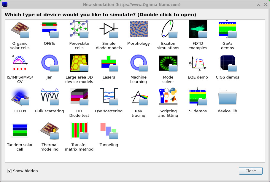
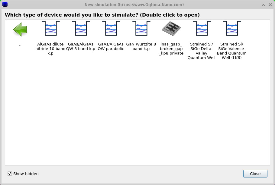
In OghmaNano, press New simulation on the File ribbon. Double-click the GaAs demos folder (??). From the quantum-well examples, double-click GaAs/AlGaAs QW 8 band k.p (??). This opens a preconfigured simulation; there is no need to enter an eight-by-eight Hamiltonian manually.
3. Quantum-well structure and material parameters
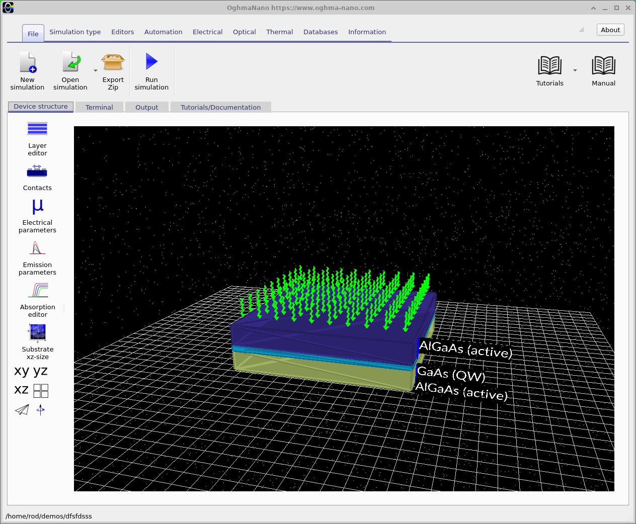
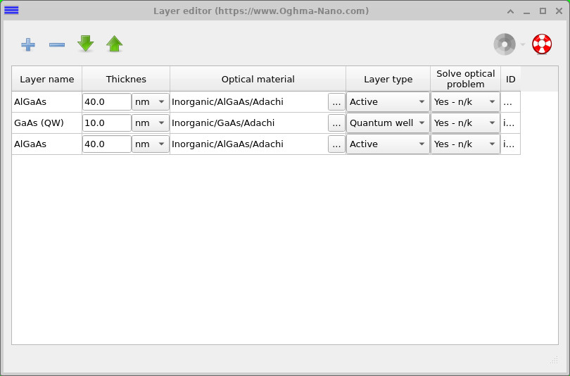
The main window displays a three-layer AlGaAs/GaAs/AlGaAs structure (??). Open the Layer editor using the button on the left. The supplied example consists of two 40 nm AlGaAs barriers surrounding a 10 nm GaAs well:
| Layer | Thickness | Layer type |
|---|---|---|
| AlGaAs | 40 nm | Active barrier |
| GaAs (QW) | 10 nm | Quantum well |
| AlGaAs | 40 nm | Active barrier |
The GaAs band edges lie within the surrounding AlGaAs band gap, providing confinement along the layer-growth direction. In the layer editor the central GaAs layer is marked specifically as Quantum well (??). The optical material entries and layer types are already configured in this example.
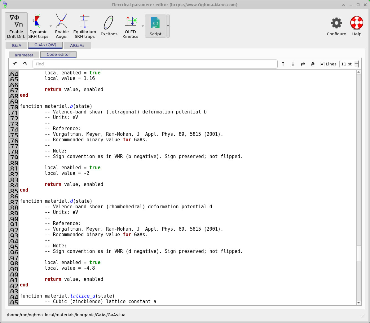
The eight-band solver needs more material information than a scalar parabolic-band
model: besides band edges and effective masses, parameters describing interband
coupling, the split-off energy and (where applicable) strain enter the Hamiltonian.
You can inspect the GaAs functions via Electrical parameters and the
material's Code editor
(??).
The screenshot shows the valence-band deformation potentials b and
d; you do not need to modify these for this introductory run.
What changes in the eight-band calculation?
A parabolic model assigns a separate curvature to each band. The k·p approach instead constructs a matrix whose off-diagonal elements couple the underlying basis states. Schematically, the confined-state problem is
\[ H_{8\times8}(k_x,k_y,-i\partial_z)\,\Psi_n(z) =E_n(k_x,k_y)\,\Psi_n(z). \]
Here \(z\) is the confinement direction; \(k_x\) and \(k_y\) describe motion parallel to the layers. The envelope wavefunction \(\Psi_n\) has eight components, which describe the contributions of the different basis states. For this tutorial we will concentrate on the calculated energies rather than the full matrix algebra. A detailed explanation is available in the eight-band zincblende theory chapter.
4. Running the simulation
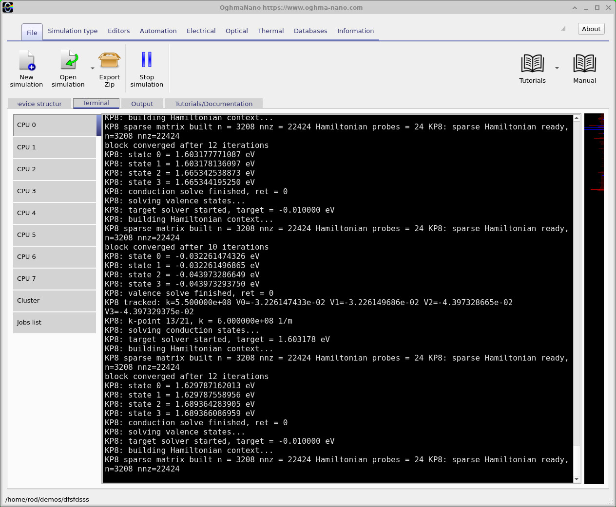
Return to the File ribbon and click the blue Run simulation button. The eight-band Hamiltonian is assembled and solved at a sequence of in-plane wavevectors. You can follow the calculation on the Terminal tab (??).
The example terminal shows the sparse matrix being built, followed by eigenstate
energies and messages such as block converged after 12 iterations.
Conduction and valence states are solved separately at successive wavevectors. Wait
until the run completes and the button returns to Run simulation
before inspecting the outputs.
5. Understanding the calculated band structure
The solver calculates a discrete set of confined eigenstates at each in-plane
wavevector \(k_{\parallel}\). The plot therefore shows subband dispersion,
rather than the spatial band-edge profile across the layers. Open the Output
tab and look in the bands folder, or open the summary band files displayed
in ??.
5.1 Conduction subbands
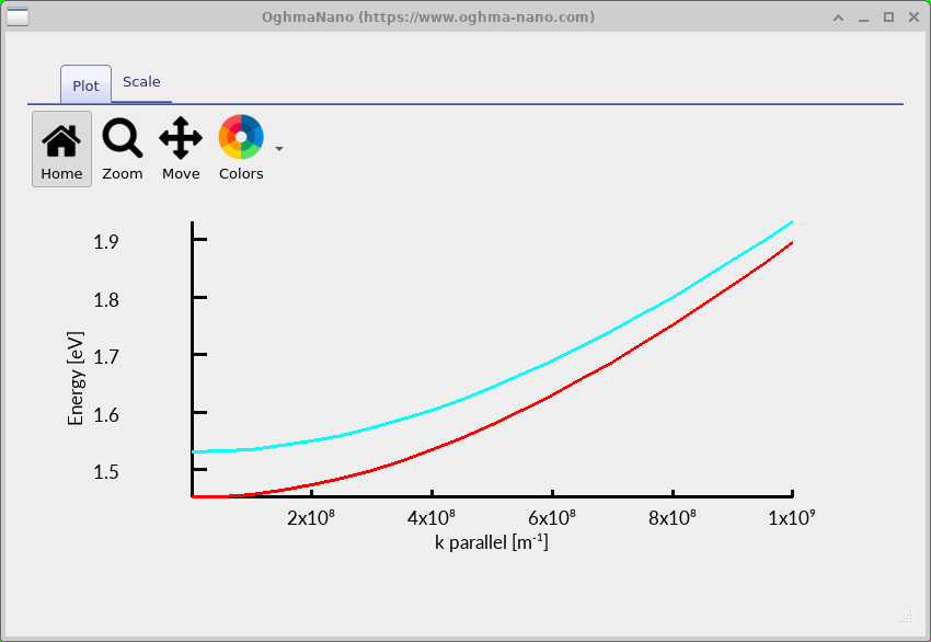
The conduction-band plot (??) displays two upwards-curving branches. At \(k_{\parallel}=0\), the vertical separation originates from the different confined states. The increasing energy with \(k_{\parallel}\) reflects motion parallel to the well, where the carriers are not confined.
Close to a conduction-subband minimum, the dispersion may be approximated by
\[ E_n(k_{\parallel})\simeq E_n(0) +\frac{\hbar^2 k_{\parallel}^{2}}{2m_{n,\parallel}^{*}}. \]
In the multiband model this is a local approximation: the curvature, and hence the apparent effective mass, need not remain constant over the whole plotted wavevector range. The conduction–valence coupling contributes to the behaviour.
5.2 Valence subbands: mixing and curvature
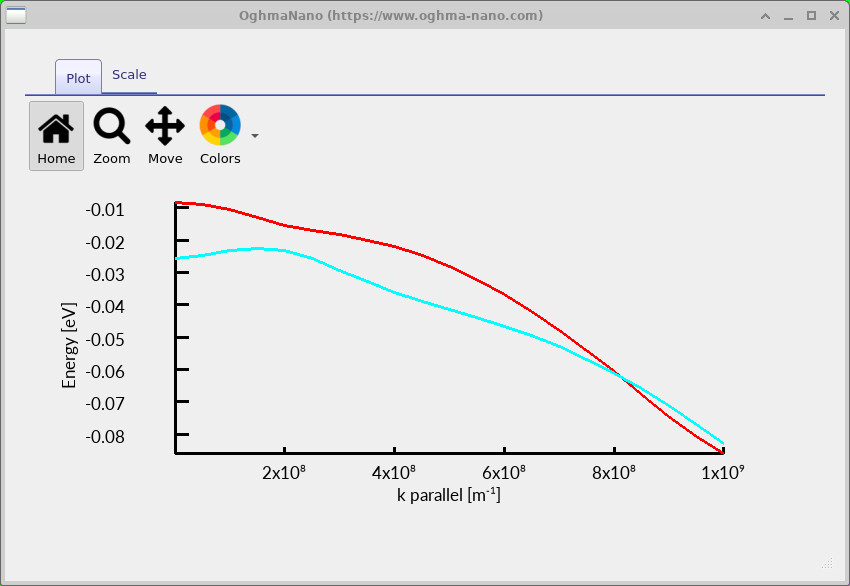
The valence-band plot is more interesting (??). Its two displayed branches start at different energies, curve downwards, and appear to meet at a finite value of \(k_{\parallel}\). In the zincblende valence band, the heavy-hole and light-hole states do not behave like two completely independent parabolas: at finite wavevector, terms in the Hamiltonian can mix their character.
A useful way of expressing this is to consider two nearby states, coupled by a matrix element \(V\):
\[ H_{\mathrm{illustrative}}= \begin{pmatrix}E_{\mathrm{HH}}(k)&V(k)\\ V^{*}(k)&E_{\mathrm{LH}}(k)\end{pmatrix}. \]
If they are allowed to couple, their energies repel near an encounter, and their HH/LH character can exchange between branches. A genuine crossing is also possible where the relevant coupling vanishes by symmetry. The present screenshot alone does not distinguish these cases: to establish the state character, inspect the corresponding eigenvectors and, if needed, calculate more points near the apparent intersection. The two-by-two matrix above is just an illustration, not the full eight-band Hamiltonian.
5.3 Viewing conduction and valence states together
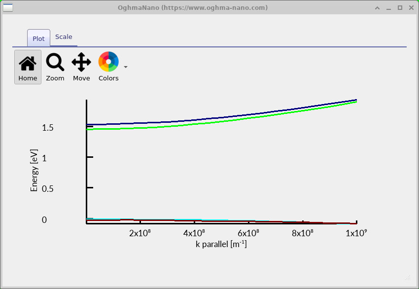
The combined plot (??) places the electron and valence-electron states on a common energy scale. In this example, the valence states sit near the energy reference, while the confined conduction states lie around 1.5 eV and above. The gap between a given pair of states is the photon energy of a possible vertical optical transition, subject to the relevant optical matrix element and carrier occupations.
Because photon momentum is comparatively small, the useful first approximation is that an optical transition preserves in-plane wavevector:
\[ \hbar\omega=E_{c,n}(k_{\parallel})-E_{v,m}(k_{\parallel}), \qquad \lambda=\frac{hc}{\hbar\omega}. \]
Different pairs of electron and hole states therefore contribute at different wavelengths. The multiband wavefunctions also determine the strength and polarisation of each transition, beyond what can be read from energies alone.
6. Optical properties of the quantum well
The eight-band calculation supplies electronic energies and mixed-state wavefunctions for the optical model. The example produces separate spectra for stimulated emission, absorption, net gain and spontaneous emission. The multiple curves in each plot correspond to the sequence of carrier conditions used by the supplied simulation; they are not eight individual Hamiltonian bands.
6.1 Stimulated emission and absorption
Stimulated emission occurs when an incoming photon induces an electron to make a radiative transition from a filled conduction state to an empty valence state. Absorption is the reverse process: a valence electron takes up a photon and moves into an available conduction state. Their occupation factors are, schematically,
\[ \begin{aligned} \text{stimulated emission:}&\quad f_c(1-f_v),\\ \text{absorption:}&\quad f_v(1-f_c). \end{aligned} \]
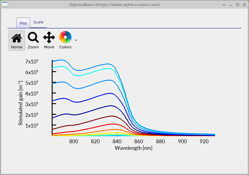
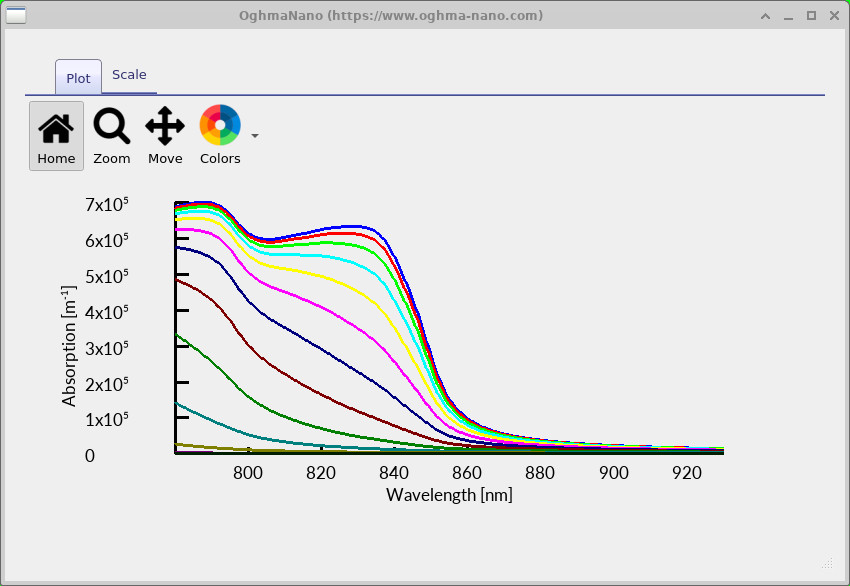
The stimulated-emission curves (??) and absorption curves (??) share their underlying transition energies, but their strengths differ as the occupations change. In these results, much of the spectral structure lies around 790–850 nm; the exact features depend on the configured subbands, matrix elements, carrier populations and line broadening.
6.2 Net gain: when emission exceeds absorption
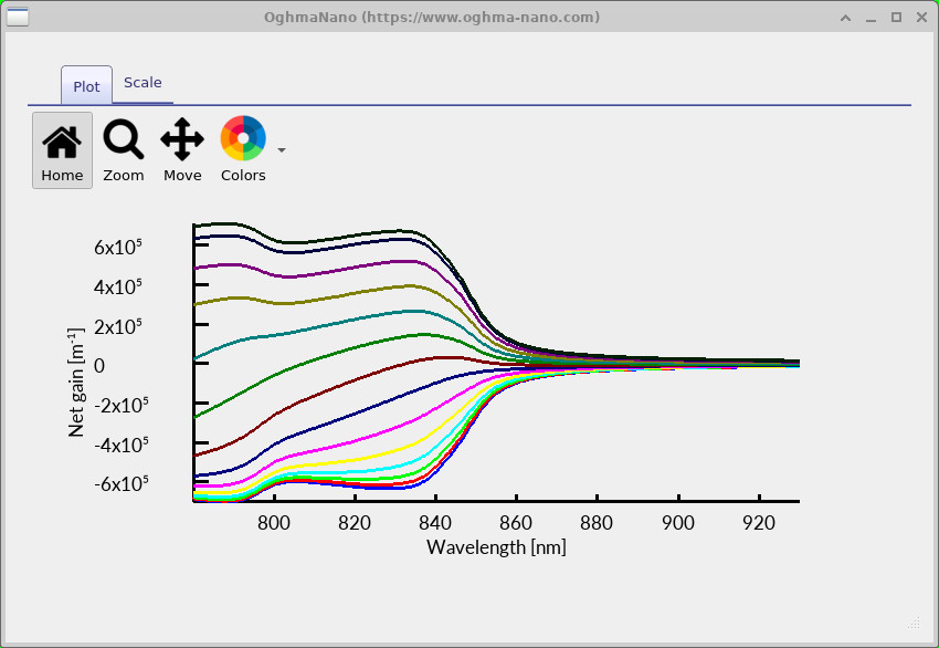
The net gain plot (??) combines the competing stimulated emission and absorption contributions. Subtracting their occupation probabilities gives a particularly simple result:
\[ f_c(1-f_v)-f_v(1-f_c)=f_c-f_v. \]
Thus the transition becomes gain-producing when its participating conduction state is more occupied than the corresponding valence electron state. Negative net-gain values represent absorption-dominated conditions; positive values correspond to stimulated emission exceeding absorption. The net-gain coefficient shown here is the quantum-well optical result; it should not automatically be interpreted as the modal gain of a complete laser cavity, which also depends on confinement and other optical losses.
6.3 Spontaneous emission
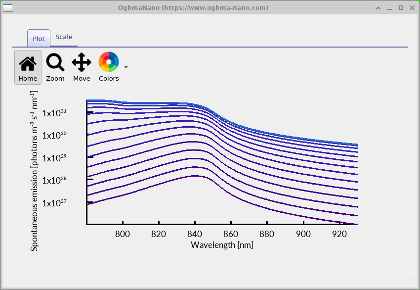
Spontaneous emission does not require an incident photon to trigger the transition. It occurs when an occupied electron state recombines radiatively into an available valence state. The corresponding occupation factor is again \(f_c(1-f_v)\), but spontaneous and stimulated emission have different spectral prefactors and physical interpretations. The spectra in ?? use a logarithmic vertical scale; equal vertical spacing therefore does not mean equal absolute increases in the emitted photon rate.
For a fuller explanation of transition strengths, carrier occupations and line broadening, see the optical transitions and gain theory pages.
7. Finding the output files
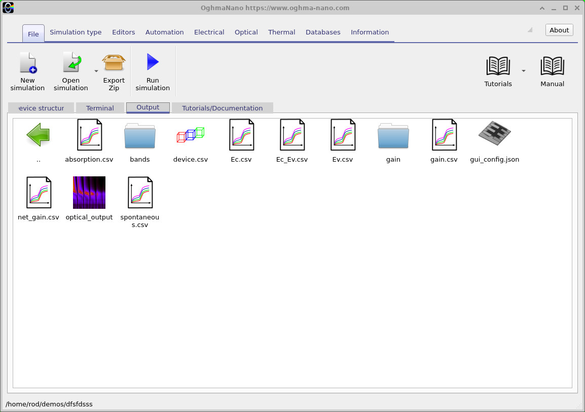
bands and gain directories contain additional results.
After the simulation finishes, select Output in the main window
(??).
Among the visible results are Ec.csv, Ev.csv and
Ec_Ev.csv for the band plots, together with gain.csv,
absorption.csv, net_gain.csv and
spontaneous.csv. The bands and gain
folders contain further solver outputs. Double-click a CSV file to open its plot
in OghmaNano, or export the numerical data for analysis elsewhere.
8. Try it yourself: compare against the parabolic model
Suggested experiment: Run the parabolic GaAs/AlGaAs example alongside this eight-band calculation, keeping the GaAs well width at 10 nm and checking that the materials and other settings are comparable. Compare the resulting band plots and optical spectra.
- Are the lowest conduction subbands approximately parabolic near \(k_{\parallel}=0\)?
- How does the valence-band dispersion differ from the independent parabolic picture?
- How do the calculated optical thresholds and relative spectral features change?
As a second experiment, change the GaAs well thickness from 10 nm to 8 nm while keeping both 40 nm AlGaAs barriers unchanged. Re-run the model and compare the confined eigenenergies and the wavelength range of the optical transitions.
✅ What to look for
Close to a band extremum, an eight-band result can resemble an effective-mass parabola. Further from the extremum, mixing and non-parabolicity become easier to see, especially for valence states. A narrower well generally increases confinement energies and shifts the low-energy interband transitions towards higher photon energy (shorter wavelength); the precise change depends on the material parameters and coupled eigenstates.
📘 Continue with the eight-band zincblende k·p theory to understand the basis states and Hamiltonian, or the optical transitions chapter for the connection between these subbands and the spectra.