

GaAs/AlGaAs Parabolic Quantum Well Tutorial
1. Introduction
In this tutorial we will calculate the electronic and optical properties of a simple GaAs/AlGaAs quantum well using the parabolic-band model in OghmaNano. A thin GaAs layer is placed between two wider-band-gap AlGaAs barriers. The change in band-edge energy confines electrons and holes in the growth direction, while they remain free to move parallel to the layers. This produces discrete confinement energies which develop into two-dimensional electronic subbands.
We will start from a ready-made simulation, inspect the layer structure, run the model, and look at its calculated conduction and valence subbands. We will then examine how those states contribute to absorption, stimulated emission, net optical gain and spontaneous emission. If you are new to the physics, the parabolic-band theory page gives a more detailed introduction.
2. Opening the quantum-well example
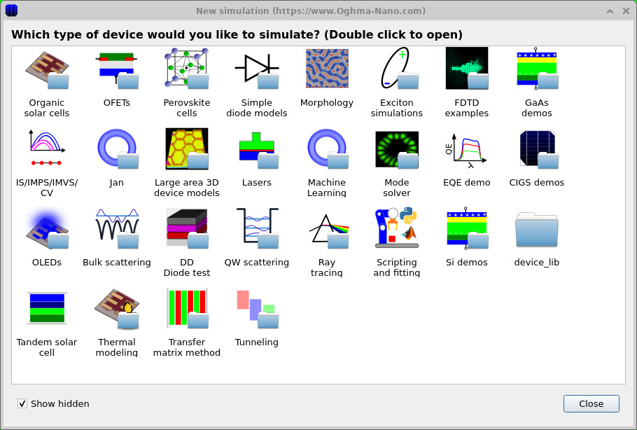
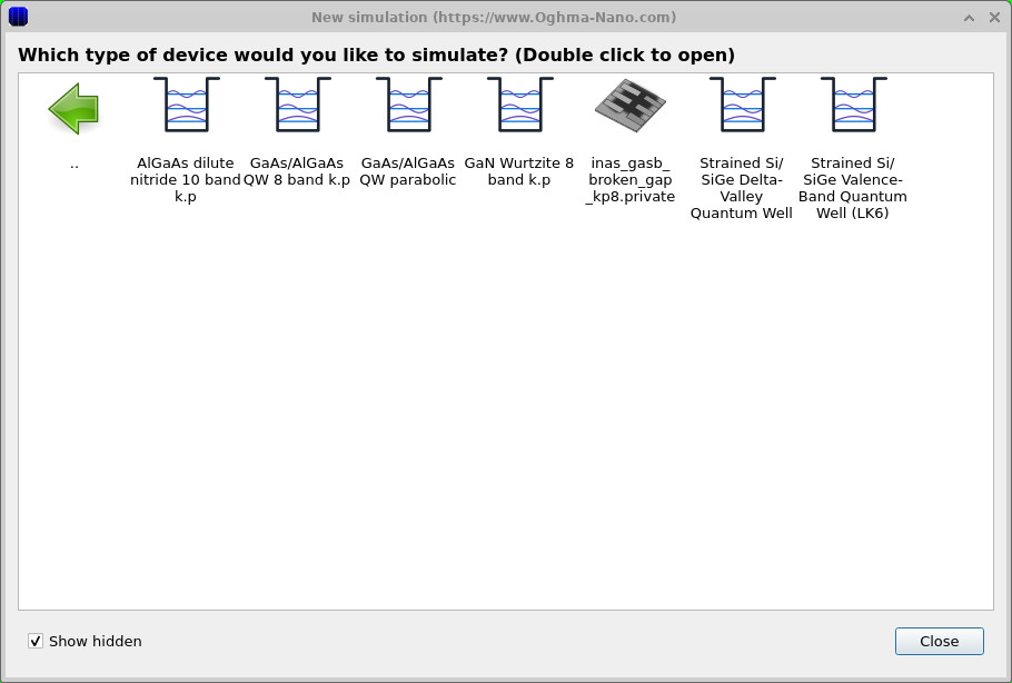
Open OghmaNano and select New simulation from the File ribbon. In the device chooser, double-click GaAs demos (??). This opens the selection of semiconductor and quantum-well examples. Double-click GaAs/AlGaAs QW parabolic (??). The preconfigured example will open in the main simulation window.
3. Understanding the device structure
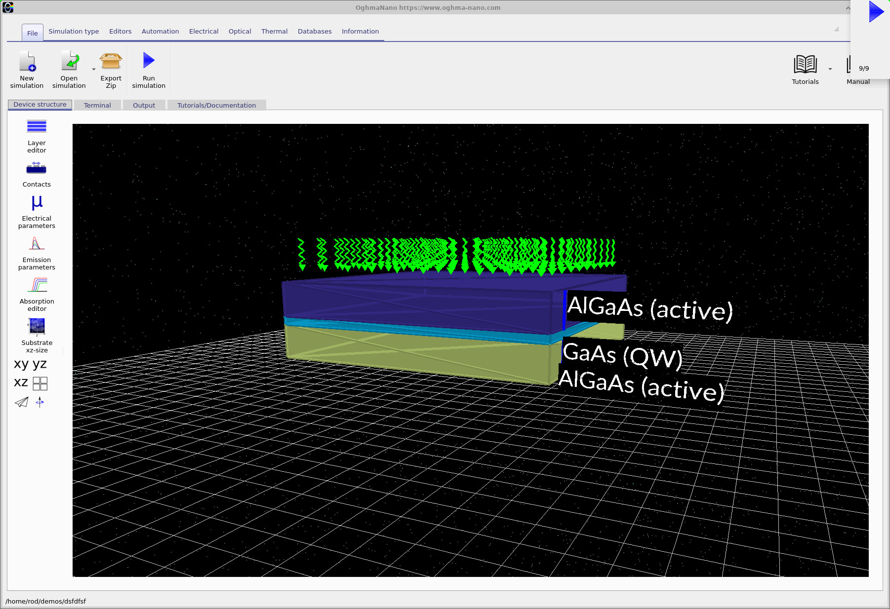
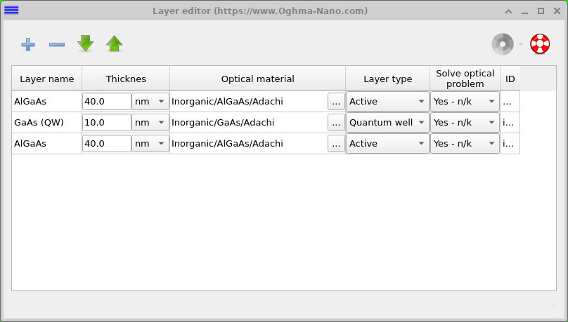
The main window displays the three-layer structure (??). The GaAs layer is the well; the two surrounding AlGaAs layers provide the barriers. Click Layer editor on the left of the main window to inspect the dimensions. The supplied example uses the following structure:
| Layer | Thickness | Purpose |
|---|---|---|
| AlGaAs | 40 nm | First barrier |
| GaAs (QW) | 10 nm | Quantum well |
| AlGaAs | 40 nm | Second barrier |
Notice that the centre layer is explicitly assigned the Quantum well layer type, rather than Active. The entries and optical material selections are visible in ??. The wider-band-gap barriers create the confinement potentials; the exact band offsets depend on the material parameters used in the example.
Why does changing the well width matter?
Confinement along the growth direction permits only particular electron and hole wavefunctions. In the simplest idealisation of a one-dimensional infinite well of width \(L\), the electron confinement energies, measured from the bottom of the well, are
\[ E_n=\frac{n^2\pi^2\hbar^2}{2m^{*}L^2},\qquad n=1,2,3,\ldots \]
Here \(m^{*}\) is the carrier effective mass and \(\hbar\) is the reduced Planck constant. The real example has finite AlGaAs barriers, so OghmaNano solves for the confined states using its actual material profile rather than assuming this infinite-well expression. Nevertheless, the equation gives a useful prediction: reducing the GaAs well width generally raises the electron confinement energies. Holes have their own effective mass and corresponding confinement energies.
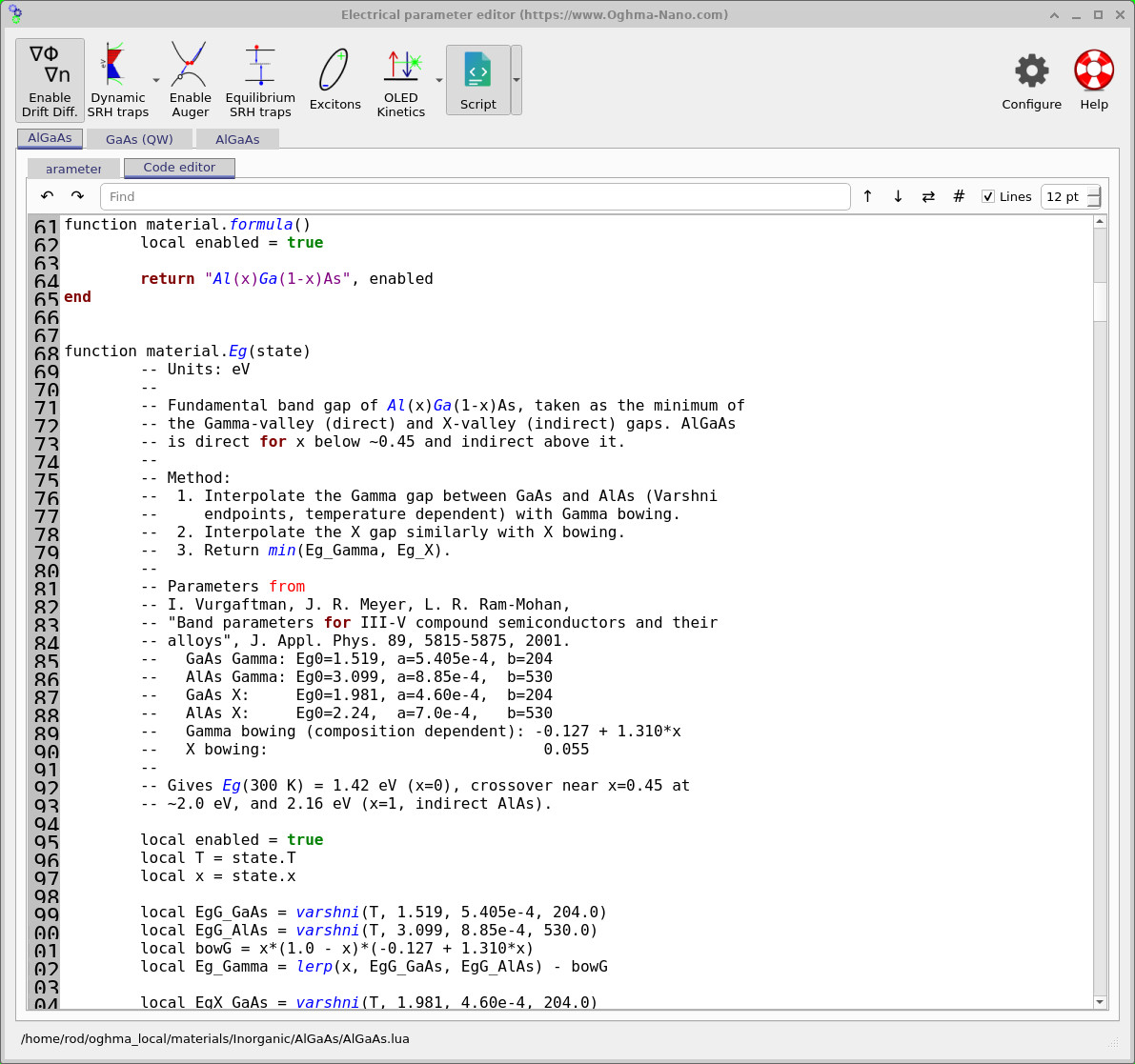
You can examine or edit the underlying material functions through the Electrical parameters button. In the screenshot, the AlGaAs material definition includes a composition- and temperature-dependent band-gap calculation (??). You do not need to edit the material code to complete this introductory tutorial.
4. Running the simulation
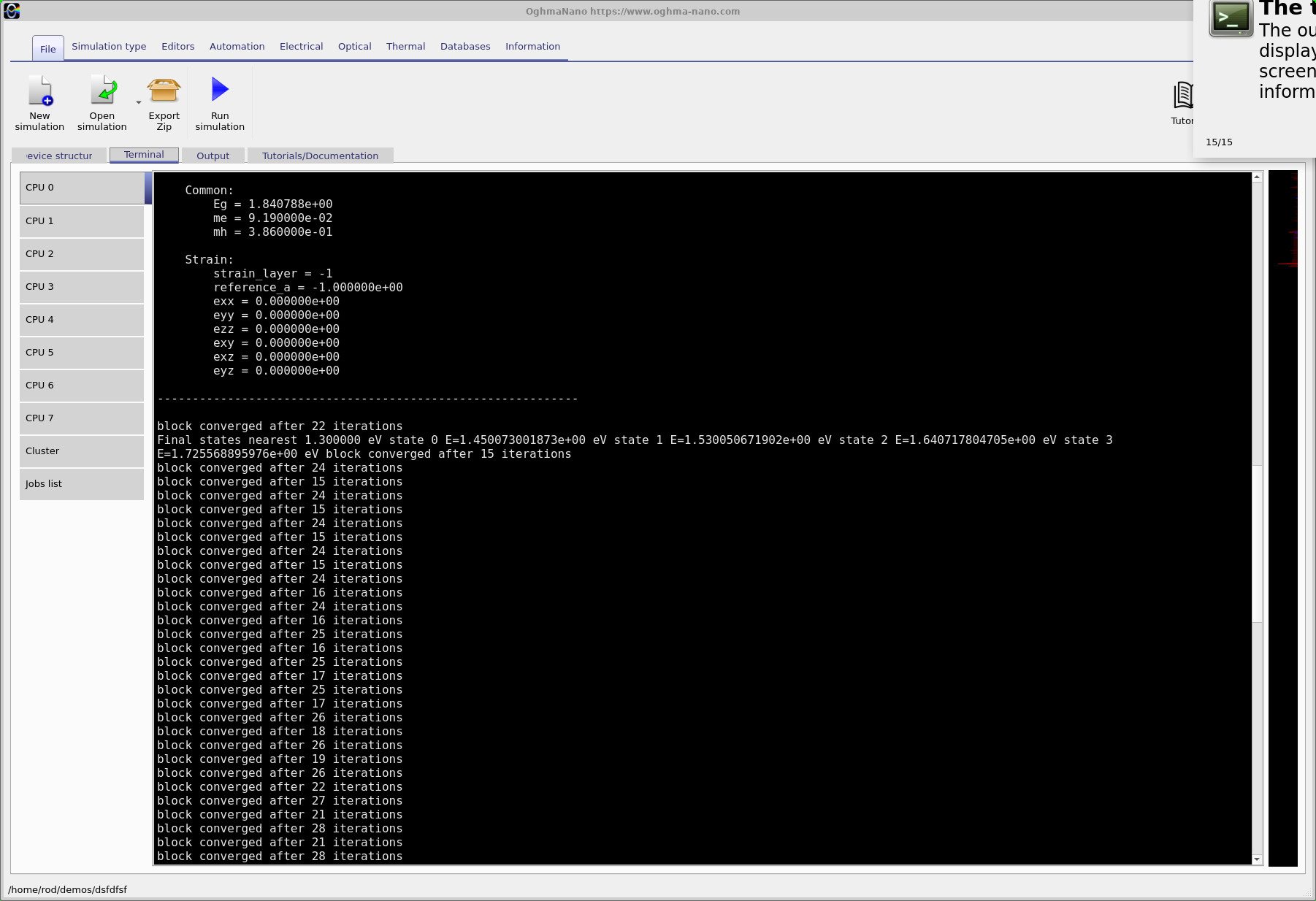
Return to the File ribbon and press Run simulation (the blue
triangular button). The Terminal tab displays messages from the solver as it runs.
In the supplied example, the terminal reports eigenstate energies and repeated
block converged after ... iterations messages
(??).
Wait for the run to finish before opening the plots.
The solver calculates the quantised states across the layers and then examines their variation with in-plane wavevector, \(k_{\parallel}\). Where the optical calculation is configured, it also generates spectra for the different carrier conditions in the example.
5. Electronic subbands: interpreting the band plot
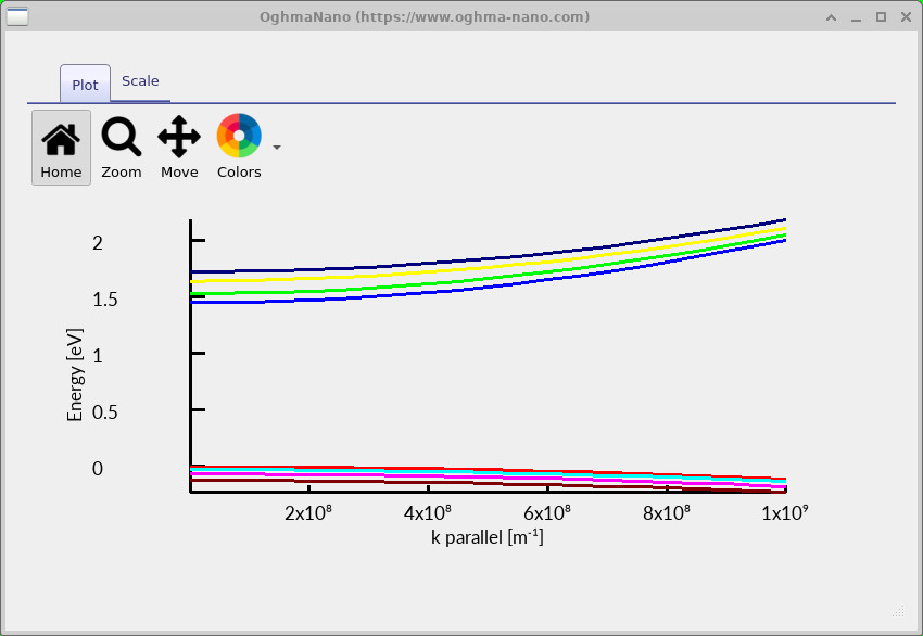
Open the calculated band-dispersion plot (??). There are two visibly distinct groups of curves: the conduction subbands at positive energies and the valence subbands close to and below the valence-band reference. The vertical separation reflects the semiconductor band gap together with the confined electron and hole energies. The different starting energies within each group arise from the quantised states of the well.
Although the motion across the well is confined, carriers can still move along the layers. This is why a single confined energy becomes a parabola when plotted against the parallel wavevector:
\[ E_{e,n}(k_{\parallel})=E_{e,n}(0) +\frac{\hbar^2 k_{\parallel}^2}{2m_e^{*}}. \]
Here \(E_{e,n}(0)\) is the energy at the bottom of electron subband \(n\). For the corresponding valence-electron subbands, the simple parabolic form bends downwards:
\[ E_{v,m}(k_{\parallel})=E_{v,m}(0) -\frac{\hbar^2 k_{\parallel}^2}{2m_h^{*}}. \]
This is the defining approximation of the tutorial: the states have quantised energies in the confinement direction but retain an effective-mass dispersion in the plane. More advanced multiband k·p models allow the bands to mix and become non-parabolic; the 8-band zincblende theory page explains why that can matter.
6. From the subbands to optical spectra
Electrons can undergo optical transitions between valence and conduction subbands. At normal optical incidence the photon momentum is small compared with the electronic wavevector, so a simple model considers transitions that conserve the in-plane wavevector. At the centre of the dispersion, the approximate photon energy for a transition between confined electron level \(n\) and hole level \(m\) is
\[ \hbar\omega\simeq E_g+E_{e,n}^{\mathrm{conf}}+E_{h,m}^{\mathrm{conf}}. \]
The two confinement energies are measured upward from their respective well band edges. The available transitions, the occupation of their initial and final states, and any spectral broadening determine the shape of the calculated optical response. You can explore these ideas further on the optical transitions theory page.
6.1 Stimulated emission and net gain
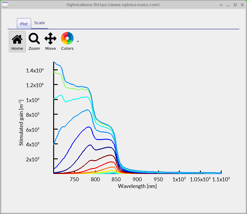
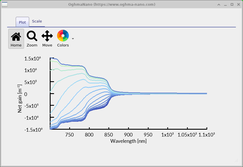
The stimulated-emission plot (??) shows the calculated emission contribution as a function of wavelength for the series of carrier conditions used in the example. The distinct spectral steps and shoulders are associated with the energies at which different subband transitions contribute. The separate net gain output (??) includes the competing stimulated absorption contribution and can therefore be positive or negative.
Schematically, for a conduction state occupied with probability \(f_c\) and a valence electron state occupied with probability \(f_v\), the net stimulated contribution contains the occupation factor
\[ \underbrace{f_c(1-f_v)}_{\text{stimulated emission}} -\underbrace{f_v(1-f_c)}_{\text{absorption}} =f_c-f_v. \]
A positive net stimulated contribution requires sufficient inversion of the states participating in the transition. The total plotted spectrum additionally depends on the optical transition strengths and the number of available states.
6.2 Absorption and spontaneous emission
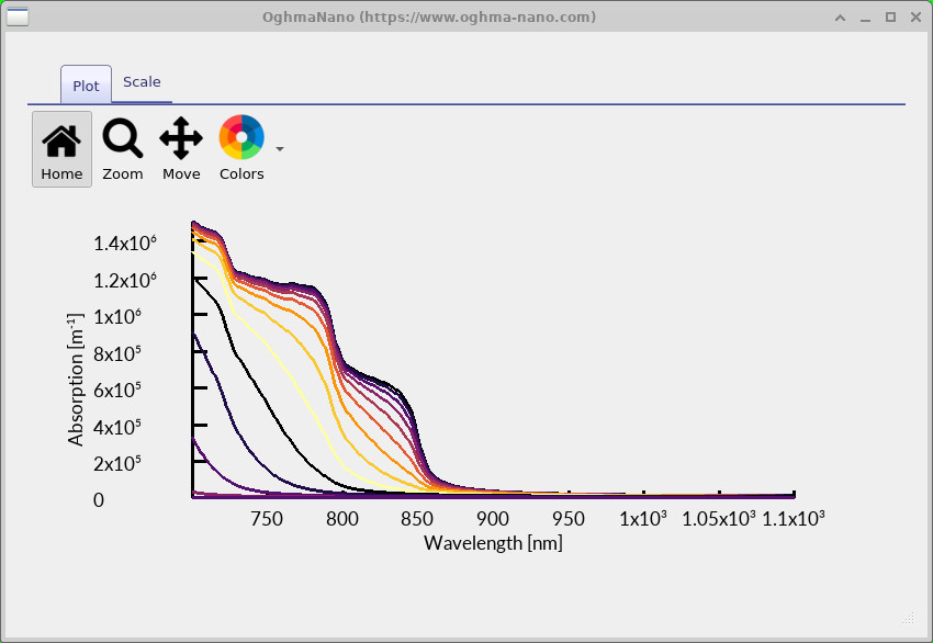
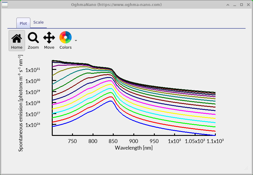
The absorption plot (??) records the absorption contribution of the allowed transitions. Absorption requires an occupied initial valence state and an available final conduction state. The spontaneous-emission plot (??) represents radiative recombination of occupied conduction states into empty valence states without requiring an incident photon to stimulate the transition. Accordingly, the spontaneous-emission occupation factor contains \(f_c(1-f_v)\).
Notice that the pronounced spectral features occur in similar wavelength regions across these plots. That is expected: the same underlying electron and hole subband structure supplies the possible optical transition energies, while carrier occupations distinguish absorption from the different types of emission. The spontaneous-emission plot uses a logarithmic vertical scale, so take care when comparing curve heights.
7. Finding the calculated files
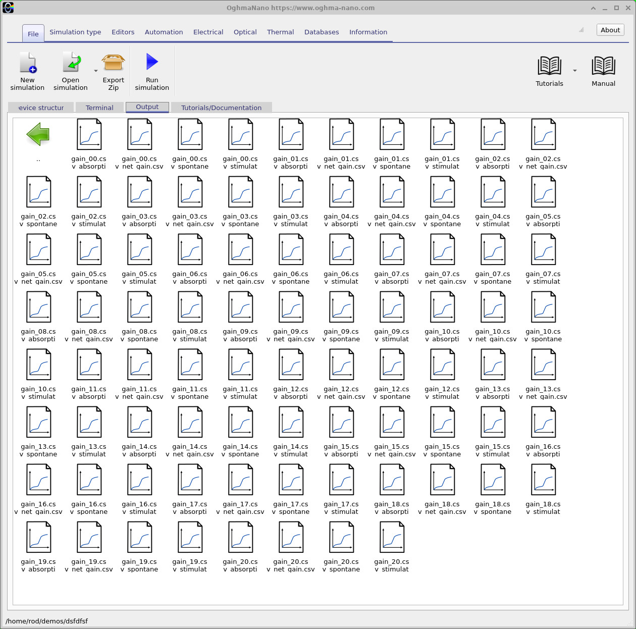
Open the Output tab in the main window after the simulation completes
(??).
The example writes separate CSV results for the various spectral calculations.
Visible filenames include entries following the patterns
gain_00.csv with absorption, net gain,
spontaneous and stimulated suffixes, followed by similarly named
files for subsequent calculated conditions. Double-click a result to inspect it in the
plotting window. Because the results are saved as CSV files, they can also be analysed
or replotted outside OghmaNano.
The numbered files let you follow how the calculated spectrum changes across the series of carrier conditions, rather than looking at only one optical calculation.
8. Try it yourself: change the well width
Suggested experiment: Return to the Layer editor and change the GaAs (QW) thickness from 10 nm to 8 nm, leaving the AlGaAs barrier layers unchanged. Rerun the simulation and compare the resulting subband energies and optical spectra against the original example.
- Does the lowest electron confinement level move upward relative to the GaAs conduction-band edge?
- How do the electron and hole transition energies change?
- Does the onset of the optical spectra shift towards shorter or longer wavelengths?
✅ Expected physical trend
A narrower well generally increases confinement energies. The lowest interband transition therefore tends to move to a higher photon energy, corresponding to a shorter wavelength, although the precise shift depends on the finite barrier heights and the electron and hole effective masses. Since \(\lambda=hc/E_{\mathrm{photon}}\), a higher transition energy means a smaller emission or absorption wavelength.
Once you are comfortable with this example, the natural next comparison is the 8-band zincblende k·p version of a GaAs/AlGaAs quantum well. It retains the quantum confinement but goes beyond independent parabolic bands to describe interactions and mixing between the conduction and valence states.
📘 For the detailed physics, continue with parabolic bands and the effective-mass approximation or the optical gain theory.