

What Is an Organic Field-Effect Transistor (OFET)?
1. What is an OFET?
An organic field-effect transistor (OFET) is a transistor in which an organic semiconductor forms the electrically active channel between a source and a drain electrode. Like a conventional field-effect transistor, the current through the device is controlled by a voltage applied to a third electrode called the gate. The gate is electrically isolated from the semiconductor by a dielectric layer, so it controls the channel mainly through its electric field rather than by injecting current directly into it.
The basic OFET structure therefore contains four important elements: a source, a drain, a gate dielectric and an organic semiconductor. The source and drain inject and collect charge carriers, while the gate changes the carrier density near the semiconductor–dielectric interface. By increasing or decreasing this interfacial charge density, the gate changes the conductivity of the channel and therefore controls the current flowing between source and drain.
OFETs are important because they provide transistor functionality using semiconducting materials that can be deposited from solution or by low-temperature thin-film processing. This makes them particularly useful for studying charge transport in organic semiconductors and for applications in areas such as flexible electronics, sensors, displays and organic integrated circuits.
2. Structure of an organic field-effect transistor
In the simplest picture, the organic semiconductor is separated from the gate electrode by an electrically insulating dielectric. The source and drain contacts are placed so that charge can move laterally through the semiconductor between them. Different OFET geometries place the contacts and gate above or below the semiconductor, but the same physical principle applies in each case: the gate electric field changes the carrier concentration close to the semiconductor–dielectric interface.
The region of increased carrier density close to this interface is usually called the accumulation channel. In a working transistor, most of the source–drain current flows through this relatively thin region rather than through the full thickness of the organic semiconductor. The properties of the semiconductor–dielectric interface can therefore strongly influence the electrical characteristics of the device.
The source and drain contacts also play an important role. Carriers must be injected from the metal contacts into the organic semiconductor before they can enter the channel. Differences between the contact work function and the semiconductor energy levels can create injection barriers and contact resistance, both of which can strongly influence the measured current.
3. How does a p-type OFET work?
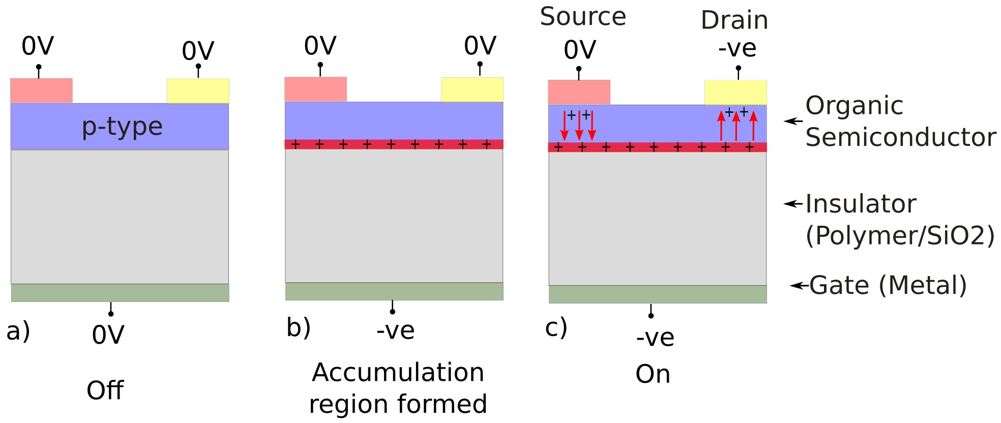
The most common introductory example is a p-type OFET, in which holes are the dominant mobile carriers. The operating sequence is illustrated in ??.
With the source, drain and gate close to the same potential, there is little gate-induced charge at the semiconductor–dielectric interface and the channel has a relatively low conductivity. Applying a negative gate voltage changes the electrostatic potential in the semiconductor and attracts holes towards the semiconductor–dielectric interface. As the hole density increases, an accumulation channel is formed.
Once this channel is present, applying a voltage between the source and drain produces a lateral electric field along the transistor. Holes then move through the accumulation layer, producing a source–drain current. Making the gate voltage more negative generally increases the hole density in the channel and therefore increases the channel conductivity.
The gate thus controls the source–drain current without needing to carry a significant steady-state current itself. Ideally, the gate dielectric blocks charge transport, so the gate behaves approximately like one electrode of a capacitor while the semiconductor channel responds electrostatically to the applied gate voltage.
4. n-type and ambipolar OFETs
OFETs can also operate as n-type devices. In an n-type OFET, electrons are the dominant carriers and a gate voltage of the opposite polarity is normally used to accumulate electrons at the semiconductor–dielectric interface. The resulting electron channel then carries current between source and drain.
Some organic semiconductors can transport both electrons and holes. Devices made from these materials are described as ambipolar OFETs. Depending on the applied gate and source–drain voltages, the device can operate in an electron-transport regime, a hole-transport regime, or under conditions where both carrier types contribute.
Whether an OFET behaves as p-type, n-type or ambipolar depends on the semiconductor energy levels, the source and drain contact properties, charge trapping, the dielectric interface and the surrounding environment. The observed device polarity is therefore a property of the complete transistor structure rather than of the semiconductor alone.
5. OFET transfer and output characteristics
OFET behaviour is commonly measured using two types of current–voltage characteristic. A transfer characteristic measures the drain current while the gate voltage is varied at a fixed source–drain voltage. This shows how effectively the gate switches the conducting channel on and off.
An output characteristic measures the drain current as the source–drain voltage is varied for one or more fixed gate voltages. At relatively small source–drain voltage the channel behaves approximately as a gate-controlled resistor and the current increases with source–drain bias. At larger bias, the carrier density becomes non-uniform along the channel and the device can enter a saturation-like regime in which the current becomes less sensitive to further increases in drain voltage.
Together, transfer and output characteristics provide information about charge transport, channel formation, threshold behaviour, contact effects and the overall electrical quality of the transistor.
6. Basic OFET equations
A useful first approximation is to treat the gate, dielectric and accumulated semiconductor charge as a capacitor. The capacitance per unit area of the gate dielectric is
\[ C_i = \frac{\varepsilon_0\varepsilon_r}{d} \]
where \(\varepsilon_0\) is the vacuum permittivity, \(\varepsilon_r\) is the relative permittivity of the gate dielectric and \(d\) is its thickness. In the simplest field-effect picture, the gate-induced sheet charge in the channel is approximately proportional to the gate overdrive,
\[ |Q| \approx C_i |V_G-V_T| \]
where \(V_G\) is the gate voltage and \(V_T\) is the threshold voltage. This relation explains why a thinner dielectric or a dielectric with a larger relative permittivity can produce more accumulated charge for a given gate voltage.
For an ideal long-channel transistor with approximately constant mobility, the magnitude of the drain current in the linear regime can be written as
\[ |I_D| = \mu C_i \frac{W}{L} \left[|V_G-V_T||V_D|-\frac{V_D^2}{2}\right] \]
where \(\mu\) is the field-effect mobility, \(W\) is the channel width, \(L\) is the channel length and \(V_D\) is the source–drain voltage magnitude. At sufficiently large drain bias, the ideal gradual-channel model gives a saturation current of
\[ |I_{D,sat}| = \frac{1}{2}\mu C_i\frac{W}{L}|V_G-V_T|^2. \]
These equations are useful for understanding and extracting approximate device parameters, but real OFETs can depart significantly from the ideal model because mobility may depend on carrier density and electric field, contacts may limit injection, and trapping can alter both the channel charge and the apparent threshold voltage.
7. What determines OFET performance?
Several physical quantities control the electrical behaviour of an OFET. One of the most important is the carrier mobility, which describes how readily charge carriers move through the organic semiconductor in response to an electric field. Higher mobility generally produces a larger source–drain current for the same device geometry and applied voltages.
The threshold voltage describes the gate-voltage scale over which a strongly conducting channel develops. In real organic devices it can be influenced by trapped charge, fixed charge in the dielectric, interface states and the energetic distribution of states in the semiconductor.
Contact resistance can also be important, particularly when injection from the source or extraction at the drain is inefficient. In this case a significant fraction of the applied source–drain voltage can be lost close to the contacts rather than across the transistor channel itself.
Charge trapping is especially important in many organic semiconductors. Traps can reduce the density of mobile carriers, shift the apparent threshold voltage, produce hysteresis and change the shape of the measured current–voltage characteristics. The gate dielectric and the semiconductor–dielectric interface can therefore be as important as the bulk mobility of the organic semiconductor.
8. OFETs compared with conventional MOSFETs
The operating principle of an OFET is closely related to that of a conventional MOSFET: in both devices, a gate electrode controls the carrier density in a semiconductor through an insulating dielectric. The main difference is the semiconductor material and the transport physics associated with it.
Conventional silicon MOSFETs use a crystalline inorganic semiconductor with well-defined conduction and valence bands and highly controlled doping. OFETs instead use organic semiconductors, where structural disorder, molecular packing, localized states, traps and contact injection can play a much larger role. As a result, the same basic field-effect concept is retained, but the microscopic description of charge transport can be substantially different.
👉 Key point: An OFET is a gate-controlled transistor in which an organic semiconductor carries current between source and drain. The gate does not normally supply the channel current directly; instead, its electric field creates or removes an accumulation layer at the semiconductor–dielectric interface.
9. Simulating an OFET
A numerical OFET model can be used to connect the applied terminal voltages to the internal electrostatic potential, carrier densities, current flow and charge accumulation within the device. This makes it possible to examine quantities that are difficult to measure directly, such as the spatial distribution of charge in the channel, the electric field near the contacts and the effect of traps or mobility on the current–voltage characteristics.
OghmaNano can simulate OFETs in two dimensions, including the source, drain, gate dielectric and organic semiconductor. The OFET tutorial shows how to create a p-type transistor structure, apply the terminal voltages and inspect the resulting source, gate and drain current–voltage curves.
👉 Continue to the OFET simulation tutorial to build and run a 2D organic field-effect transistor model in OghmaNano.
👉 Next step: For a broader introduction to organic semiconductor devices, see the introduction to organic electronics.