Organic semiconductor device simulation: OPVs, OLEDs and OFETs
1. Introduction to organic semiconductors
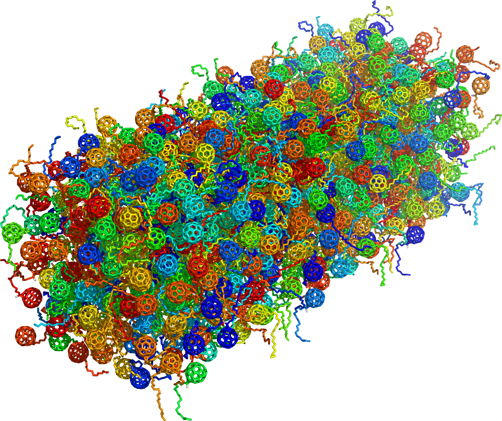
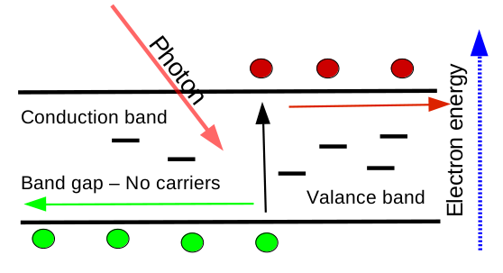
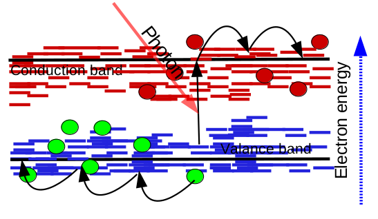
Organic semiconductors are carbon-based materials formed from polymers and small molecules rather than crystalline lattices. As a result, they resemble disordered molecular assemblies rather than periodic solids (see ??). This gives them attractive properties such as low-temperature processing and potentially low fabrication cost, but it also introduces significant structural and energetic disorder. Unlike silicon or III–V semiconductors, where carriers move in well-defined bands (see ??), charge transport in organic materials occurs through a broad distribution of localized states (see ??).
The consequence for device physics is that transport is not band-like but typically trap-limited and thermally activated. Carriers hop between localized states, are repeatedly captured and released by traps, and experience a spatially and energetically disordered landscape. The density of states is therefore not a sharp band edge but a distribution, and the occupation of that distribution evolves with bias, illumination and position within the device. The measured current–voltage response is thus a coupled signature of mobility, trap filling, recombination, internal electric field redistribution and contact injection.
For simulation, this means that trap states and disorder must be treated explicitly. Treating traps as a small perturbation is usually incorrect: in many organic devices, they are the dominant physics. Realistic models must therefore include both trap-state distributions and Shockley–Read–Hall (SRH) recombination, which together describe carrier capture, emission and recombination through localized states. These processes control carrier lifetimes, recombination pathways and ultimately device efficiency.
2. Why use OghmaNano for organic devices?
Organic semiconductor devices are governed by disorder, trapping and recombination, all of which are strongly coupled. Changes in bias or illumination alter trap occupation, which in turn modifies carrier density, recombination and the internal electric field. Below is an overview of tutorials and manual pages to help you get started with simulating organic electronic devices.
OghmaNano explicitly treats trap states using a dynamic Shockley–Read–Hall (SRH) model that accounts for both charge accumulation in trap states and carrier trapping and release through them. Without this, simulations will not accurately capture recombination or extract physically meaningful charge carrier mobility.
3. Organic device tutorials
These tutorials introduce the main organic device classes supported by OghmaNano. The OPV tutorial is the recommended starting point because it exposes the full device-modelling chain: optical absorption, charge generation, drift–diffusion transport, recombination and extraction. Once this workflow is understood, the same physical framework can be applied to OLEDs, OFETs and more specialised disordered semiconductor structures.
- Organic solar cell (OPV) simulation — build a complete organic photovoltaic simulation, calculate a JV curve, and interpret \(J_{SC}\), \(V_{OC}\), fill factor and efficiency in terms of generation, recombination, mobility, traps and contact extraction.
- Organic field-effect transistor (OFET) simulation — model organic transistor operation where electrostatics, gate-induced accumulation, contact injection, mobility and disorder-controlled transport determine the measured output.
- OLED device simulation - coherent thin-film optics — simulate OLED optical fields using coherent thin-film optics, where interference, layer thickness and refractive-index contrast control the optical environment inside the device.
- OLED device simulation - incoherent 3D optics — explore OLED light extraction and optical propagation using ray-tracing methods suited to thicker, textured or geometrically complex optical structures.
4. Organic solar cell device physics
Organic solar cells are controlled by the interaction between disorder, morphology and recombination. A high-quality OPV simulation must therefore go beyond fitting a JV curve. It must resolve how charge carriers are generated, how they move through a disordered density of states, how traps fill under bias, and how recombination changes with carrier density, electric field and spatial position.
- Space-Charge Limited Current (SCLC) example — study injection, space-charge formation and trap-limited current flow. SCLC simulations are important because the apparent mobility extracted from experiment often contains contributions from contacts, traps, energetic disorder and field redistribution.
- Large area OPV device simulation — move from idealised small-area cells to larger devices where sheet resistance, lateral current flow, contacts and scaling losses become part of the device physics.
- Simulating bulk-heterojunction morphologies with 2D electrical slices — examine how nanoscale phase separation, percolation pathways and donor-acceptor geometry influence extraction, recombination and local carrier accumulation in BHJ solar cells.
5. Excited states and exciton physics
In organic optoelectronic devices, optical absorption usually creates bound excitons rather than immediately producing free carriers. This is one of the central differences between organic and conventional inorganic semiconductor device modelling. The simulation must therefore include not only where photons are absorbed, but also where excitons diffuse, where they dissociate, and where they are lost before producing useful charge.
This matters especially in bulk heterojunctions, where the relevant length scales are often comparable to exciton diffusion lengths. Morphology is therefore not a decorative structural detail: it determines whether absorbed light becomes extracted charge, geminate loss, non-geminate recombination or heat.
- Exciton dynamics in OPV devices — simulate exciton generation, diffusion, dissociation and loss in organic photovoltaic devices, and connect optical absorption to free-carrier generation.
- Exciton transport in BHJ domains — examine exciton motion in spatially structured donor-acceptor domains where domain size, interface area and diffusion length control charge generation.
6. Frequency-domain simulations: IS, IMPS and IMVS
Frequency-domain measurements are powerful because they probe the internal time constants of a device rather than only its steady-state output. In disordered organic semiconductors, those time constants are rarely simple. They can arise from transport delay, trapping and release, chemical capacitance, contact effects, recombination kinetics, ionic motion or morphology-dependent extraction.
OghmaNano’s frequency-domain simulations allow these effects to be studied from the same physical model used for the steady-state device. This is important: IS, IMPS and IMVS are most useful when they are not treated as separate equivalent-circuit fitting exercises, but as dynamic probes of the same drift–diffusion, trap and recombination physics that controls the JV curve.
- Impedance spectroscopy (IS) — analyse small-signal electrical response, capacitance, transport resistance and frequency-dependent recombination in simulated organic devices.
- Intensity-Modulated Photocurrent Spectroscopy (IMPS) — study photocurrent response under modulated illumination, linking extraction dynamics to carrier transport and recombination.
- Intensity-Modulated Voltage Spectroscopy (IMVS) — study voltage response under modulated illumination, often used to probe recombination lifetimes, charge storage and quasi-Fermi-level dynamics.
7. Organic thermal modelling
Temperature is not a secondary parameter in disordered organic semiconductors. Because hopping, trapping, release, recombination and mobility are often thermally activated, even modest self-heating can change the apparent transport and recombination behaviour of a device. In high current-density devices, large-area modules and poorly heat-sunk structures, electro-thermal coupling can therefore affect both performance and interpretation.
- Electro-thermal simulation: self-heating tutorial — model heat generation, thermal transport and temperature-dependent device behaviour in organic semiconductor structures.
8. Underlying physics
The tutorials above are built on OghmaNano’s drift–diffusion and optical modelling framework. For disordered semiconductors, the critical point is that carrier density, mobility and recombination are not independent knobs. They are coupled through the density of states, trap occupation and internal electrostatic potential. A change in illumination, bias or contact boundary condition changes trap filling; trap filling changes the free-carrier population; the free-carrier population changes recombination and conductivity; and the resulting field redistribution changes extraction.
This is why OghmaNano places trap-state physics, SRH recombination, non-equilibrium trapping, optical generation and drift–diffusion transport in the same modelling environment. For organic semiconductors, separating these effects too aggressively often produces simulations that are easy to fit but physically misleading.
- Theory of drift–diffusion modelling — the electrical transport framework used to solve carrier continuity, current flow and electrostatic coupling in device simulations.
- The need for trap states in organic device models — why distributed trap states and energetic disorder are essential for modelling organic and other disordered semiconductors.
- Shockley–Read–Hall recombination — analytical treatment of trap-assisted recombination and the physical basis of trap-mediated carrier loss.
- Non-equilibrium SRH trapping and recombination — numerical treatment of trapping, emission and recombination in energy-resolved trap distributions, where equilibrium assumptions are not sufficient.
- Charge carrier mobility — mobility models, transport assumptions and the interpretation of mobility in disordered semiconductor devices.
9. Where should you start?
If you are new to OghmaNano, start with the OPV tutorial. It gives the fastest route to a complete organic semiconductor device simulation: define the stack, run the model, inspect the JV curve and connect the result to physical quantities such as generation, extraction, recombination and voltage loss.
If you already understand the basic workflow, move directly into the physics tutorials. Use SCLC to understand injection and trap-limited transport, the exciton tutorials to understand the conversion of absorbed light into free carriers, the BHJ tutorials to study morphology, and IS/IMPS/IMVS to connect the same physical model to dynamic experimental characterisation.