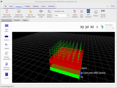
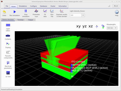
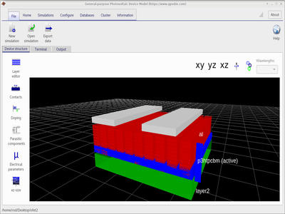
A particular strength of OghmaNano is the modelling of novel and disordered semiconductors.
Rather than assuming that all carriers remain in equilibrium, it can explicitly model trapping,
de-trapping and recombination using non-equilibrium Shockley–Read–Hall physics.
The same physical models can be explored under steady-state, transient and frequency-domain conditions,
allowing electrical, optical and spectroscopic measurements to be simulated within the same framework.
Advanced electrical transport:1D, 2D and 3D drift–diffusion simulation,
Poisson and carrier-continuity equations, Fermi–Dirac and Maxwell–Boltzmann statistics,
non-equilibrium SRH trapping and recombination,
Auger recombination,
interface transport, field-dependent mobility and energetic disorder.
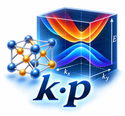
Quantum wells & electronic band structure:k·p band-structure modelling,
parabolic effective-mass quantum wells,
8-band and 10-band zincblende models,
8-band wurtzite models,
silicon Δ-valley calculations,
Luttinger–Kohn valence-band modelling,
and bulk perovskite band structures.
These models can be used to calculate confined states, band mixing,
optical transitions, gain, scattering and carrier mobility.
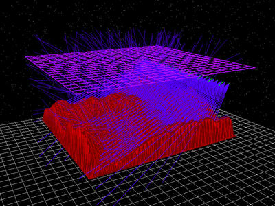
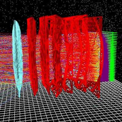
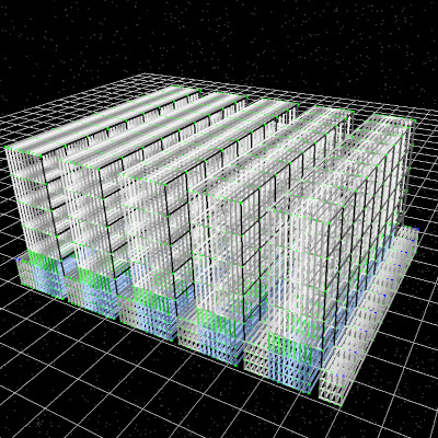
Wave optics & photonic devices:2D and 3D FDTD simulations
of resonators, waveguides, diffraction structures and integrated photonic systems,
together with
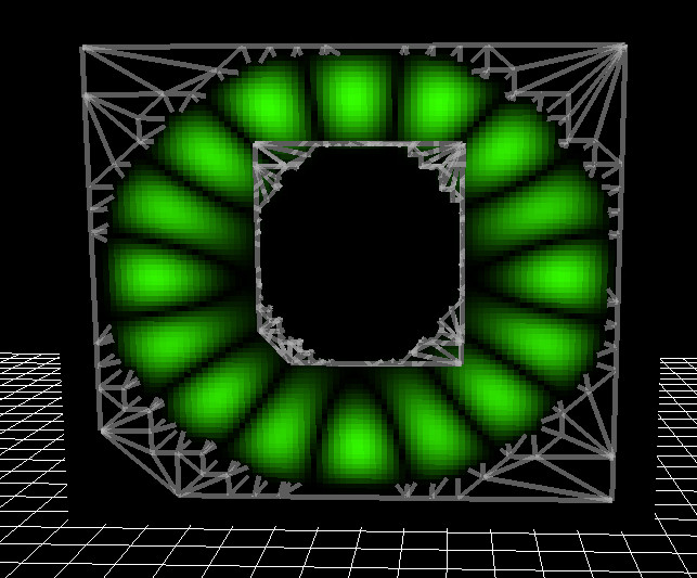
TE/TM optical mode solving
for waveguides and resonators.
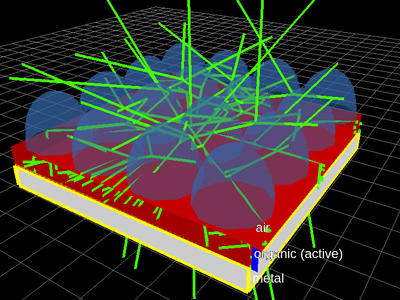
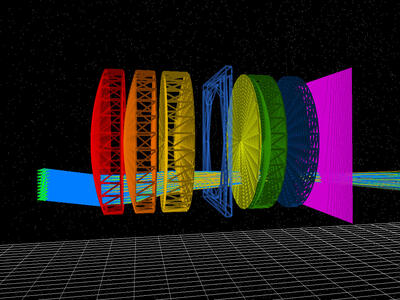
Ray tracing & optical systems:
geometrical-optics simulation of lenses and complex optical systems,
including
microlenses,
prime lenses,
Cooke triplets
and CAD-based optical geometries.
Carrier scattering & mobility:
acoustic-phonon scattering,
Fröhlich polar-optical-phonon scattering,
momentum-relaxation calculations,
carrier statistics and mobility derived directly from calculated band structures.
Optical and electrical observables:
photoluminescence and electroluminescence,
EQE,
Suns-Voc,
Suns-Jsc,
charge extraction, carrier density, recombination and energy-resolved trap occupation.
Parameter extraction & experimental fitting:automatic parameter fitting
of simulated data to experimental measurements across electrical, optical and spectroscopic datasets.
Thermal & coupled multiphysics modelling:
temperature-dependent material properties, heat generation and thermal transport,
with electrical, optical and thermal models combined within the same device simulation.
Material parameters such as mobility, energetic disorder, doping, and recombination can be modified directly through the
graphical interface, making it easy to explore how device physics influences performance.
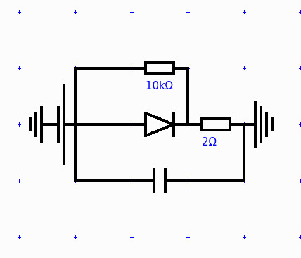
These capabilities are implemented through a set of complementary numerical solvers covering semiconductor transport, wave optics, geometric optics, and circuit modelling.
OghmaNano therefore combines semiconductor device modelling with modern photonics simulation tools, enabling both electrical and optical analysis within a single multiphysics environment.
OghmaNano numerically solves the fully coupled semiconductor device equations in steady-state or full time-domain form, in 1D, 2D, or full 3D.
The solver handles both electron and hole drift–diffusion and carrier continuity equations in real space, coupled self-consistently with Poisson’s equation to determine the internal electrostatic potential.
Recombination and carrier trapping are treated using a highly flexible Shockley–Read–Hall (SRH) formalism, with arbitrary user-defined trap distributions.
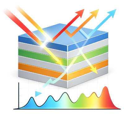
Optical generation profiles can be computed internally using the built-in transfer matrix and ray-tracing engines, or imported from external solvers such as FDTD packages.
The model supports steady illumination, voltage sweeps, arbitrary transient signals, and large-area / patterned-contact device simulations.
A more detailed description can be found in the manual, the associated publications, and the user documentation.

 ☰
☰
 Chinese (China),
 Ukrainian (Ukraine),
 Turkish,
 Russian (Russia),
 Portuguese (Portugal),
 Portuguese (Brazil),
 Polish (Poland),
 Malay,
 Latin,
 Georgian,
 Japanese,
 Italian (Italy),
 Hindi,
 Hebrew,
 French (France),
 Estonian (Estonia),
 Spanish (Spain),
 Greek (Greece),
 German (Germany),
 Welsh,
 Arabic,