Perovskite Solar Cell (PSC) Tutorial Part B: perovskite devices and light
To understand how perovskite devices absorb light, we first need to explore the optical data available inside OghmaNano. The software includes a built-in library of measured and standard spectra that you can use as illumination sources for your simulations.
1. Browsing OghmaNano’s optical databases
- Go to the Databases ribbon, as shown in ??.
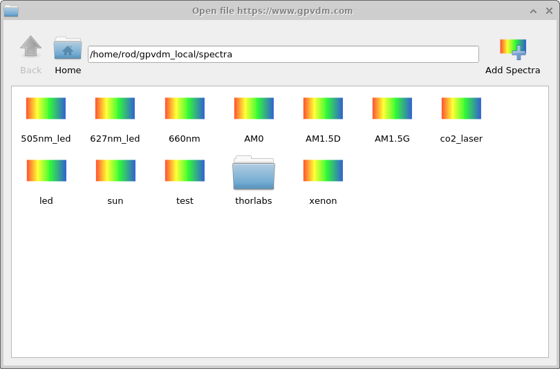
- Click the Optical database icon (rainbow). This opens the window shown in ??.
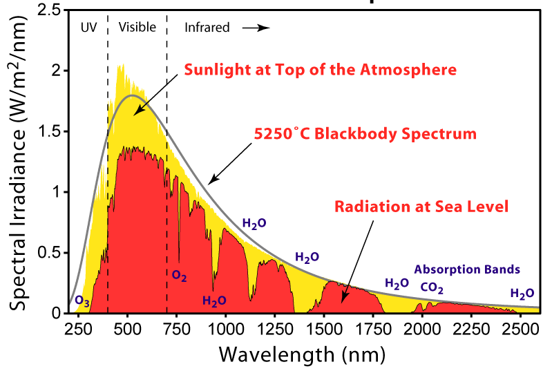
- Double-click AM1.5G to load the standard terrestrial solar spectrum. Note the region of maximum irradiance and the absorption “dips” caused by molecules in Earth’s atmosphere. The curve should look similar to ??.
2. Understanding the solar spectrum
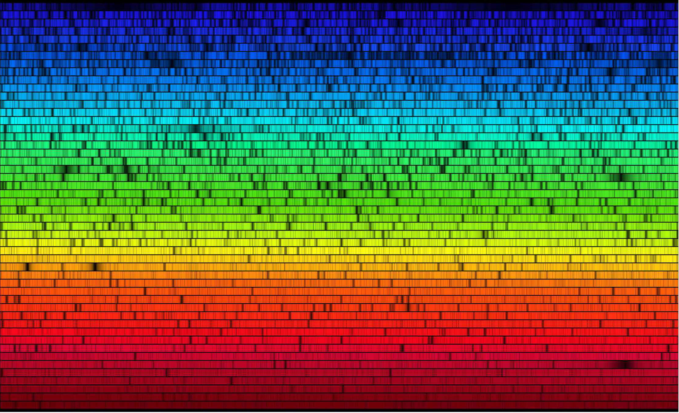
The performance of any solar cell depends strongly on the distribution of sunlight it receives. Because the Sun’s intensity changes with both time of day and geographical location, researchers use a reference spectrum called AM1.5G to make results comparable. Figures ?? and ?? illustrate this spectrum: a line plot of spectral irradiance versus wavelength and a false-colour representation across the visible band. AM1.5G corresponds to sunlight that has travelled through 1.5 times the Earth’s atmosphere compared to the Sun directly overhead, which approximates mid-latitude afternoon conditions. The dips in intensity are signatures of atmospheric absorption — ozone removes part of the UV, while water vapour and carbon dioxide absorb in the infrared. By using AM1.5G in simulation, your calculated device efficiencies can be compared on equal footing with published values, including the record efficiencies often quoted for perovskite solar cells.
3. How perovskite materials absorb light
A solar cell is built from several layers, each with its own function. Some transport charges, while others are
responsible for absorbing incoming photons. To examine the absorption spectrum of a perovskite material in OghmaNano,
open the Materials database from the
?? toolbar.
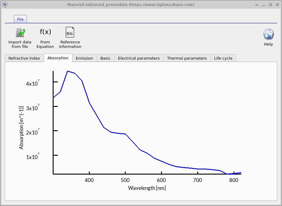
Navigate to the perovskite directory and select std_perovskite.
Under the Absorption tab
(??) you will see how strongly this material
absorbs light across the spectrum. This wavelength-dependent absorption is what defines how efficiently a perovskite
active layer can harvest sunlight.
perovskite directory and select std_perovskite.
The Sun provides a continuous range of wavelengths, but each region interacts differently with a perovskite solar cell:
- UV (≈200–400 nm): Much of this is filtered by the atmosphere and glass layers before reaching the device.
- Visible (≈400–700 nm): The primary absorption window for perovskites, where most of the power is harvested.
- Near-IR (≈700–2500 nm): Although this range carries significant solar energy, thin perovskite layers absorb it weakly, so much of it passes through or is reflected.
- Mid/Far-IR (>≈2500 nm): This is essentially heat radiation and is not useful for photovoltaic conversion.
3. Simulating light absorption
Having introduced the AM1.5G spectrum and the absorption properties of perovskite materials, we can now combine these ideas to simulate how photons are distributed and absorbed inside the full device stack. This step links the optical input from the Sun to the spatial profile of charge generation within the cell.
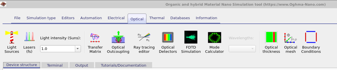
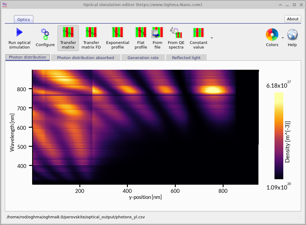
Open the Optical ribbon (Figure ??) and choose Transfer Matrix Simulation. In the window that appears, click Run optical simulation (blue play button). OghmaNano will calculate wavelength- and position-resolved optical fields using the transfer-matrix method.
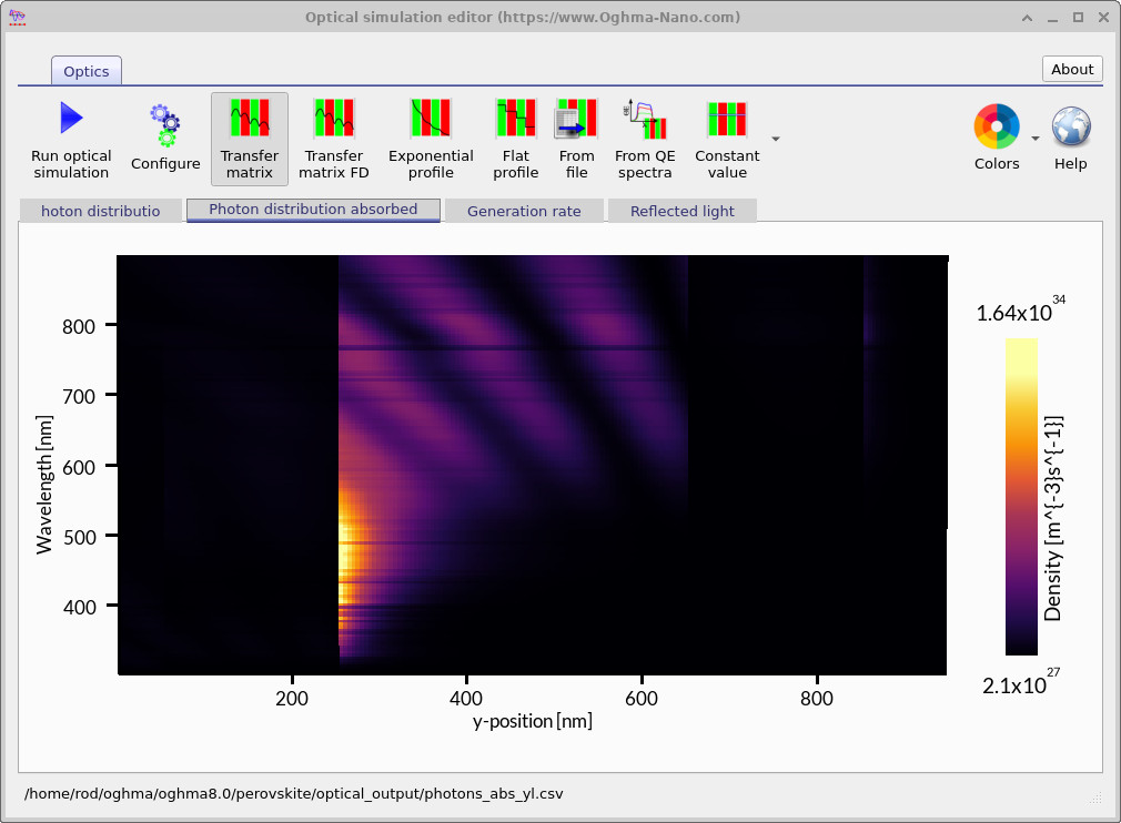
The simulation produces several visualisations. The first is the Photon density map, which shows how the optical field is distributed throughout the device as a function of both wavelength and position (Figure ??). Bright regions correspond to standing-wave patterns and high photon densities inside the perovskite layer and adjacent interfaces.
The second is the Photon absorption map, which directly indicates where photons are absorbed to create electron–hole pairs (Figure ??). This plot highlights which layers are responsible for harvesting sunlight and reveals how efficiently the perovskite layer captures incoming radiation across the solar spectrum.
📝 Questions (Part B)
- Which reference solar spectrum is typically used when simulating perovskite devices?
- The AM1.5G spectrum shows many small “dips”. What causes these features?
- Across which region of the spectrum (UV, visible, IR) do perovskite active layers absorb most strongly?
- Looking at the absorption maps, why does the transparent ITO layer show almost no absorption?
- What insight does the 1D absorption (generation) profile give about where carriers are created in the device?