Perovskite Solar Cell (PSC) Tutorial - Part F: Contacts
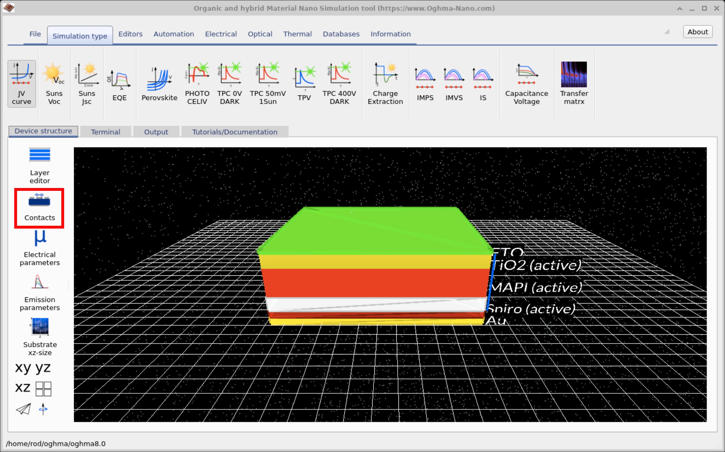
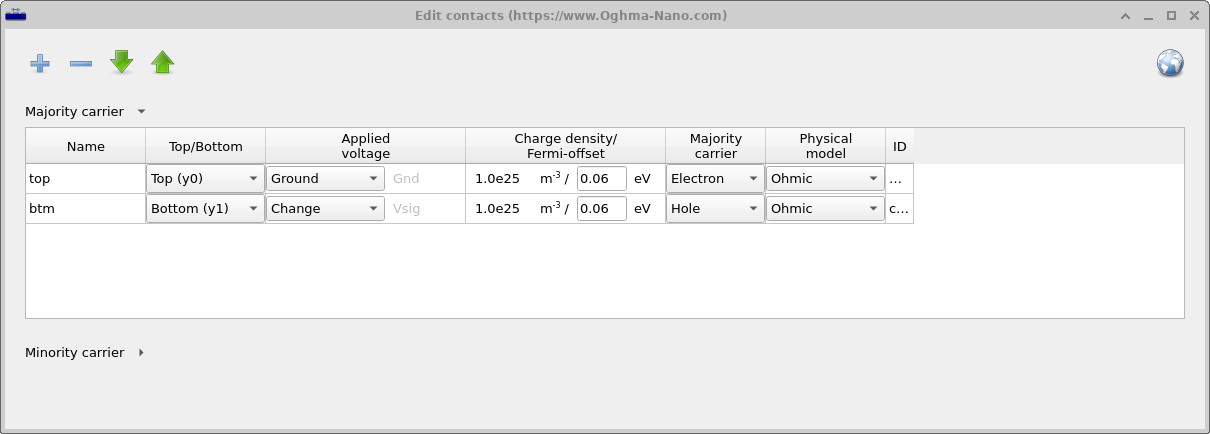
Perovskite solar cells require electrical contacts for biasing and current collection. In OghmaNano, contacts are set in the Contact editor, opened via the Contacts button (see ??). The editor window (??) lets you define contact position and electrical properties such as bias type, majority carrier, and boundary condition.
Columns in the Contact editor
- Name — A label (e.g. “Au anode”, “TiO₂ cathode”); used for clarity only.
- Top/Bottom — Contact placement in the stack. In n–i–p devices the bottom is the electron-selective cathode (FTO/TiO₂) and the top the hole-selective anode (Spiro-OMeTAD/Au). In 2D geometries, left/right orientations are also supported.
- Applied voltage — Biasing mode:
- Ground: Fixed at 0 V (reference).
- Constant bias: Fixed at a chosen voltage.
- Change: Swept or perturbed terminal (used in JV, impedance, transients).
- Charge density / Fermi offset — Defines majority carrier density at the interface. High values yield ohmic, selective contacts; low values mimic blocking contacts that often cause S-shaped JV curves.
- Majority carrier — Selects whether the contact conducts electrons or holes. In MAPbI₃ n–i–p devices: bottom/TiO₂ extracts electrons, top/Spiro–Au extracts holes. Inverted p–i–n devices reverse these roles.
- Physical model — Contact boundary condition:
- Ohmic: Efficient majority carrier extraction/injection (default).
- Schottky: Barrier-limited transport, useful for studying blocking and VOC losses.
Tip: For JV sweeps, mark one terminal as Change and keep the other at 0 V. To study perovskite contact losses, try lowering the majority carrier density or switching to a Schottky model. This often produces S-shaped JV curves and lower VOC, revealing the role of imperfect contacts.
Show suggested answer
Reducing majority carrier density weakens contact selectivity and increases resistance. The result is poorer extraction and a shift away from ideal ohmic behaviour:
- VOC: Often drops due to enhanced recombination at the interface.
- FF: Declines noticeably, producing an S-shape or roll-off in the JV curve.
- JSC: Initially stable, but can fall if extraction becomes strongly limited.
- PCE: Decreases mainly through FF and VOC losses.
Physically, this mimics moving from a well-aligned, selective contact to a resistive one — a common failure mode in perovskite solar cells.
📝 Check your understanding (Part F – Contacts)
- In the Contact editor, which fields set (a) the driven terminal for a JV sweep and (b) the reference terminal?
- Explain the difference between Ground, Constant bias, and Change. When would you use each?
- What does the Majority carrier setting do, and how should it be configured for a non-inverted MAPbI₃ device?
- Describe the practical difference between the Ohmic and Schottky contact models. How might each influence VOC?
- How can reducing the majority charge density at an ohmic contact affect the JV curve (JSC, VOC, FF)? What physical effect is this mimicking?
- If only one contact is set to Change for a JV sweep, what should the other contact be set to, and why?
- Which contact collects electrons and which collects holes in a standard (non-inverted) MAPbI₃ cell, and how does misconfiguring this show up in the JV?
👉 Next steps:
- Return to the perovskite solar cell simulation guide for the full tutorial overview.